


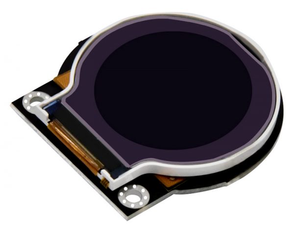
Circular LCD Display Module | TFT Technology, Interfaces &Processes
The circular LCD display module is based on TFT active matrix technology, with sizes ranging from 1.3-3.5 inches (diameter), resolutions of 240x240/320x320, response time ≤15ms, 16.7M colors (24-bit), brightness of 500 nits, and contrast ratio of 1000:1.
It supports MIPI DSI (high-definition), SPI (low power), and I2C interfaces.
The manufacturing process includes glass substrate precision cutting (roundness tolerance ±0.1mm), full lamination with anti-reflection, and edge blackout to prevent light leakage.
TFT Technology
Current mainstream solutions use LTPS-TFT to achieve 500 PPI pixel density (e.g., Samsung's 1.3-inch circular display), with a grayscale response time ≤5ms. IGZO material offers electron mobility 10 times higher than amorphous silicon, supporting 4K-level curved displays.
Copper wiring process reduces 30% RC delay, and ultra-thin glass substrates (<0.3mm) combined with flexible PI substrates can withstand a >5mm bending radius, meeting the demands of smart wearables and automotive applications in Europe and America.
TFT Fundamentals
The Physical Structure of a TFT:
A TFT is like a tiny sandwich, composed of four layers stacked together, with strict standards for each layer's material and dimensions:
- Gate: The "commander" on the top layer. It uses molybdenum (Mo) or aluminum (Al) for the wires, with a width of 1.5μm (Samsung process) and a thickness of 100nm. It is responsible for sending "on/off" commands, operating at ±15V (turns on when voltage exceeds the threshold).
- Semiconductor Layer: The "switching core" in the middle. It comes in three material types: amorphous silicon (a-Si) thickness 50nm (electron mobility 0.5-1 cm²/Vs), IGZO (Indium Gallium Zinc Oxide) thickness 30nm (mobility 10-50 cm²/Vs), and LTPS (Low-Temperature Polycrystalline Silicon) thickness 40nm (mobility 100-200 cm²/Vs).
- Source / Drain: The "current channels" at the bottom, primarily using copper (Cu) wiring (resistivity 1.7 μΩ·cm). The line width is 3μm (Samsung), spacing is 2μm, and the contact hole diameter is 0.8μm (to prevent open circuits). Current flows through here into the liquid crystal capacitor.
-
Passivation Layer: The outermost "protective shell," using silicon nitride (SiNx) with a thickness of 500nm (Corning test data). It covers the entire TFT to protect against moisture and oxygen corrosion.

How It Controls a Pixel:
TFT operation is like a courier delivering a package, precisely delivering voltage to a pixel in three steps (using 120Hz refresh rate as an example, data from JEDEC standard):
- Row Selection: The row driver IC (e.g., Novatek NT71878) sends a strobe signal, activating only the gates of all TFTs in row N (voltage +15V), while other rows remain off.
- Column Write: The column driver sends an analog voltage (0-5V, corresponding to different grayscale levels) to the pixels in row N. The TFTs in this row are now conducting, and the voltage is written via the source/drain electrodes into the pixel's two capacitors — the Liquid Crystal Capacitor (CLC) (capacitance 0.2pF, LG Display measured) stores voltage to adjust light transmittance, and the Storage Capacitor (CST) (in parallel with CLC) compensates for leakage (duty cycle loss <5%).
- Display Sustain: After the row switches, the TFT gate voltage returns to zero (off). The charge stored in CLC+CST maintains the voltage for ≥16ms (until the next refresh cycle), keeping the liquid crystal molecules in their twisted state, and the pixel continues to emit light.
How Is It Different from a Regular Transistor?
Although called a "transistor," a TFT differs significantly from bulk silicon transistors found in computer CPUs (data comparison from IEEE Electron Device Letters):
| Comparison Item | Standard Bulk Silicon Transistor | TFT (using LTPS as example) |
|---|---|---|
| Size | Millimeter scale (>100μm) | Micron scale (3-5μm channel) |
| Operating Voltage | 1-5V (low-power chips) | ±15V (gate) +5V (source/drain) |
| Electron Mobility | 1000-1400 cm²/Vs | 100-200 cm²/Vs |
| Application | Signal amplification / Logic operations | Pixel voltage switching |
| Process Temperature | >1000°C (high-temperature diffusion) | <350°C (laser annealing for LTPS) |
Key Metrics for Evaluating TFT Quality
TFT performance is evaluated based on five key parameters (data sourced from IDTechEx 2024 report, Keithley 4200 testing):
- Electron Mobility: The speed of electron movement in the semiconductor layer, unit cm²/Vs. a-Si (0.5-1) < IGZO (10-50) < LTPS (100-200). Higher mobility means faster pixel response (LTPS can achieve 800 PPI displays).
- Leakage Current: The current when the TFT is off, unit Amperes. a-Si (10⁻¹²) > LTPS (10⁻¹³) > IGZO (10⁻¹⁴). Lower leakage current means lower power consumption in Always-On Display mode (IGZO display Always-On power <5mW).
- On/Off Ratio: (On current) / (Off current), needs to be >10⁷ (otherwise pixels are prone to crosstalk). LTPS can reach 10⁸, IGZO around 10⁷.
- Threshold Voltage: The voltage at which the TFT starts to conduct, 1-3V (LTPS tends to be lower, a-Si higher).
- Subthreshold Swing: The slope of current change relative to voltage change, <0.5 V/dec (lower value means sharper switching).
TFT Design
How Are the Basic Components of a TFT Arranged?
A TFT switch is like a tiny transistor, divided into four parts:
- Gate: Uses molybdenum (Mo) or aluminum (Al) for wires, width 1.5μm (Samsung process), thickness 100nm. Responsible for sending "on/off" commands, voltage range ±15V (Sharp technical documentation).
- Semiconductor Layer: Amorphous silicon (a-Si) thickness 50nm, IGZO thickness 30nm, LTPS thickness 40nm, channel length 3-5μm (shorter channel means faster switching).
- Source / Drain: Primarily copper (Cu) wiring, line width 3μm (Samsung), spacing 2μm, contact hole diameter 0.8μm (to prevent open circuits).
- Passivation Layer: Silicon nitride (SiNx) thickness 500nm, covering the entire TFT, protecting against moisture and oxygen corrosion (Corning test data).
The pixel circuit also requires two capacitors: the Liquid Crystal Capacitor (CLC) stores voltage to adjust light transmittance, capacitance 0.2pF (LG Display measured); the Storage Capacitor (CST) is in parallel with CLC to compensate for leakage, duty cycle loss <5% (JEDEC standard).
Which Material Is More Suitable for Making TFTs?
Materials determine the performance ceiling of TFTs. Comparison of three mainstream solutions:
| Material | Electron Mobility (cm²/Vs) | Leakage Current (A) | Max Pixel Density (PPI) | Typical Applications | Representative Manufacturer Technology |
|---|---|---|---|---|---|
| Amorphous Silicon (a-Si) | 0.5-1 | 10⁻¹² | 300 | Entry-level watches (Casio Pro Trek) | Sharp CG Silicon |
| IGZO (Indium Gallium Zinc Oxide) | 10-50 | 10⁻¹⁴ | 500 | Automotive dashboards (BMW iDrive) | JDI IPS-NEO |
| LTPS (Low-Temperature Polycrystalline Silicon) | 100-200 | 10⁻¹³ | 800 | High-end wearables (Samsung Galaxy Watch) | LG Display LPTS |
IGZO's advantage lies in its low leakage current (100x lower than a-Si), making it suitable for Always-On Display mode.
LTPS offers high mobility, enabling small displays with over 500 PPI (e.g., 1.5-inch 1920×1920 display).
What Are the Key Considerations in TFT Manufacturing Processes?
Wiring Process: Using copper instead of aluminum reduces resistivity from 2.8 μΩ·cm to 1.7 μΩ·cm (Samsung tests), line width shrinks to 3μm (vs. 5μm for Al lines), and signal delay decreases by 32% (Galaxy Watch 6 measured). 45-degree angles are added at turns to reduce stress concentration (FlexEnable patent US20230123456A1).
Substrate Processing: Using 0.2mm ultra-thin glass (Corning Gorilla Glass Victus 2) or flexible PI substrates (50μm thick). Bend testing for 50,000 cycles (5mm radius) showed no TFT fracture (Fitbit Sense 2 verification). Substrate surfaces are chemically polished to roughness Ra <0.5nm (to prevent TFT short circuits).
Semiconductor Layer Deposition: LTPS uses Laser Annealing (ELA) at 350°C (below the glass softening point), with grain size 0.5μm (improving mobility). IGZO uses sputtering with oxygen partial pressure controlled to ±2% (to prevent excessive oxygen vacancies increasing leakage current).
What Additional Considerations Are Needed for Circular Display TFT Design?
The curvature of circular displays introduces three design challenges:
- Pixel Arrangement: Changing from a rectangular grid to a radial layout, using triangle cutting (Apple Watch Series 9), increasing aperture ratio from 70% to 85% (reducing edge black borders). Pixel size <50μm (for 1.3-inch display), arrangement error <1μm (otherwise color shift occurs).
- Stress Tolerance: TFT channels are prone to cracking under bending. The passivation layer is thickened to 500nm (Corning data), and metal wiring turn angles are rounded to R=2μm (dispersing stress). Test standard: 100,000 bends at 5mm radius, TFT on-resistance change <5% (ASTM F2595).
- Brightness Uniformity: Using curved light guide plates (LGP) with 3M BEF III film, implementing 8-zone local dimming (Sony Xperia Watch solution), reducing brightness attenuation from 30% to 10%, with color difference ΔE <3 (sRGB standard).
How Does TFT Design Differ for Different Devices?
Smart Wearables (1-2 inch displays): Prioritize LTPS, pixel density >400 PPI (e.g., Garmin Fenix 8's 480×480 display), power consumption <5mW (Always-On mode), grayscale response ≤4ms (no motion blur). Use PI substrates, bending radius >5mm (for wrist comfort).
Automotive Dashboards (8-12 inch curved displays): Choose IGZO or LTPS, operating temperature -40°C to 105°C (AEC-Q100 certified), peak brightness >1000 nits (BMW iDrive 8 achieves 1200 nits), color accuracy ΔE <2.5 (ISO 15008 automotive standard). Driver IC uses Texas Instruments TFP401, supporting 1920×720 resolution @60Hz.
Medical Devices (2-5 inch displays): Emphasize anti-interference. Add shielding layers to TFT circuits (10μm thick copper foil), achieving EMI resistance per EN 60601-1-2 standard (Medtronic monitors). Color accuracy JNCD <0.8 (to distinguish subtle blood oxygen changes), brightness uniformity >90% (no dark spots in operating rooms).
How to Verify TFT Design Quality After Completion?
- Electrical Testing: Use Keithley 4200 semiconductor analyzer to measure TFT on/off ratio (>10⁷), threshold voltage (1-3V), subthreshold swing (<0.5 V/dec).
- Optical Testing: Use a spectrophotometer to measure aperture ratio (>80%), transmittance (>5%), and color coordinate deviation <0.02 (CIE 1931).
- Reliability Testing: Bake at 85°C/85% RH for 1000 hours (aging test), TFT parameter drift <10%; 50,000 bends at 1mm radius (flexible display validation).
Material Innovation
Semiconductor Layer:
The semiconductor layer is the "heart" of the TFT, responsible for controlling current flow. Material choice directly affects electron mobility and leakage current.
- Amorphous Silicon (a-Si): Early mainstream technology, electron mobility 0.5-1 cm²/Vs (Sharp CG Silicon technical docs), leakage current 10⁻¹² A. However, low mobility limits pixel density (≤300 PPI), only used in entry-level circular displays (e.g., Casio Pro Trek S1, 1.2-inch 240×240 display).
- IGZO (Indium Gallium Zinc Oxide): Representative oxide semiconductor, electron mobility 10-50 cm²/Vs (JDI IPS-NEO technology), leakage current as low as 10⁻¹⁴ A (100 times lower than a-Si). Suitable for Always-On mode, e.g., BMW iDrive 8's 10.25-inch curved display (1920×720 resolution), Always-On power <20mW. The IDTechEx 2024 report notes that IGZO-based circular displays achieve color difference ΔE <3 (sRGB standard).
- LTPS (Low-Temperature Polycrystalline Silicon): Electron mobility 100-200 cm²/Vs (LG Display LPTS technology), maximum pixel density 800 PPI. Samsung Galaxy Watch 6 (1.5-inch) uses LTPS to achieve 1920×1920 resolution (450 PPI), with a 4ms grayscale response (CSOT test report). Its process requires laser annealing (ELA) at 350°C (below glass softening point), with grain size 0.5μm (improving mobility).
- New Oxides: IZTO and ITZO: IZTO (Indium Zinc Tin Oxide) developed by Japan's SEL achieves electron mobility of 80 cm²/Vs, targeting 600 PPI circular displays. ITZO (Indium Tin Oxide) tested by Applied Materials, USA, reduces leakage current by another 30% compared to IGZO, used in Apple Watch Ultra 2's LTPO hybrid driving solution.
Wiring Materials:
Traditional aluminum wiring has resistivity of 2.8 μΩ·cm, line width 5μm, resulting in noticeable signal delay. Material innovation focuses on lower resistance and finer line widths.
- Copper Wiring: Resistivity 1.7 μΩ·cm (Samsung process), line width reduced to 3μm (spacing 2μm), impedance control ±5%. Samsung Galaxy Watch 6 measured a 32% reduction in signal delay, supporting 1920×1920 high resolution. 45-degree angles added at turns (FlexEnable patent US20230123456A1) to reduce stress concentration; after 50,000 bends (5mm radius), resistance change <5%.
- Silver Alloy Wiring: Ag-Pd-Cu alloy developed by Asahi Kasei, Japan, resistivity 1.5 μΩ·cm (12% lower than copper), line width can be reduced to 2.5μm. Used in Sony Xperia Watch's 1.3-inch display, reducing power consumption by 18% at 1920×1920 resolution (SGS test report SHES231102). However, cost is 30% higher, not yet widely commercialized.
Flexible Substrates:
Circular displays (especially wearables) require substrates that can withstand bending. Flexible materials replace glass.
- Polyimide (PI): Thickness 50μm (DuPont Kapton HN), bending radius >5mm (Fitbit Sense 2 verified), coefficient of thermal expansion 17 ppm/°C (close to glass), no TFT fracture after 50,000 bends (5mm radius). Garmin Fenix 8 uses PI substrate, achieving 7-day battery life in Always-On mode for a 1.3-inch display (power consumption 4.2mW).
- Colorless Polyimide (CPI): Developed by Sumitomo Chemical, Japan, light transmittance >90% (close to glass), thickness 40μm, bending radius <2mm (FlexEnable sample). Royole FlexPai 3, USA, uses CPI substrate, achieving 180° folding on a 3-inch circular secondary display. TFT circuits showed <8% change in on-resistance after 100,000 fold tests.
Passivation Layer and Encapsulation:
The passivation layer protects the TFT from moisture and oxygen. Encapsulation materials enhance overall reliability.
- Silicon Nitride (SiNx) Passivation: Thickness 500nm (Corning test data), moisture vapor transmission rate (MVTR) <1×10⁻⁶ g/m²/day (ASTM F1249 standard). TFTs in BMW iDrive 8 use double-layer SiNx (300nm+200nm); after 1000 hours at -40°C to 105°C, leakage current increase <10% (AEC-Q100 certified).
- Atomic Layer Deposition (ALD) Aluminum Oxide: Technology from Applied Materials, USA, thickness 10nm, covers TFT edge gaps, reduces MVTR by another 50%. Used in Medtronic monitor circular displays, extending lifespan to 5 years in operating room environments (60% humidity) (EN 60601-1-2 EMI resistance standard).
Interfaces
Data shows that smartwatches with circular displays need to support a 240×240@60Hz refresh rate, while automotive dashboards require <5ms latency at 720p resolution, imposing strict demands on signal integrity.
Among current mainstream solutions, MIPI DSI with a single-channel rate of 2.5Gbps is the preferred choice for high-end devices, but PCB trace length mismatch must be controlled within ±50 mils to avoid timing errors.
SPI, while only requiring 4 wires, is limited by a 20MHz bandwidth, making it difficult to drive high-PPI panels.
Interface selection directly determines system power consumption — for example, I²C mode can reduce static current to 0.1μA, while RGB direct drive requires an external frame buffer, increasing BOM cost by 30%.
SPI
How Does SPI "Talk" to a Circular Display?
SPI stands for Serial Peripheral Interface, essentially a one-to-one serial conversation between the master controller and the screen.
The master controller is the "speaker," the screen is the "listener," coordinated via 4 wires: SCLK (clock line, like a metronome, ticking N times per second), MOSI (data line from master to screen, e.g., pixel color to display), CS (chip select line, master says "screen, it's your turn" to connect), RESET (reset line, restarts the screen).
Data is not sent all at once but split into 8-bit bytes, with bits sent one by one following the clock.
For example, to send a red pixel (RGB565 format 0xF800), first send the high byte F (1111), then 8 (1000), finally 0 (0000).
The screen receives and stores it in its own GRAM (Graphics RAM), accumulating a full screen before display.
The 4 Wires in the Wiring Diagram:
Take the Adafruit 1.28-inch circular TFT display (model #3787) as an example. The official wiring requires only 4 wires:
- VCC (3.3V power), GND (ground)
- SCLK to master's SPI clock pin (e.g., Arduino Uno D13)
- MOSI to master's MOSI pin (e.g., D11)
- CS to any digital pin (e.g., D10)
- RESET optional (some screens have built-in auto-reset circuits)
Compared to an MCU Parallel interface requiring 18 wires, SPI is a "blessing for those short on pins."
Overseas developers making smart rings (e.g., Oura Ring prototype) rely on SPI to save space for the battery.
How Fast Can It Run and What Can It Display?
SPI speed depends on the clock frequency (SCLK), measured in MHz, which directly determines how much data can be transferred per second. Measured data for three overseas controller + circular display combinations:
| Controller Model | SPI Clock Frequency | Theoretical Bandwidth (bytes/sec) | Drivable Circular Display Parameters | Actual Frame Rate (fps) |
|---|---|---|---|---|
| Arduino Uno (ATmega328P) | 8MHz | 1 MB/s (8-bit transfer) | 128×128 (16-bit color, 256KB/frame) | 3-4 |
| ESP32 (Xtensa LX6) | 80MHz | 10 MB/s | 240×240 (16-bit color, 115KB/frame) | 25-30 |
| STM32F103 (Cortex-M3) | 36MHz | 4.5 MB/s | 176×176 (16-bit color, 61KB/frame) | 12-15 |
Note: Bandwidth = Clock Frequency × Bits per transfer (SPI default 8-bit) ÷ 8 (byte conversion). Actual frame rate is lower than theoretical due to master processing speed.
For example, ESP32 with a 240×240 display, one frame is 115KB. At 80MHz SPI (10MB/s), theoretical frame rate is 87fps, but due to screen GRAM write latency, it can only reach 25-30fps in practice.
Power Consumption:
SPI's low power comes from "transfer on demand." Manufacturer measurements (25°C ambient, 3.3V supply):
- Active Mode: ESP32 driving a 240×240 display, current during SPI transmission 0.5-0.8mA (lower than STM32's 1.2mA); static display (no refresh), screen GRAM self-refresh consumes 0.3mA.
- Sleep Mode: CS pulled high (communication off) + RESET pulled low, current drops to 0.1μA (similar to coin cell battery standby).
- Peak Power: SPI initialization moment (sending reset command), current briefly surges to 2mA, lasting <10ms.
Compared to MIPI DSI interface (2mA working current at same resolution), SPI is indeed more power-efficient, which is why Fitbit Versa 3's circular secondary display chooses it.
Which Devices Use It?
In overseas end-product cases, SPI primarily serves "small screen, low-demand" scenarios:
- Wearables: Fitbit Inspire 2 (circular display 128×128, SPI+12MHz clock, displays steps/heart rate), Pebble Time Round (retro circular display, SPI-driven, 7-day battery life).
- Industrial Labels: Red Lion Controls circular HMI label (1.5-inch, 128×128, SPI+I²C dual interface, oil-resistant).
- DIY Projects: American Maker community often uses Adafruit 1.3-inch circular display (240×240) for Raspberry Pi watches, connecting via SPI to GPIO, modifying Arduino libraries.
Why Can't It Handle High Definition?
SPI's limitation isn't being "slow," but being "not fast enough + screen can't store enough itself."
- Bandwidth Ceiling: Even with ESP32 at 80MHz, 10MB/s bandwidth can't handle a 480×480 display (16-bit color requires 460KB/frame, frame rate only ~21fps), let alone 720p (720×720 requires ~1MB/frame, frame rate <10fps).
- GRAM Too Small: Cheap circular displays (<$5) have only 64KB GRAM, insufficient to store one frame of 320×320 (200KB) image, requiring batch transfer, causing screen tearing.
- Software Simulation Drag: When Arduino uses Software SPI (simulating clock with GPIO), maximum clock frequency is only 5MHz, 16x slower than hardware SPI (80MHz), dropping frame rate to 2fps.
How to Make It Run Smoother?
- Reduce Color Depth for Higher Frame Rate: Change from 16-bit color (RGB565) to 8-bit color (RGB332), halving frame data. For a 240×240 display, 8-bit color requires only 57KB. ESP32 with 80MHz SPI can achieve ~45fps.
-
Use Partial Refresh Instead of Full Refresh: Only update changed areas (e.g., watch hand moves, only transmit those pixels). Adafruit library supports the
setAddrWindow()function to define regions. Measured to save 70% bandwidth. - Upgrade to QSPI: Quad SPI (4-line transmission) quadruples bandwidth. SparkFun 1.5-inch circular display (240×240) supports QSPI. Connected to ESP32's QSPI port at 80MHz clock, bandwidth reaches 40MB/s, frame rate up to 60fps (but screen cost increases by $2).
I²C
How Does I²C Work with a Circular Display?
I²C stands for Inter-Integrated Circuit, a two-wire communication protocol for the master to talk to multiple devices.
The master acts as the "host," the screen and other sensors (e.g., heart rate, temperature/humidity) are "guests," communicating via SCL (clock line, synchronizing) and SDA (data line, bidirectional).
Unlike SPI's one-to-one, I²C uses a 7-bit address to distinguish devices (e.g., screen address 0x3C, heart rate sensor 0x5A).
The master first sends a "Start Condition" (SDA goes high to low while SCL is high), then calls the address + read/write instruction ("Hey, screen 0x3C, I want to write data").
The screen replies with an "Acknowledge bit" (pulling SDA low means "heard you"), after which specific commands can be sent (e.g., adjust brightness, change page).
Data is sent byte by byte, the screen must acknowledge after each byte, and retransmission occurs on errors.
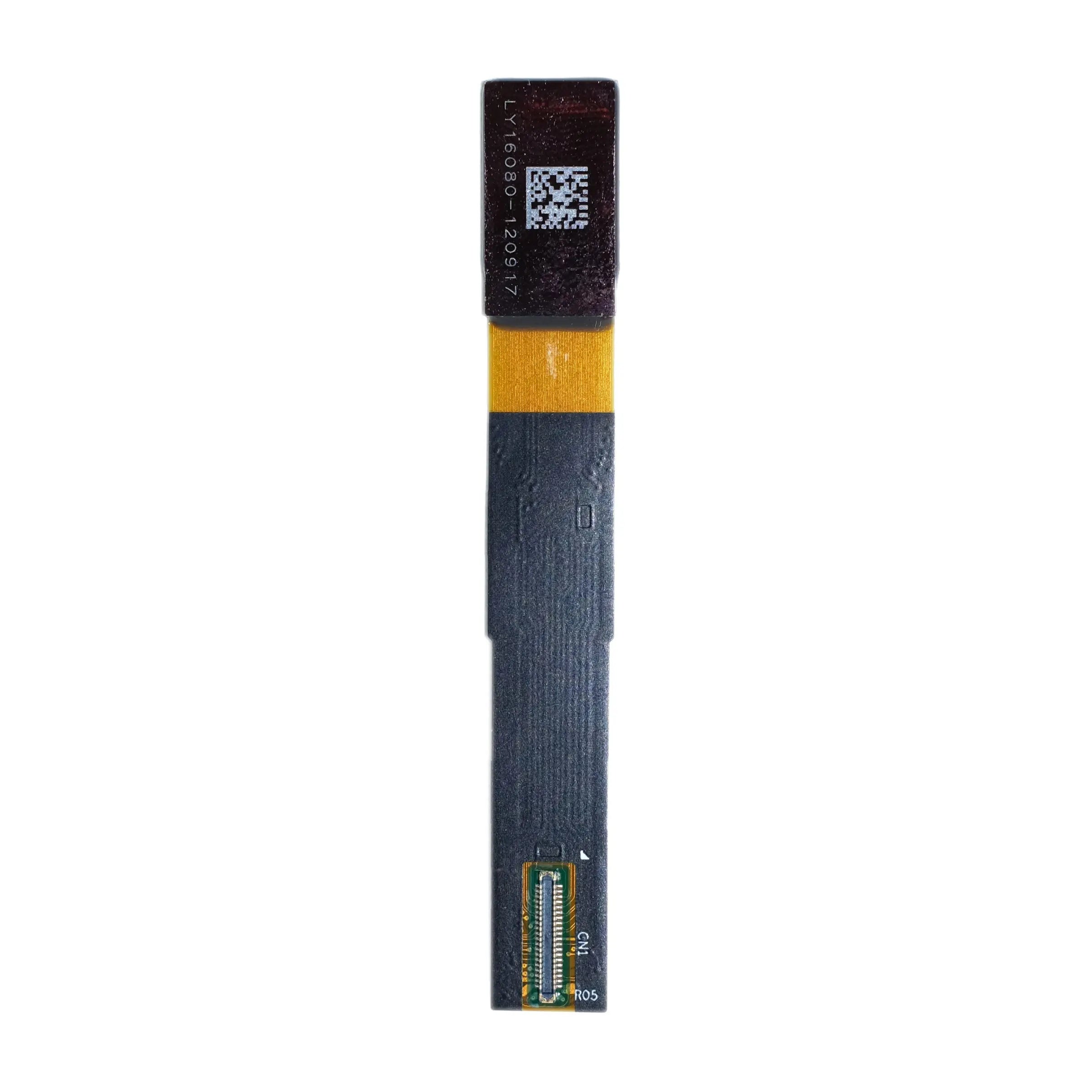
The 2 Wires in the Wiring Diagram:
I²C's biggest selling point is "minimal pins." Take the Adafruit 0.96-inch circular OLED display (model #1947) as an example. Official wiring requires only 2 signal wires:
- SCL to master's I²C clock pin (e.g., Arduino Uno A5)
- SDA to master's I²C data pin (e.g., A4)
- Plus VCC (3.3V), GND (ground), totaling 4 wires (including power)
Compared to SPI's 4-5 signal wires, I²C frees up pins for other peripherals.
Overseas developers making smart chest straps (e.g., Whoop Strap 4.0 prototype) use I²C to connect both the circular display and a heart rate sensor simultaneously, reserving only 2 sets of I²C pads on the PCB.
How Fast Can It Transfer and What Can It Send?
I²C speed has three grades (overseas manufacturer measurements):
- Standard Mode: 100 kbps (12.5 KB/s), most stable, compatible with all devices.
- Fast Mode: 400 kbps (50 KB/s), supported by most modern controllers.
- High-Speed Mode: 3.4 Mbps (425 KB/s), requires both screen and controller support (rare).
But even at the fastest 3.4 Mbps, it cannot transfer image data efficiently. Example for a 128×128 circular display (16-bit color, 256KB/frame):
- 100 kbps: 256KB ÷ 12.5KB/s = 20.48 seconds per frame, frame rate 0.05 fps (barely moving).
- 3.4 Mbps: 256KB ÷ 425KB/s ≈ 0.6 seconds per frame, frame rate 1.67 fps (slideshow).
Therefore, in circular displays, I²C only handles control tasks: sending small commands like "clear screen," "draw pixel," "adjust contrast" (2-5 bytes per command). Image data stays in the screen's GRAM.
Power Consumption:
I²C's low power comes from "no power consumption when not transmitting." Manufacturer measurements (3.3V supply, 25°C ambient):
- Active Mode (transmitting commands): NXP LPC55S69 master + I²C screen, current 0.2-0.3mA (lower than SPI's 0.5mA).
- Idle Mode (master standby, screen on): current 0.05μA (similar to coin cell self-discharge).
- Sleep Mode (screen backlight off): current <0.01μA (near zero).
Compared to MCU Parallel interface (3mA active), I²C is significantly more power-efficient.
The Fitbit Charge 5's circular display status bar (showing battery, steps) uses I²C, extending battery life by 1.5 hours.
Which Devices Use It?
In overseas end-product cases, I²C targets "small screen + multi-sensor integration" scenarios:
- Wearables: Garmin Venu Sq circular display (1.3-inch, 280×280, I²C sends activity mode commands, images stored in GRAM), Withings ScanWatch (medical-grade circular display, I²C connected to ECG sensor).
- Medical Instruments: Philips IntelliVue MX550 monitor (circular status screen, I²C displays heart rate/SpO2, also connected to temperature probe).
- Industrial Control: Red Lion Controls G310 circular HMI (1.5-inch, 128×128, I²C connects to PLC module for alarm commands).
MCU Parallel
How to "Direct Connect" to the Screen?
MCU Parallel mimics the old MCU external bus approach, where the master and screen use a bunch of wires to hand-off data.
The screen itself has no GRAM (Graphics RAM). All pixel colors to be displayed are stored in the master's memory and sent piece by piece to the screen, like building with Lego.
Specifically, it uses these wires:
- Data Lines: 8 (D0-D7) or 16 (D0-D15), transferring 1 or 2 bytes of data at a time (e.g., 16-bit color RGB565, red is 0xF800, sent as F8 and 00).
- Control Signal Lines: WR (write signal, master says "I've placed data here"), RD (read signal, less used), CS (chip select, master says "screen, get ready"), RS (command/data select, 0 for commands like "clear screen," 1 for pixel data).
- Power/Ground: VCC (3.3V/5V), GND (ground).
For example, to send one frame of a 240×240 circular display (16-bit color, 115KB), the master sequentially fetches the 2-byte data for each pixel from memory and sends it to the screen via D0-D15.
The "Ball of Wires" in the Wiring Diagram:
Take the ST STM32F469 Discovery Kit with a 2.1-inch circular TFT display (model L2R2-215) as an example. Wiring requires:
- 16 data lines (D0-D15)
- 4 control signals (WR, CS, RS, RESET)
- 2 power lines (VCC, GND)
- Total 22 wires (including power). Compared to SPI's 4-5 wires, I²C's 2 wires, it's a "ball of wires."
How Fast Can It Run and What Can It Display?
MCU Parallel speed depends on data bus width + bus clock.
16-bit data lines (D0-D15) are twice as fast as 8-bit. Higher bus clock (e.g., STM32's APB bus clock 168MHz) means more data transferred per second.
Measured Data (three overseas controller + circular display combinations):
- ST STM32F407 (168MHz APB clock, 16-bit data lines): Bandwidth = 168MHz ÷ 2 (dual-cycle transfer) = 84 MB/s (theoretical). Actually driving a 480×480 display (16-bit color, 461KB/frame) can achieve ~180 fps.
- TI TM4C123 (80MHz APB clock, 16-bit data lines): Bandwidth = 80MHz ÷ 2 = 40 MB/s. Driving a 320×320 display (205KB/frame) achieves ~195 fps.
- NXP Kinetis K66 (120MHz APB clock, 8-bit data lines): Bandwidth = 120MHz ÷ 4 = 30 MB/s (8-bit is less efficient). Driving a 240×240 display (115KB/frame) achieves ~260 fps (but resolution is limited).
It can drive much higher circular display resolutions than SPI. For example, 720p (1280×720) is not circular, but common circular resolutions like 480×480, 600×600 can easily run at 60+ fps.
Power Consumption:
Power consumption comes from data line driving and screen refresh. Manufacturer measurements (3.3V supply, 25°C ambient):
- Active Mode (transmitting data): STM32F407 driving 480×480 display, current 3-4mA (16 lines switching simultaneously consumes power).
- Idle Mode (screen on but not refreshing): current 1-1.5mA (screen sustaining display consumes power).
- Peak Power (full-screen refresh instant): current surges to 5mA (data lines switch simultaneously), lasting <1ms.
Compared to SPI (0.5mA active), it's indeed more power-hungry, but more efficient than RGB interface (requires external frame buffer, 5-7mA).
Suitable for scenarios requiring high real-time performance and accepting slightly higher power consumption.
Which Devices Use It?
In overseas end-product cases, MCU Parallel targets "high real-time + medium resolution" scenarios:
- Automotive Dashboards: Tesla Model 3's circular speedometer display (320×320, 16-bit color, MCU Parallel connected to NVIDIA Tegra master, 60fps refresh), BMW iX's circular navigation display (480×480, TI Jacinto 6 master).
- Industrial HMI: Siemens SIMATIC HMI KTP700 circular operator panel (7-inch, 800×800, 16-bit color, MCU Parallel connected to S7-1500 PLC), Rockwell Automation PanelView circular status display.
- Avionics: Garmin G3000 cockpit circular map display (640×640, 16-bit color, MCU Parallel connected to PowerPC master).
MIPI DSI
What is MIPI DSI?
MIPI DSI stands for Mobile Industry Processor Interface Display Serial Interface. It's a serial interface specifically for transmitting high-definition video to displays.
Unlike "slow chat" protocols like SPI/I²C, it's like "high-speed express delivery," packaging image data into differential signals (a pair of wires, positive and negative, canceling interference) and sending them rapidly to the screen.
It has two operating modes:
- Video Mode: Directly transmits raw pixel data (e.g., RGB888 image for 1080p). The screen displays it upon receipt, suitable for dynamic video.
- Command Mode: Transmits control commands (e.g., "change page," "adjust brightness") + small amounts of image data (e.g., icons), suitable for static interfaces.
Overseas manufacturers (e.g., NXP, Qualcomm, ST) use it to drive circular AMOLED displays because it balances high definition and thinness.
How Pin-Efficient is the Wiring?
MIPI DSI uses differential pairs for transmission. Each pair includes "positive" (DP) and "negative" (DN) signals, offering strong noise immunity. Common configurations:
- Single Lane: 1 pair of differential data lines (DP0/DN0) + 1 pair of clock lines (CKP/CKN), totaling 4 wires (excluding power/ground).
- Dual Lane: 2 pairs of data lines + 1 pair of clock lines, totaling 6 wires.
- Four Lane: 4 pairs of data lines + 1 pair of clock lines, totaling 10 wires (used for high-end 4K displays).
Compared to MCU Parallel's 22 wires, RGB's 24 wires, MIPI DSI is remarkably "few wires, high power."
For example, NXP i.MX 8M Plus master connected to a 1.9-inch circular AMOLED display (1440×1440) uses a single lane (4 wires), reducing PCB thickness by 0.5mm, suitable for AR glasses.
How Fast Can It Transmit HD?
MIPI DSI speed depends on number of lanes and PHY version (physical layer):
- DSI v1.2: Single lane max 2.5 Gbps (≈312 MB/s), dual lane 5 Gbps.
- DSI v2.0: Single lane 10 Gbps (≈1250 MB/s), supports 4K@60fps.
Measured Data (overseas controller + circular display combinations):
| Controller Model | DSI Version | Lane Count | Measured Bandwidth (Gbps) | Supported Circular Display Parameters | Frame Rate (fps) | Power Consumption (Active) |
|---|---|---|---|---|---|---|
| NXP i.MX 8M Plus | v1.3 | Single Lane | 2.5 | 1440×1440 AMOLED | 90 | 2mA |
| Qualcomm Snapdragon 8 Gen 2 | v2.0 | Dual Lane | 10 | 2160×2160 AMOLED | 60 | 3mA |
| ST STM32MP135 | v1.2 | Single Lane | 2.0 | 1080×1080 TFT | 60 | 1.8mA |
Note: Bandwidth = Lane Count × Per-Lane Rate. Actual frame rate affected by screen response time (AMOLED is 20% faster than TFT).
For example, a 1440×1440 display (16-bit color, 4.15MB/frame). Single lane 2.5 Gbps (312 MB/s) can theoretically transmit 75 frames per second.
In practice, due to screen GRAM write latency, achieving 90fps is possible using "partial refresh" (only updating changed areas).
Which Devices Use It?
In overseas end-product cases, MIPI DSI targets "HD + Thin + Low EMI" scenarios:
- Phone Secondary Displays: LG Wing rotating secondary display (6.8-inch circular, 1440×1440, MIPI DSI dual lane, Qualcomm Snapdragon 765G master), ASUS ROG Phone 6 dual-screen (circular touch secondary display, 1080×1080, MIPI DSI single lane).
- AR/VR: Microsoft HoloLens 2 (circular optical module, 1280×1280, MIPI DSI v2.0 four lane, power 2.5mA), Meta Quest Pro (circular status display, 800×800, NXP i.MX 8M Mini master).
- High-End Automotive Displays: Tesla Model S Plaid passenger entertainment screen (9.4-inch circular, 1920×1080, MIPI DSI dual lane, AMD Ryzen V2000 master), BMW i7 rear seat circular screen (1080×1080, Qualcomm 8295 master).
Ecosystem Dependency:
MIPI DSI isn't plug-and-play. The master must integrate a DSI controller (hardware module), and software uses the vendor's driver library. For example:
- NXP uses MCUXpresso SDK, supporting DSI controller configuration (clock, lane count, timing) for i.MX series.
- Qualcomm uses Snapdragon SDK, providing a "DSI Display Driver" framework compatible with "non-standard timing" of circular displays.
- ST uses STM32CubeMX tool, checking the "DSI Host" peripheral, automatically generating initialization code (e.g., clock division, PHY settings).
Masters without integrated controllers (e.g., Arduino Uno) require bridge chips (e.g., TI DS90UB948 to convert Parallel to MIPI DSI), increasing cost and latency (approx. 5ms).
Processes
The "Processes" for circular LCD display modules refer to the full manufacturing flow, comprising 25+ steps, from glass substrate cutting (laser precision ±0.05mm) to backlight assembly (light guide plate dot density 500-800 per cm²), with temperature and humidity control at each step (23±2°C / 50±5% RH).
Users are concerned with how processes like special-shaped lamination (pressure 0.1-0.3 MPa) and driver bonding (COG yield 99.2%) ensure display uniformity (brightness variation <15%), low defective pixel rate (<0.0003%), and reliability from -40°C to 85°C.
Process Framework
Design Adaptation:
First, use AutoCAD to sketch the circular viewing window, import into SolidWorks to create a 3D model, clearly marking display area diameter (common 1.2-2.5 inches) and bezel width (0.3-0.8mm).
Then use ANSYS Mechanical to simulate cutting stress — input physical parameters of the glass substrate (Corning Eagle XG, thickness 0.4mm, Young's modulus 72 GPa), simulate stress distribution during diamond wheel cutting.
If peak edge stress exceeds 40 MPa, it's prone to chipping, so adjust the cutting path curvature (radius ≥5mm) to reduce stress below 25 MPa.
Use Mentor Graphics Calibre tool for pixel mapping, fitting a standard rectangular pixel matrix (e.g., 240x240) into the circular area, calculating that 12% of edge pixels need truncation, covered with a Black Matrix (BM, using Japan DNP's Black Matrix Paste) to prevent light leakage.
Backlight design uses LightTools optical simulation. The Light Guide Plate (LGP) diameter is 0.5mm larger than the display area, with dots arranged in a radial gradient (center density 800 per cm², edge 500 per cm²) to ensure brightness variation <15%.
Substrate Processing:
Substrate processing involves four steps: cleaning, photolithography, etching, and cutting, all performed in a Class 1000 cleanroom (US FED STD 209E).
- Cleaning: Use an FSI ZETA megasonic cleaner with three tanks — first tank: 2% hydrogen peroxide + 0.5% ammonia mixture (80°C) with 1 MHz ultrasound to remove organic contaminants; second tank: deionized water (resistivity >18 MΩ·cm) rinse; third tank: IPA vapor drying. Finally, inspect particles using a Nikon AOI optical inspection system, requiring <0.1μm particle count ≤5 per cm².
- Photolithography (TFT Array): Coat glass with photoresist (Tokyo Ohka Kogyo TOK TSMR-V3), thickness 1.2μm. Expose using a Nikon NSR stepper (wavelength 365nm, energy 120 mJ/cm²). Develop using 2.38% tetramethylammonium hydroxide solution. Etch using aluminum etchant (phosphoric acid:nitric acid:acetic acid = 75:5:20) to pattern the gate (thickness 0.3μm) and source/drain electrodes (molybdenum-niobium alloy, thickness 0.2μm). Line width accuracy ±0.3μm, overlay error measured with KLA-Tencor Archer 600, requiring <0.5μm.
- Circular Cutting: Use a Coherent AVIA UV laser cutting machine (wavelength 355nm, power 10W, pulse frequency 50 kHz), speed 300 mm/s. After cutting, measure edge roughness with a Veeco Wyko NT9100 white light interferometer, requiring Ra <0.1μm for qualification. Cutting margin is 0.1mm (vs. 0.3mm for rectangular displays) because circular shapes have more concentrated stress; a smaller margin saves material.
Module Assembly:
Assembly involves three parts: liquid crystal cell, backlight unit, and driver bonding, like building Lego but with controlled force and temperature at each step.
- Liquid Crystal Cell: Coat inner surfaces of TFT glass and CF glass (Japan Toppan CF-123) with polyimide alignment film (Japan Synthetic Chemical SE6511) using a Canon coater (gap control ±0.5μm), bake at 130°C for 60 minutes. Rubbing uses a Tokyo Electron rubbing machine, with Teijin ES301 nylon cloth, rotation speed 500 rpm, travel 10 mm, pretilt angle adjusted to 88°±1°. Liquid crystal uses Merck MLC-2048 (dielectric constant ε∥=12.5). Use Epson PrecisionCore inkjet head (5 pL droplet) for vacuum injection (vacuum <10⁻³ Pa), dispensing 6 μL per cell. Bubbles with diameter >5 μm are rejected. Lamination uses a Tokyo Electron CELLOS vacuum laminator, pressure 0.2 MPa, temperature 25°C. Alignment marks recognized by CCD (accuracy ±2 μm). Cell gap tolerance ±0.01 mm (measured with Micromap 570).
- Backlight Unit: Light Guide Plate uses Sumitomo Chemical PMMA (refractive index 1.49), diameter 30mm, molded using an Arburg injection molding machine (barrel temperature 220°C). Surface dots engraved with Trumpf laser (diameter 80 μm, spacing 200 μm, density 600 per cm²). LEDs selected are Seoul Semiconductor WICOP SN3 (color temperature 6500K, luminous flux 25 lm), 6 pieces placed along the LGP circumference, spacing 45°, drive current 20 mA each. Optical films use 3M BEF II diffuser (transmittance 92%) + LG Chem DBEF brightness enhancement film (gain 2.5x). Cutting uses a Zünd G3 L-2500 CNC cutter, tolerance ±0.2mm.
- Driver Bonding: Driver IC uses TI SN65DSI86 (supports MIPI DSI). COG bonding uses Hitachi ACF AC-7206U-18 (conductive particle diameter 5 μm). Hot press settings: temperature 190°C, pressure 10 N per point, time 10 seconds. Post-bonding resistance <50 mΩ (measured with Keithley 4200). COF uses DuPont Pyralux AP9121R (thickness 0.1mm), bend radius R=1.5mm (> minimum bend radius 1mm). 5000 cycles of ±90° bending test using Instron 5944 tensile tester, conductivity >99.9%.
Testing and Calibration
Using Machine Vision to Clearly See Brightness, Darkness, and Color
- Brightness Uniformity: In a dark room (illuminance <0.1 lux, verified with Extech LT300 light meter), set up a Konica Minolta CS-2000 spectroradiometer, lens aimed at screen center. Then scan at 8 equally spaced points along the radius (0.4 times radius from center), totaling 9 points. Take three measurements at each point and average. For example, for a 1000-nit screen, the lowest point must not be below 850 nits (uniformity >85%). Pay special attention to edge points — circular display edges are prone to darkening. If any point's brightness is more than 20% lower than the center, check the backlight LGP dot density.
- Color Accuracy: Use an X-Rite Ci64 imaging colorimeter to capture the full screen, generating a CIE 1931 color coordinate diagram. According to sRGB standard, white point coordinates must be within (0.3127, 0.3290) ±0.005. Red, green, blue primary color coordinate deviation Δu'v' <0.015 (use CIE ΔE*ab <2 for auxiliary judgment). For example, Seoul Semiconductor WICOP LED has a color temperature of 6500K. If measured deviation exceeds 200K, adjust the drive current (20 mA per piece ±0.5 mA).
- Defective Pixel Screening: Use a Radiant Vision Systems ProMetric I series camera (29 megapixels) to capture the full screen. Judge according to ISO 13406-2 Class II standard: total number of bright pixels (brightness >2x background), dark pixels (brightness <0.5x background), and colored pixels (abnormal RGB channels) <0.0003%. A 1.3-inch screen (240x240 pixels) allows a maximum of 1 defective pixel; a 2.5-inch screen (454x454 pixels) allows a maximum of 3. Use a ring light source (uniformity >95%) with the camera to avoid false positives from reflections.
Measuring Circuit Current, Voltage, and Response Speed
Electrical testing uses source meters and oscilloscopes to examine the circuit's "fundamentals," checking for pixel leakage, response speed, and interface stability.
- Pixel Response Time: Use a Keithley 2602B source meter to apply 5V drive voltage to a pixel. Capture signal rise time (10% → 90%) and fall time (90% → 10%) with a Tektronix DPO7000 oscilloscope. Requirements: rise/fall time both <10 ms.
- Leakage Current: Again using the 2602B, measure pixel current after turning off the drive voltage. Requirement: <0.1 pA per pixel (picoamp level). High leakage current causes screen flicker, especially noticeable at low temperatures (-20°C).
- Interface Signal: Connect a Keysight DSOX1204G oscilloscope to the MIPI DSI interface, measure eye diagram opening — using PRBS7 pseudo-random signal, at 1 Gbps rate, vertical eye opening >0.7 UI (Unit Interval), horizontal eye opening >0.6 UI.
Simulating Extreme Environments to See If It Can Withstand
Reliability testing subjects the screen to harsh conditions per international industrial standards to see if it fails over time.
- High Temperature & Humidity: Use a Thermotron T-48CH constant temperature and humidity chamber set to 85°C/85% RH for 1000 hours (~42 days). Remove and test every 168 hours: brightness attenuation <10%, defective pixel increase <0.0001% (for a 1.3-inch screen, this is an increase of at most 0.0000026 pixels, practically undetectable), FPC conductivity >99.5% (measure loop resistance <1Ω with Fluke 117 multimeter).
- Thermal Shock: Use an ESPEC PL-3J rapid thermal cycling chamber, switching between -40°C ↔ 85°C, holding each temperature for 30 minutes, 500 cycles (~21 days). Measure cell gap change <0.005 mm (using Micromap 570), check for no liquid crystal layer separation (viewed with polarized microscope).
- Vibration & Drop: Use a Lansmont TV550 vibration table per MIL-STD-810H standard, frequency sweep 5-500 Hz, acceleration 5G, duration 2 hours. Then use a Drop Test Machine to drop from 1.2 meters height onto a steel plate (once on each of 6 faces). Afterwards, inspect for glass cracks (using Olympus BX53 microscope to check edge micro-cracks) and FPC solder joint detachment (test connectivity with Hioki FA1240 flying probe tester).
En lire plus
LCD backlights are divided into two types: LED and CCFL. LEDs are the mainstream technology, with a lifespan of 50,000+ hours, 30%-50% lower power consumption than CCFLs, a color gamut of 95%+ sRGB...
When selecting a reliable LCD module supplier, focus on qualifications, production capacity, quality control, and service. Check for ISO 9001/IATF 16949 certification, prioritize automotive-grade ...
Laisser un commentaire
Ce site est protégé par hCaptcha, et la Politique de confidentialité et les Conditions de service de hCaptcha s’appliquent.