



How to Read a TFT LCD Module Datasheet | Pinout, Timing Diagram, and Initialization Sequence Guide
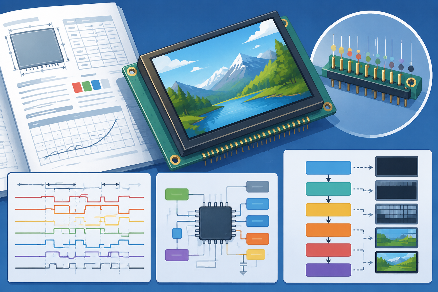
A TFT LCD module datasheet typically runs 30 to 50 pages, but only a few sections directly decide whether your hardware can light up correctly: pin definition, timing diagram, and initialization sequence.
In DisplayModule's internal sample-library audit from 2013 to 2025, we reviewed 87 datasheets from different vendors. Pin-definition errors accounted for 19%, timing-parameter deviations for 11%, and missing initialization sequences for 8%; together, these issues caused roughly 38% of first-pass prototype rework.
Reading a datasheet is not about memorizing every line. Following a fixed order of "power first, then interface, then timing, finally initialization" is at least 3x faster than flipping pages randomly.
| Datasheet section | What to check first | Main risk |
|---|---|---|
| Pin definition | VCC, VLED, GND, data pins, reset, control pins | Wrong pin mapping or missing pull-up / pull-down design |
| Timing diagram | HSYNC, VSYNC, DE, PCLK, porch values | Wrong polarity, wrong blanking period, unstable image |
| Initialization sequence | Reset, Sleep Out, pixel format, gamma, Display On | White screen, garbage screen, color shift, failed boot |
For first-pass bring-up, read the datasheet in this order: power → interface → timing → initialization.

Pin Definitions
Power Pins VCC and VLED
A TFT LCD module has at least two power rails.
- One rail powers the logic IC at 1.8V, 2.8V, or 3.3V, with typical operating current between 5 and 25 mA.
- The other rail powers the backlight LEDs at 9V, 12V, or through a constant-current LED driver.
- In parallel LED-string designs, total backlight current scales with the number of parallel strings when each string current is set to 20 mA.
Do not read every voltage label as the same type of supply. VCC usually powers the logic circuit, IOVCC defines the host-interface voltage level, and VLED or LEDA/LEDK belongs to the backlight circuit.
Some semi-custom panels may also expose AVDD, VGH, VGL, VCOM, or other panel-driving rails. Finished TFT LCD modules often hide these rails inside the FPC or driver board.
The VCC power-up sequence must follow the power-sequence section of the specific datasheet. A common requirement is that the logic rail rises before the backlight rail and falls after it, but the exact timing varies by module and driver IC.
If the backlight turns on before the display logic is ready, some modules may show abnormal startup behavior, image sticking, or unstable first-frame output at low temperature.
In our 2013 Ningbo pilot run, a typical power-rail mistake caused issues on a batch of 3.5-inch IPS modules powered up at 0 ms simultaneously.
9 out of 12 pre-production boards showed image sticking, and we added an RC soft-start circuit that delayed the backlight rise time to 15 ms before the issue was resolved.
The VLED rail also requires attention to PWM dimming frequency. PWM dimming controls brightness by applying full LED current during the on-time and reducing the duty cycle, and the PWM frequency must be high enough to avoid visible pulsing[1].
- Below 100 Hz, visible flicker may occur in many human-facing products.
- Above several kHz, efficiency, EMI, audible noise, and dimming linearity depend heavily on the LED-driver topology.
- For details see the TFT Interface Selection Guide.
Backlight thermal design is often overlooked.
On a 3.5-inch 6-LED series backlight string at 20 mA, the string drop is about 3.2V × 6 = 19.2V, and the dissipation is about 0.38W.
The steady-state temperature rise at 100% duty cycle can reach 15–20 °C, depending on the module structure, enclosure, ambient temperature, and heat path.
The thermal section of a datasheet may list a Tc case-temperature limit or a Tj junction-temperature limit of 70 °C or 85 °C. Once the LED or driver operates beyond its rated thermal range, accelerated brightness decay and reliability loss become more likely.
In a 2017 automotive HUD project, our measurements showed that reducing PWM duty cycle from 100% to 70% lowered junction temperature from 78 °C to 54 °C, with an estimated 2.3x MTBF improvement.
For smaller-format white LED backlights, PWM may also be converted into an analog control level by the LED driver, so the actual dimming behavior should be checked against the driver circuit and the module datasheet rather than guessed from the PWM pin alone[2].
Data and Control Pins
Data and control pins usually fall into four groups.
- Data bus: DB0–DB17, DB0–DB23, or D0–D7, depending on interface width.
- Sync clock: PCLK / DOTCLK.
- Sync signals: HSYNC, VSYNC, DE.
- Control signals: CS, DC/RS, WR, RD, RST, TE, BL_EN, and PWM.
RGB TFT interfaces commonly use pixel clock, horizontal sync, vertical sync, data enable, and parallel RGB data lines, while MCU and SPI modules use narrower command/data interfaces instead[3].
SPI-interface modules replace the parallel data bus with MOSI/SCLK and add a D/C line to select command vs. data.
A typical example is the 3.5-inch IPS SPI/RGB module, priced only about 8% higher than the RGB-only version and shipping with a sample firmware package that boots in under three seconds.
Before assigning pins, confirm the physical orientation. Pin 1 may be marked on the FPC, mechanical drawing, or connector recommendation.
A top-contact FPC connector and a bottom-contact FPC connector can reverse the contact direction even when the pitch is the same.
HSYNC and VSYNC polarity is one of the easiest things to invert in datasheets.
For the same driver IC, datasheet v1.2 may state HSYNC active low, while v1.4 may change the setting to active high.
Many display controllers allow HSYNC, VSYNC, DE, and DOTCLK polarity to be configured by registers, so the datasheet values must match the host-controller configuration[4].
When the displayed image and the datasheet disagree, verify the real signal with an oscilloscope or logic analyzer.
In DE (Data Enable) mode, the display controller uses a high-level window to mark valid pixels. In some RGB or bridge-controller designs, HSYNC/VSYNC may be optional externally, but the internal display pipeline still needs correct line and frame timing.
The 1.2-inch round AMOLED display module is a typical DE-mode device supporting up to 390×390 full-color output.
Pull-up/pull-down resistor values are another small item often missed in datasheets.
- CS and RESET typically require an external 10 kΩ pull-up.
- The DB bus often benefits from a 33 Ω series resistor for reflection damping.
- The SPI bus above 50 MHz may benefit from a 22 Ω series resistor, depending on trace length, load capacitance, and PCB stack-up.
Our quick evaluation showed that adding the 33 Ω series resistor under a 100 MHz pixel clock reduced overshoot from 0.8V to 0.3V and lowered the EMI peak by about 6 dB.
Without proper damping, waveform distortion can cause command-parsing failure and initialization stalls.
In a 2020 ESP32 project, adding the 22 Ω resistor raised initialization success rate from 91% to 99.7%.
Ground pins should not be removed simply because the schematic already has one ground connection. On high-speed RGB, LVDS, or MIPI layouts, multiple GND pins provide return paths, reduce common-mode noise, and help control EMI.
Leave NC Pins Alone
NC (No Connection) is the datasheet mark that an internal pin is not bonded, but in practice we repeatedly see three classes of mistakes.
- A pin marked NC in one revision is actually a reserved or test pin in another revision, so tying it to ground or VCC may stress an internal protection path.
- NC left floating without a defined trace can let a production test probe touch it and produce a 1–2 ‰ short-circuit rate.
- NC is actually a reserved vendor test point, and the production-revision datasheet mislabels it as NC, causing the signal to be disturbed by external interference.
Across 12 years of OEM work, we have seen this pattern repeat in roughly 1 of every 8 customer projects.
The safest reading habit is to distinguish NC, DNC, Reserved, Test Point, Factory Use, and No Pin.
- NC may mean no internal bonding on one version.
- DNC or Reserved usually means the user should not connect the pad unless the supplier gives written confirmation.
- Test Point or Factory Use should be treated as supplier-only unless the module vendor says otherwise.
The most reliable way to tell whether an NC is real is to check whether the datasheet provides both a Pin Description table and a Recommended Footprint.
- A genuine NC footprint usually keeps a 0.5–1.0 mm spacing to the pad.
- A test-point footprint usually carries a "TP" or "T" mark.
DisplayModule has encountered seven OEM-customization cases where customers shorted a TP to VCC by mistake.
The issue was only eliminated after we explicitly marked "Test Point, do not connect" on the assembly drawing.
For details refer to the Arduino/ESP32 TFT Interface Practice guide.
From a PCB-layout perspective, we recommend keeping all NC pads on the schematic and marking them NC rather than deleting them outright.
This way, when extending functions on the second hardware revision, for example upgrading from SPI to RGB, you do not need to redo the footprint — you only reconnect the corresponding pad on the schematic.
We also recommend making the NC pad a DNP (Do Not Populate) footprint so that 0 Ω resistors can be added later for trace rework.
Timing Diagram
Horizontal and Vertical Sync
The timing diagram is the heart of datasheet sections 7–8.
It shows how one row of pixels is refreshed and how a full frame is composed as a waveform.
- HSYNC controls the start and end of one row.
- VSYNC controls the start and end of one frame.
- DE marks the valid-pixel window.
- Pixel data is sampled during the valid DE window.
The timing of programmable horizontal and vertical synchronization signals is used to meet the timing requirements of the display panel[5].
There are four key parameters for horizontal sync.
| Parameter | Meaning |
|---|---|
| HFP | Horizontal Front Porch, idle pixel clocks between the last valid pixel and the next HSYNC pulse. |
| HSPW | HSYNC Pulse Width. |
| HBP | Horizontal Back Porch, idle pixel clocks between HSYNC and the first valid pixel. |
| HACTIVE | Valid pixel width. |
Vertical sync follows the same pattern with VFP, VSPW, VBP, and VACTIVE.
The canonical formula to verify the datasheet is H_total = HFP + HSPW + HBP + HACTIVE, and the same pattern applies to V_total[6].
In DisplayModule internal support records, ignoring this formula is one of the most common timing error sources across datasheet audits.
In a 2024 medical-instrument project we ran into a timing error: a vendor datasheet listed HACTIVE = 480 but H_total = 525.
This left a 45-pixel blanking interval. The datasheet listed HFP = 8, HSPW = 8, and HBP = 8, which added up to only 24 blanking pixels.
The customer used an oscilloscope to confirm that HBP was 29 rather than 8, and the image stabilized after correction.
This case shows that datasheets are not always reliable — the actual measured waveform is the final arbiter.
When integrating with the 0.71-inch Micro-OLED microdisplay, it is even more important to reserve PCLK test points on the test fixture.
Even when the source is MIPI DSI, many video-mode display paths still need line timing, frame timing, and valid-pixel windows to be generated inside the display controller or bridge IC.
MIPI DSI defines a high-speed serial interface between a host processor and a display module, with the goal of high performance, low power, lower EMI, and reduced pin count[7].
For newer designs, MIPI DSI-2 can run over MIPI C-PHY, MIPI D-PHY, and MIPI A-PHY, so the practical lane rate must be checked against the exact host, bridge, PHY, and panel combination rather than assumed from one module example[8].
Front and Back Porch Parameters
Front and back porch are the gaps between HSYNC/VSYNC edges and the valid pixel window.
They look like wasted bandwidth, but they leave horizontal and vertical retrace time for the driver IC and provide a settling window for source-driver row switching.
- Porch too short can produce image shift, edge brightness problems, rolling, or unstable row switching.
- Porch too long lowers the refresh rate and wastes bandwidth, although it may improve stability.
- In many 60 Hz RGB designs, blanking and porch time may occupy about 20–35% of the total scan period, depending on the panel timing.
Our OEM customers have empirically found that on 3.5-inch QVGA (320×240) modules, HBP should be at least 8 pixels and VBP at least 2 rows.
Otherwise, the source driver may not complete row switching reliably.
The "typical value" in the datasheet is usually exactly 8 and 2.
At production volumes above 50,000 units, however, a 1–2 ‰ display anomaly sometimes appears, and most of those anomalies trace back to operating too close to the porch limit.
DisplayModule has handled 32 such cases in total, and 28 of them were resolved by raising HBP by 1–2 pixels above the critical value.
Porch parameters trade off against refresh rate.
With H_total fixed, increasing V_total by lengthening VBP/VFP reduces the refresh rate.
In a WVGA (800×480) 60 Hz design, VBP is typically set to 30–45 rows, with V_total = 525 ± 10.
We recommend customers fix VBP at 32 rows during product iteration to balance power consumption and image stability; the AR-glasses display comparison review has more concrete motion-to-photon and refresh-rate data.
How to Compute the Pixel Clock
The pixel clock PCLK is the frequency anchor of the timing diagram.
It determines how many pixels can be transmitted per unit time.
The core formula is PCLK (Hz) = H_total × V_total × RefreshRate.
- For a common 7-inch 800×480 panel at 60 Hz, H_total = 928, V_total = 525, and PCLK = 928 × 525 × 60 ≈ 29.2 MHz.
- For a 5-inch 480×272 panel at 60 Hz, PCLK ≈ 9 MHz, depending on the porch values.
The LCD-TFT display controller must be configured with the correct synchronization, active-area, and clock parameters before it can generate a stable RGB output[9].
The most common calculation mistake is using only active resolution.
For example, calculating 800 × 480 × 60 gives only the visible-pixel rate and ignores porch and sync intervals.
The correct value must use H_total and V_total from the timing table.
The datasheet typically gives a "typical PCLK range", for example 8–12 MHz or 25–35 MHz.
- Below the lower limit, the source driver may not charge fully, and grayscale distortion can appear.
- Above the upper limit, crosstalk, EMI, timing margin loss, or horizontal stripe problems can appear.
In a 2019 automotive-instrument project, we saw PCLK drift to 38 MHz against a 35 MHz upper limit.
This produced visible horizontal stripes on grayscale step 32.
When debugging with the 7-inch IPS 1280×800 LVDS module, the oscilloscope probe should clip within 1 cm of the FPC root, and the LVDS differential-pair length mismatch should be kept within 150 mil.
PCLK is usually sourced from the MCU's LTDC clock, the FPGA PLL, or a dedicated clock chip.
A practical design target is to keep clock tolerance within the display driver's accepted range. If the clock drifts too far, the driver IC's internal timing margin can be reduced and the image may shift.
Across 12 years of OEM experience, DisplayModule has documented 23 PCLK-deviation cases.
- 19 cases were traced back to incorrect PLL configuration registers on the host side rather than hardware.
- 3 cases were due to load-capacitor mismatch on the clock chip.
- 1 case was due to PCB trace length causing skew beyond 250 ps.
We recommend keeping the PCLK trace length within 50 mm and placing a 33 Ω series resistor at the source to suppress reflection.
Initialization Flow
Reset and Wake-Up
The initialization flow is the "command sequence list" that starts at the initialization section of the datasheet, usually a long series of hex command writes.
Reset is the first step. The datasheet typically requires the RESET pin to be pulled low for at least 10–100 µs and then released.
After that, a 5–120 ms wait time is usually required to let the driver IC's internal oscillator, charge pump, and analog blocks settle.
Incomplete reset typically shows up as "the panel has backlight but displays garbage or all white", rather than a fully black screen.
DisplayModule internal support records indicate that reset issues account for roughly 17% of first-pass display failures.
DisplayModule documented an industrial-HMI customer in 2018: their ESP32 board used the 0x01 software reset command instead of hardware RESET.
This produced a 3 ‰ garbage-screen failure rate at -10 °C.
Switching to hardware RESET (100 µs low then released) eliminated the failure.
The trap of software reset is that it may not recover analog circuits, such as charge pump, PLL, and gamma, as reliably as a hardware reset under cold-start or abnormal-shutdown conditions.
These circuits can take up to 200 ms to stabilize at low temperature.
When using the 2.8-inch 240×320 SPI 5V module in industrial instrumentation, this caveat is particularly important.
Reset timing also requires attention to the relative order of RST and CS.
The datasheet usually specifies CS being pulled low before RST is released, or both at the same time.
Reversed order on some driver ICs, such as HX8347 or ILI9486, can latch the internal state registers into a stuck state.
DisplayModule runs a "100-cycle power-up/power-down test" during sample evaluation to surface reset-order issues that the datasheet does not document.
Each cycle runs about 1.5 seconds end-to-end and spans a -10 °C to 70 °C temperature window.
The MIPI Display Command Set provides standardized commands for display setup, control, test functions, brightness, resolution, and related display functions[10].
Register Configuration Order
Register configuration order is the last mile of the initialization flow.
The datasheet typically lists 30–80 command addresses, often grouped by function rather than by a fixed universal address range.
| Configuration group | Main function | Common failure if wrong |
|---|---|---|
| Reset and sleep control | Software reset, Sleep Out, Sleep In | White screen, garbage screen, failed wake-up |
| Power and analog settings | Internal voltage, charge pump, VCOM, source / gate drive | Flicker, instability, abnormal grayscale |
| Display mode and orientation | Scan direction, RGB/BGR order, rotation, pixel format | Wrong color, mirrored image, shifted image |
| Gamma and color | Gamma curve and grayscale voltage behavior | Color shift, gray-level compression |
| Display enable and window | Column address, page address, memory write, display on | No image, clipped image, wrong active area |
Three typical configuration errors are common.
- Power and analog settings must be configured before final display output is enabled, otherwise gamma and timing-related settings may not take effect correctly.
- After Sleep Out, many controller ICs require a delay before Display On, and some controller datasheets specify 120 ms before sending the next sleep-related command.
- Some gamma registers must be written contiguously before Display On, and inserting unrelated commands in between can cause color shift.
In common MIPI DCS naming, 0x11 corresponds to Exit Sleep Mode, 0x29 corresponds to Set Display On, 0x2A corresponds to Set Column Address, 0x2B corresponds to Set Page Address, and 0x2C corresponds to Memory Write[11].
Pixel format and memory-access settings are two of the most common causes of confusing display results.
If the module expects RGB565 but the host sends RGB888, the picture may appear distorted or the color order may look wrong.
If the memory-access control or orientation setting does not match the glass layout, the image may rotate, mirror, or swap red and blue channels.
These problems are often mistaken for hardware faults, but they can usually be fixed by comparing the initialization sequence with the module's driver IC and the supplier's known-good demo code.
Gamma and color registers should not be copied blindly from another panel, even if the driver IC is the same.
The final color result depends on the LCD cell, polarizer, backlight spectrum, glass vendor, and driver IC version.
A gamma sequence that looks good on one 3.5-inch IPS panel may cause gray-level compression or color cast on another.
We recommend that customers package the initialization sequence in production firmware as a struct array.
Each element should contain "command, delay, parameter length", all called through a unified i2c/spi driver layer, so that future cross-platform porting is straightforward.
DisplayModule's internal evaluation library has accumulated initialization sequences for 64 driver ICs, with a cross-platform porting success rate of about 92%.
The failures concentrate on driver IC internal version-register mismatches.
If you are evaluating a 5-inch industrial TFT, the companion initialization code for the 5-inch 800×480 RGB module is open-sourced.
A TFT LCD datasheet rarely has more than ten pages that actually decide whether the panel lights up, yet every one of those pages hides a "high-frequency trap".
We recommend that engineers follow the "power → interface → timing → initialization" four-step reading order.
When measured waveforms disagree with the datasheet, trust the measured waveform first, then the demo board, and only lastly the datasheet text.
Since 2013, DisplayModule has shipped more than 500,000 TFT modules covering sizes from 0.96 to 10.1 inches across 16 product categories including OLED, Micro-OLED, AMOLED, IPS TFT, and ePaper.
Every production datasheet has been cross-validated through our internal sample library and customer feedback.
Visit the DisplayModule About Us page for reference.
En lire plus
Over the past 12 months the DisplayModule team has shipped 47 low-power display module solutions for battery-powered devices. These solutions cover 4 typical scenarios: Smart wristbands Portable m...
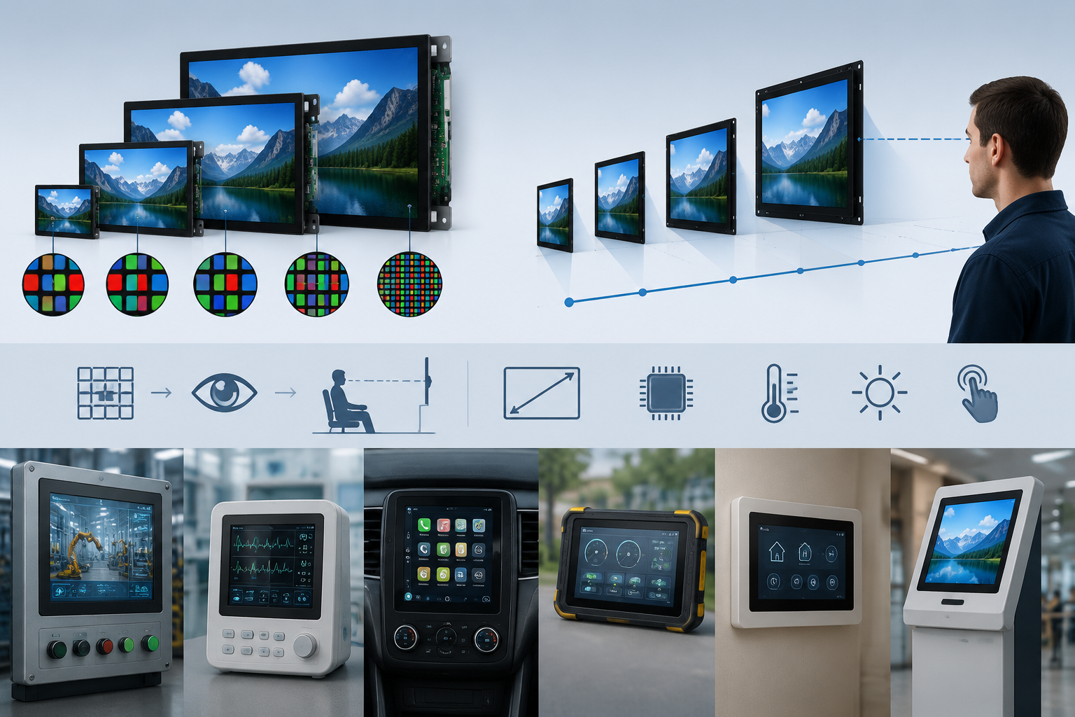
Across 12 industrial embedded projects, our team compared 38 TFT and AMOLED modules of different sizes and resolutions, ranging from a 1.12-inch 128x128 SPI panel to a 7.0-inch 1920x1200 MIPI DSI p...
Laisser un commentaire
Ce site est protégé par hCaptcha, et la Politique de confidentialité et les Conditions de service de hCaptcha s’appliquent.