


Micro OLED vs Standard OLED | Silicon Substrate, Resolution & Price
Micro OLED uses a monocrystalline silicon substrate, replacing the glass or plastic substrates of standard OLEDs, allowing its resolution to easily break through 3000 PPI, far exceeding the 500 PPI of standard versions, effectively eliminating the screen door effect in VR devices.
However, its per-piece cost is often as high as $300, several times the $50 manufacturing cost of the standard version, and it is currently only used in high-end headsets.
Silicon Substrate
Standard OLEDs use glass substrates. Limited by manufacturing processes, the pixel pitch is usually greater than 50 microns.
Micro OLED switches to 8-inch or 12-inch semiconductor monocrystalline silicon wafers. Through TSMC's or GlobalFoundries' CMOS shrinking processes, the control circuit is photolithographed directly onto the silicon wafer.
The physical size of sub-pixels is reduced to 4 microns, and the aperture ratio of the light-emitting area is increased to 80%, allowing a 0.4-inch area to output full HD pictures, and the physical volume of the screen module is simultaneously reduced by 60%.
Farewell to the Grid Image
The optical lenses of headset devices physically magnify the image of the bottom screen by 10 to 20 times. When the lenses are aligned with conventional glass-substrate OLEDs, the originally tiny pixel gaps are also magnified by the same multiple. Limited by the manufacturing tolerances of Fine Metal Masks (FMM), the physical pixel pitch on glass substrates is usually limited to more than 50 microns.
FMM is prone to gravity sag and thermal expansion or contraction during the high-temperature evaporation process, and physical position errors often reach 2 to 3 microns. To prevent color crosstalk between adjacent red, green, and blue sub-pixels, panel factories reserve wide black physical isolation bands between sub-pixels. These large-area isolation bands occupy the physical space that originally belonged to the illuminants.
The ratio of the light-emitting area to the total pixel area is called the aperture ratio. The aperture ratio of glass panels usually stagnates in the 20% to 30% range. When the naked eye observes the screen through magnifying lenses, up to 70% of the area in the field of view is a non-illuminating black grid. The black grid acts like a dark screen door covering the picture, destroying the optical immersion of the 3D virtual environment.
The physical bottlenecks limiting the pixel density of glass substrates include:
-
The lower limit of the metal mask thickness is stuck at 10 to 15 microns.
-
The thermal expansion coefficient of glass causes the evaporation alignment deviation rate to be higher than 5%.
-
The effective light-emitting aperture ratio cannot break through the physical upper limit of 30%.
-
The transistor yield rate drops off a cliff after the screen PPI reaches 600.
After replacing the bottom carrier with an 8-inch or 12-inch semiconductor monocrystalline silicon wafer, the old FMM evaporation equipment is completely abandoned. Wafer foundries like GlobalFoundries and Tower Semiconductor begin to take over screen manufacturing, using mature 90nm or 28nm extreme ultraviolet lithography machines to engrave extremely tiny pixel control circuits onto monocrystalline silicon.
The processing accuracy of the semiconductor lithography process is at the nanometer level, far exceeding the micron-level physical lower limit of metal masks. On monocrystalline silicon wafers, R&D personnel forced the physical size of the light-emitting sub-pixels to be compressed to below 4 microns. The physical isolation band between two adjacent sub-pixels is drastically reduced to an extremely small range of 0.1 to 0.5 microns.
The transistor circuit layout on the silicon substrate is extremely compact, and the utilization rate of the underlying 3D space multiplies. The aperture ratio of the light-emitting layer of Micro OLED easily breaks through the 80% manufacturing threshold. The thick black isolation bands that originally lay between the pixels completely disappear, and the pixel density of the screen increases exponentially.
The 0.7-inch silicon-based OLED panel mass-produced by Sony provides an excellent data reference. Within an extremely tiny monocular display area, 1920x1080 physical light-emitting pixels are densely packed on the silicon substrate. The physical pixel density (PPI) of the panel is as high as 3147, numerically more than five times higher than the screens of regular flagship mobile phones on the market.
Bottom-level optical index changes brought by silicon substrate technology:
-
The physical arrangement pitch of red, green, and blue sub-pixels is reduced to 4 microns.
-
The physical isolation band value of adjacent pixels drops to 0.1 microns.
-
The effective light-emitting area proportion of a single pixel crosses the 80% threshold.
-
The PPI index of micro panels fully covers the 3000 to 4000 range.
-
Only a 1.4-inch silicon wafer area is needed to accommodate 4K-level physical resolution.
The resolution limit of the human retina at a normal viewing distance is about 60 PPD (pixels per degree of field of view). The PPD data of early Oculus Rift devices was only around 10, and the grid sensation observed by the naked eye was extremely severe. After headsets equipped with silicon-based panels are combined with specific Pancake folded optical paths, the PPD index crosses 20 and marches toward 40, exceeding the physical limit of the naked eye to distinguish individual pixels.
The custom Micro OLED panel equipped on the Apple Vision Pro is cut from two stamp-sized silicon wafers. A total of 23 million physical pixels are arranged on the two silicon wafers, and the pitch of a single pixel is extremely strictly compressed to 3.3 microns. Even after strong magnification through a complex three-piece lens module, the visual feedback remains a single, smooth, and continuous picture.
In addition to the mature scheme of white OLED paired with color filters (WOLED+CF), the monocrystalline silicon substrate also supports the more cutting-edge filterless patterned (dPd) technology. The American manufacturer eMagin utilizes the high current-carrying capacity of the silicon substrate, removes the color filter layer that absorbs 70% of light, and achieves an initial brightness output of 10,000 nits at a pixel pitch of 9.3 microns.
The silicon-based backplane designed by Kopin adopts a double-layer OLED vertical stacked structure. The underlying CMOS circuit is responsible for delivering high-voltage working current to both layers of illuminants simultaneously. While maintaining a high brightness of 5000 nits, it renders pictures at lightning speed with a physical refresh rate of 120Hz, eliminating physical motion blur in high-speed motion scenes.
Experience changes brought by the disappearance of the picture grid sensation:
-
Tiny text of 8pt size in the virtual space can be clearly read.
-
Jagged artifacts no longer appear at the edges of high-contrast pictures.
-
The black physical isolation grid under a pure white background completely disappears.
-
The stereoscopic depth perception of microscopic material textures is improved by 40%.
The physical manufacturing cost of monocrystalline silicon wafers is positively correlated with the area value. A 12-inch monocrystalline silicon wafer can roughly only be cut into about 100 1.3-inch panels. Assuming that the defective rate of edge etching in wafer foundries is below 10%, the mass production material cost of a single screen still exceeds $300.
Drastic Reduction in Wearing Weight
When using conventional glass-substrate OLEDs, a wiring area of 3 to 5 millimeters must be reserved at the edge of a single panel. Glass substrates cannot etch complex logic microcircuits, so the huge chip array driving the screen to emit light is forced to hang outside the display area.
A 6-inch standard OLED panel needs to be equipped with an independent display control chip, timing controller, and power management chip. External components are usually soldered onto a printed circuit board with an area of 15 square centimeters and establish a physical connection with the panel through several flexible flat cables.
The physical stacking of external components occupies more than 20% of the internal space at the front end of the headset, pushing the total weight of the monocular display module above 80 grams.
After replacing the carrier substrate with a monocrystalline silicon wafer, the manufacturing logic of the display panel shifts to semiconductor-level physical integration. Foundries use 90nm to 28nm CMOS shrinking processes to burn millions of transistors, which were originally scattered on external PCB boards, entirely inside the silicon wafer directly below the light-emitting area.
The silicon wafer is not just the physical base of the light-emitting array, but also a highly integrated microcomputer chip. The timing controller and scanning drive circuit are completely encapsulated in a silicon bottom layer that is only 0.7 millimeters thick. Cumbersome flexible cables and independent PCB mainboards connecting external circuits are physically eliminated.
-
The number of external components drops from dozens to 0.
-
The physical thickness of the monocular screen module is compressed to within 1.5 millimeters.
-
The weight of flexible cables and physical connectors is reduced by 100%.
-
The total weight of a 1.3-inch Micro OLED bare die is less than 5 grams.
The highly integrated semiconductor circuit significantly reduces the physical loss of electrical signals transmitted in external cables. Compared to the solution of glass substrates paired with external chips, the power consumption of transmitting electrical signals inside the silicon substrate drops by nearly 40%. Under a full load at a 120Hz refresh rate, the running power consumption of a single 0.7-inch silicon-based OLED is only about 200 milliwatts.
The cliff-like drop in the physical power consumption of the display module triggered a chain weight reduction effect at the overall device weight distribution level. Device manufacturers no longer need to equip the front end of the headset with a bulky 5000 mAh lithium battery pack. A single 3000 mAh lightweight battery cell is enough to maintain the same battery life, and the front-end weight drops by about 45 grams accordingly.
The decrease in battery capacity demand occurs synchronously with the slimming down of the front-end display module, breaking the previous vicious cycle of blindly increasing the device's physical weight to improve battery life.
External driver chips generate a large amount of waste heat during full-load operations. Traditional headsets must pack 20-gram copper cooling fins and micro fans into the front end. Relying on excellent physical thermal conductivity and low-power microcircuits, monocrystalline silicon consistently controls the operating temperature of the screen area below 35 degrees Celsius, completely removing active cooling components.
The drastic shrinking of the physical size of the light-emitting screen creates physical conditions for the weight reduction of the front optical lens system. Matching a 6-inch glass panel usually requires a heavy Fresnel lens with a diameter of 50 millimeters. After the screen shrinks to a 1-inch class silicon wafer, the supporting lens is synchronously replaced by a Pancake folded optical module with a diameter of only 30 millimeters.
-
The thickness of the optical module is reduced from 40 millimeters to 18 millimeters.
-
The physical weight of the lens group itself drops from 60 grams to 25 grams.
-
The center of gravity of the headset's front end shifts backward toward the face by 15 millimeters.
-
The reduction in injection molding materials for the shell reduces the device's outer frame weight by 50 grams.
Removing large PCB boards, cooling fans, and large-sized lenses compresses the volume of the plastic shell wrapping the screen to the extreme. The bulky front end of past headsets, which reached 800 cubic centimeters in volume, has been reduced to the size of conventional ski goggles. The disappearance of physical stacking space greatly reduces the mechanical structural complexity of the entire device.
Japan's Panasonic once demonstrated a VR prototype device equipped with Kopin silicon-based panels. With the help of highly integrated internal semiconductor bottom plates and micro-folding lenses, the physical weight of the entire device is strictly controlled within 250 grams. Compared to the Meta Quest 2, which weighs 503 grams, the front-end physical carrying burden is reduced by more than half.
Eliminating the front-end physical drooping sensation is a major structural benefit brought by silicon substrate technology, lowering the user's neck-bearing weight to a much more reasonable range.
The custom silicon-based backplane jointly developed by Apple and Sony adopts a more aggressive node process. The smaller physical pitch of transistors not only packs in 23 million illuminants but also cuts the thickness of the underlying semiconductor circuit by another 20%. The bare weight of a single silicon wafer maintaining a 4K ultra-high-resolution output is compressed to about 3 grams.
The substantial reduction in absolute front-end weight fundamentally alters the physical weight distribution logic of head-mounted devices. The past design of having to add tens of grams of useless counterweights to the back of the head to achieve leverage balance is obsolete. Shifting the battery and computing unit to the rear of the headband becomes feasible, achieving an ideal physical state with a 50:50 front-to-back weight ratio.
Screen Evaluation
Standard OLED panels use massive Gen 6 line 1500mm by 1850mm glass substrates. Constrained by mask manufacturing tolerances, the physical pitch of illuminants struggles to break the 50-micron lower limit.
After replacing the carrier substrate with 12-inch semiconductor monocrystalline silicon wafers, the physical boundary conditions of the illuminants fundamentally change. The 28-nanometer lithography machines deployed by GlobalFoundries can carve over 20 million micro-transistors within a 0.5 square inch physical area.
Semiconductor shrinking processes forcibly compress the physical dimensions of red, green, and blue sub-pixels into an extremely stringent 3.3-micron to 4-micron range. Within the monocular vision area, Sony's customized silicon-based panels deliver extreme physical parameters with a PPI up to 3147. This value far exceeds the physical PPI upper limit of 400 to 600 for conventional glass substrates.
The proportion of the light-emitting area (i.e., aperture ratio) is a hard physical indicator measuring the screen's optical efficiency. To prevent electrical signal crosstalk, glass substrates force the retention of non-illuminating isolation bands up to 15 microns wide. The overall light-emitting area aperture ratio of conventional panels chronically stagnates between 20% and 30%.
The interior of the monocrystalline silicon substrate possesses an extremely high 3D circuit layout density, pushing the physical isolation bands between pixels to the absolute limit of 0.2 microns. The light-emitting area aperture ratio of silicon-based panels easily crosses the 80% physical threshold. The invalid dark areas at the microscopic level are completely wiped out.
| Basic Evaluation Dimension | Gen 6 Glass Substrate Panel | 12-inch Monocrystalline Silicon Panel | Data Difference Multiple |
|---|---|---|---|
| Pixel Physical Pitch | 50.0 microns | 3.3 microns | Approx. 15x |
| Light-Emitting Aperture Ratio | 25% | 85% | Approx. 3.4x |
| Electron Mobility Rate | 80 cm²/Vs | 1200 cm²/Vs | Approx. 15x |
| Physical Peak Brightness | 1500 nits | 10000 nits | Approx. 6.6x |
| Bare Die Manufacturing Cost | $20 | $350 | Approx. 17x |
The refresh rate metric holds an absolute positively correlated physical connection with the electron mobility of the underlying substrate. The electron mobility of LTPS (low-temperature polycrystalline silicon) attached to conventional glass substrates is typically below 100 cm²/Vs. Charge transfer between transistors is accompanied by millisecond-level latency.
The physical purity of silicon wafers is extremely high, and the electron mobility inside monocrystalline silicon routinely exceeds 1000 cm²/Vs. The extremely fast charge and discharge efficiency allow the screen to natively support high physical refresh rates of 120Hz or even 144Hz. Such extremely high frame rates output absolutely smooth motion images.
The power consumption metric is an absolute physical yardstick measuring the battery life capability of mobile headsets. For conventional 6-inch glass substrate panels at full HD resolution, maintaining a 90Hz refresh rate typically pushes the physical device power consumption above 1.5 watts. This exorbitant power drain mandates the peripheral placement of heavy lithium batteries.
Silicon-based panels use ultra-small 28-nanometer line widths to substantially shorten the physical transmission paths of electrons within logic circuits. When outputting 1080P resolution and a 120Hz refresh rate, the measured physical power consumption of a 0.7-inch Micro OLED panel is only 200 milliwatts to 300 milliwatts.
Pixel response time dictates the physical edge clarity of fast-moving objects. The molecular deflection of traditional nematic liquid crystal panels takes an extremely long time, with grayscale response times usually hovering between 5 milliseconds and 8 milliseconds. Visually, this produces severe physical smearing.
OLED illuminants, paired with the rapid electrical signal injection of the monocrystalline silicon bottom layer, erase physical response latency. The entire physical process of electrons striking the organic light-emitting materials takes less than 0.01 milliseconds. Nanosecond-level bright-dark physical switching provides unparalleled motion image sharpness.
Optical lenses attenuate over 70% of the light entering the eye, necessitating extreme initial physical brightness output from the panel's bottom layer. For conventional white OLED glass panels mass-produced by LG Display, the peak brightness upper limit under full load usually hovers between 1500 nits and 2000 nits.
The filterless silicon-based (dPd) underlying architecture configured by eMagin can withstand extremely high operating voltages without experiencing physical screen burn-in. This architecture achieves a monochromatic physical light-emitting peak of up to 10,000 nits at a 9.3-micron pixel pitch.
-
Manufacturing yield data: The cutting yield of Gen 6 glass panels is stable above 80%, diluting the material cost of a single 6-inch bare display die to the $15 to $20 range.
-
Capacity limitation data: The physical area of a 12-inch monocrystalline silicon wafer is less than 0.1 square meters. Under extreme conditions, it can only yield about 100 to 120 1.3-inch micro panels.
-
Cost soaring data: Samsung Foundry's EUV lithography quotes are expensive, causing the bare die cost of a single silicon-based panel to soar past $300.
The contrast ratio value reflects the absolute span of the light and dark physical intervals in the displayed image. Relying on the extremely precise single-pixel voltage regulation capability of the monocrystalline silicon bottom layer, the physical contrast of Micro OLED panels can reach 100,000:1. The contrast of conventional liquid crystal panels is maintained only around 1,000:1.
In the physical dimension of color reproduction, high-density color filters tightly cover the white light-emitting array. Testing data from Kopin's laboratory shows that, paired with highly pure electrical signals from the silicon bottom layer, the panel can fully cover 115% of the sRGB physical color gamut.
The half-life physical lifespan of the illuminants is strongly tied to the thermal conductivity and heat dissipation capacity of the underlying substrate. Silicon wafers possess a physical thermal conductivity of up to 149 W/m·K, enabling rapid conduction of waste heat accumulated in the light-emitting layer to the outside. The brightness degradation of a monocrystalline silicon panel is less than 20% after 50,000 hours of continuous operation.
The integration metric quantifies the screen's physical capability to swallow external electronic components. Inside a silicon wafer of just 1 square inch, it not only integrates a 3000 PPI light-emitting array but also encapsulates an independent display timing generator just 0.5 millimeters thick.
Resolution
Limited by glass substrate processes, standard OLED pixel density is between 400 and 600 PPI, suitable for reading 30 cm away.
When viewed close up while wearing a VR/MR headset, the lenses make their pixel gaps visible to the naked eye.
Micro OLED uses semiconductor silicon substrates, reducing the pixel size to 7.5 microns, achieving 3000 to 4500 PPI.
This high density brings the angular resolution (PPD) over 40, eliminating the grid phenomenon, allowing users to clearly read regular web text in virtual environments.
Lenses Magnify the Grid
The viewing distance for standard OLEDs on smartphones (like the iPhone 15 Pro) is usually 30 cm, and the 460 PPI pixel density corresponds to about 60 PPD (angular resolution) at this time. When this type of screen is placed inside a VR headset, the distance between the user's eyes and the screen shortens to 2 to 5 cm. The line of sight must pass through Fresnel lenses or Pancake folded optical lenses, which magnify the screen image 15 to 20 times to cover a field of view exceeding 100 degrees.
Standard OLED uses the Fine Metal Mask (FMM) evaporation process. Limited by metal tension, the width of the black non-illuminating areas between its sub-pixels is usually 20 to 40 microns. After 20x magnification by lenses, the projection width of these gaps on the human retina reaches 0.4 to 0.8 millimeters.
Visual features caused by this physical structure include:
-
Sub-pixel pitch: Standard OLED's FMM process limits the pixel aperture ratio, and the light-emitting area occupies only 20% to 30% of the total pixel area.
-
Grid projection: The magnified black gaps form obvious horizontal and vertical lines, chopping up the originally continuous image.
-
Space fill factor: Micro OLED's CMOS process boosts the pixel fill factor to over 90%, shrinking the black gaps to sub-micron levels.
-
FOV occupancy: Under a 110-degree FOV, a 3000 PPI Micro OLED can provide 50 pixels per degree, while standard OLED provides only about 18.
In the Meta Quest 2 or early OLED headsets, users observing a white background would notice an obvious honeycomb structure. This is because, after magnification, the Diamond PenTile sub-pixel arrangement causes the uneven distribution of red, green, and blue sub-pixels to be caught by the visual system. Each pixel's physical size is about 50 microns; under lens magnification, the arc occupied by a single sub-pixel in the field of view far exceeds the human eye's recognition limit of 0.5 arcminutes.
Micro OLED deposits the light-emitting layer directly onto the monocrystalline silicon substrate, eliminating the mechanical constraints of FMM masks. The physical size of a single pixel is compressed from the 50-micron scale to 7.5 microns, or even smaller to 4 microns. Under the same lens system, even when magnified 20 times, the projection of these tiny pixels on the retina is still smaller than the human eye's minimum resolution unit, thereby eliminating the visual grid sensation.
This resolution enhancement has clear data backing for text rendering:
-
12px font: In standard OLED headsets with 20 PPD, a size 12 font is unreadable due to broken strokes caused by missing pixels.
-
Web browsing: Micro OLEDs above 40 PPD retain serif details of letters perfectly, supporting reading standard documents on virtual desktops.
-
Edge anti-aliasing: High pixel density allows the system to allocate more pixels for sub-pixel rendering, reducing rainbow edge phenomena on high-contrast edges.
-
Rendering load: Monocular 4K resolution (approx. 3600x3200 pixels) achieves seamless splicing on Micro OLED, eliminating the need to physically mask pixel seams.
The human eye's ultimate angular resolution under static observation is about 60 PPD. Due to physical substrate limitations, standard OLED can only reach 15 to 25 PPD in near-eye displays, which makes the image look like viewing through a fine black gauze. Through semiconductor lithography technology, Micro OLED integrates over 11 million pixels onto a 1.4-inch silicon wafer, pushing the angular resolution past the critical threshold of 50 PPD.
In optical simulation experiments, when the pixel pitch of the display system drops below 1 micron, the diffraction limit generated by the lens becomes the main factor limiting clarity, rather than the screen's own grid. The silicon-based circuit layer of Micro OLED permits tighter driving traces, keeping the pixel pitch under 0.5 microns. This makes the effective light transmittance of the display module after passing through the lens improve by over 30% compared to traditional OLED.
High-density pixel arrangements change the solidity of virtual objects. On Micro OLED screens over 3000 PPI, the edges of virtual objects no longer consist of stepped pixel blocks but present continuous curves similar to the real physical world. For professional simulation scenarios requiring frequent reading of dashboard data or flight parameters, this resolution performance reduces visual fatigue caused by screen flicker and jaggedness.
Standard OLED glass substrates experience thermal expansion displacement during processing, making it difficult to achieve yields for resolutions above 800 PPI in mass production. Silicon substrates possess exceptionally high thermal stability and flatness, supporting sub-micron alignment accuracy. This difference in substrate properties dictates the visual quality post-lens-magnification: one is a pixel grid with obvious artificial traces, while the other is a continuous plane closely matching natural retinal imaging.
By measuring the Modulation Transfer Function (MTF) of different panels, Micro OLED displays more stable contrast performance at higher spatial frequencies. Under the condition of 30 cycles per degree, Micro OLED still maintains a contrast of over 50%, whereas standard OLED's contrast often drops below 10% at the same frequency.
Visual Parameter Comparison
Standard OLED screens used in smartphones typically have a diagonal between 6.1 and 6.7 inches, and monocular resolution largely remains around 2532×1170. Compressing the same number of pixels onto a 1.4-inch Micro OLED panel shrinks the physical area by about 20 times. A monocrystalline silicon substrate paired with a 0.13-micron or 90-nanometer CMOS process node carries over 11 million light-emitting diodes on a single chip.
Semiconductor lithography machines have replaced Fine Metal Masks, compressing the pitch of light-emitting pixels from 40 microns to under 4 microns. The optical limit resolution pitch of the human eye in the static central visual field is about 2.5 microns. Coupled with optical folded lenses, a 7.5-micron pixel-sized Micro OLED approaches the limit of the human eye's optical resolution in a physical field of view.
Quantifying the basic physical parameters of display panels is a prerequisite for evaluating the final in-eye image quality. The data in the table below shows the parameter spans of glass substrates vs. silicon substrates on specific visual metrics:
| Physical and Optical Parameters | Standard OLED (Flexible/Rigid) | Micro OLED (Silicon-based) | Unit of Measurement / Basis of Calculation |
|---|---|---|---|
| Pixel Density (PPI) | 400 - 600 | 3000 - 4500 | Number of pixels per diagonal inch |
| Single Pixel Physical Size | 45 - 60 | 4.0 - 7.5 | Microns (μm) |
| Pixel Space Fill Factor | 20% - 30% | 85% - 93% | Percentage of light-emitting area to total area |
| Angular Resolution (PPD) | 15 - 25 (Post-lens magnification) | 35 - 50 (Post-lens magnification) | Number of pixels per degree of FOV |
| Sub-pixel Arrangement | Diamond PenTile / Delta | Standard RGB Stripe | Affects text edge sharpness |
| Peak Brightness (Full Screen) | 800 - 1200 | 3000 - 5000+ | Nits (cd/m²) |
Metal traces and isolation areas of over 20 microns must be reserved around the sub-pixel light-emitting zones of standard OLEDs, resulting in 70% of the area not emitting light. Micro OLED buries the driving circuit in the underlying silicon wafer, leaving only extremely narrow electrode gaps in the top light-emitting layer, propelling the light-emitting area ratio to over 90%.
The massive difference in fill factor manifests the following quantitative results in the rendering output of virtual objects:
-
Text anti-aliasing: The edges of 8-point fonts no longer require extra gray pixels for smooth compensation.
-
Color banding: The 93% fill factor makes the spectrum of adjacent color blocks easier to blend, eliminating color banding interference.
-
Grid effect: Sub-micron black gaps remain below 0.5 arcminutes even under 20x magnification.
-
High-frequency details: High-frequency textures like leaves or fine lines in the distance can be perfectly preserved with single-pixel precision.
Regarding angular resolution (PPD), when the monocular field of view (FOV) is set to 100 degrees, a conventional OLED headset with a monocular resolution of 1832×1920 can only provide about 18 PPD. To achieve monocular 4K resolution under the same FOV, the panel must output 40 pixels per degree. Reaching the retina standard of 60 PPD requires the backing of a monocular 8K panel.
The sub-pixel arrangement similarly impacts the actual clarity perceived by the eye. To prolong the lifespan of blue light-emitting materials, standard OLEDs universally adopt the Diamond PenTile arrangement. Adjacent pixels borrow red and blue sub-pixels, and the actual physical resolution must be discounted by about 20%. Through an architecture combining white OLEDs with RGB color filters, Micro OLED achieves a true RGB Stripe standard arrangement.
The standard RGB arrangement grants every pixel independent red, green, and blue light-emitting units. When rendering vertical black text on webpages, no color fringing occurs due to a lack of specifically colored sub-pixels. When the OS outputs a 1080P virtual desktop, every digital signal finds its corresponding physical light-emitting point on the Micro OLED panel.
Brightness parameters often experience drastic attenuation in near-eye display systems. Currently, high-end XR devices widely use Pancake folded optical lenses to shrink body volume. A single light reflection drastically cuts transmittance down to 10% to 15%. A standard OLED screen with a peak brightness of 1000 nits retains only about 100 nits when passing through the lens to reach the human eye.
To offset optical loss, Micro OLED's backplane driving voltage is bumped from the usual 5V to higher levels, stimulating white light materials to generate initial brightness exceeding 3000 nits. The 1.3-inch Micro OLED panels mass-produced by Sony in 2023 boast a local peak brightness breaking 4000 nits. Even deducting 85% for optical loss, into-eye brightness holds in a comfortable reading range of 400 to 600 nits.
The presentation of High Dynamic Range (HDR) content relies on exceedingly high contrast. Standard OLED contrast is usually labeled as 1,000,000:1, but actual perceived contrast drops due to ambient light reflection. Encapsulated in the sealed optical cavity of a headset with no external stray light interference, Micro OLED achieves a light leakage rate below 0.0001 nits in pure black states.
The completely sealed darkroom environment combined with ultra-high density pixel illumination pushes Micro OLED's actually measured contrast to 100,000:1 or more. When displaying dark scenes like starry skies or nightscapes, turned-off micron-level pixels consume no power. The 4000 nits of intense light in bright zones is physically absolutely isolated from the surrounding pure black, presenting zero halo spill.
Control of refresh rate and motion blur depends on pixel response time. The grayscale response time of standard OLEDs is around 1 millisecond (ms), still producing slight image trailing during fast head turns. The monocrystalline silicon substrate possesses higher electron mobility, compressing Micro OLED pixel switching times to the tens of microseconds (μs) scale.
A response speed of tens of microseconds supports the panel in achieving a global full-screen refresh at a frequency of 120 times per second (120Hz) or even 144 times. Paired with sub-2 millisecond system end-to-end latency, fast-moving virtual objects image sharply and crisply in the visual system. This leap in refresh parameters vastly diminishes motion sickness induced by visually unsynchronized frames.
Pixels Shrink Tenfold
For a 6.1-inch, 460 PPI panel, the physical width of a single light-emitting pixel is approximately 55 microns. The Fine Metal Mask (FMM) vacuum evaporation process dictates this lower size limit. Metal foils dotted with dense micropores guide the deposition of organic light-emitting materials onto glass in a vacuum.
If the micropores on the mask shrink below 20 microns, the metal foil sags under its own weight. High temperatures exacerbate metal deformation, causing overlapping color crosstalk among adjacent red, green, and blue sub-pixel materials. When panel manufacturers try utilizing the FMM process to produce screens above 800 PPI, the yield rate universally plummets below 10%.
“The thermal expansion coefficient of a monocrystalline silicon wafer is only 2.6 µm/(m·K), yet it still maintains nanometer-level alignment accuracy in semiconductor processing environments exceeding 200 degrees Celsius.”
Ditching glass substrates and employing 12-inch monocrystalline silicon wafers revamps the manufacturing flow of display panels. Foundries use mature 130-nanometer or 90-nanometer CMOS lithography nodes to etch pixel-driving circuits on silicon. Thin-film transistors (TFTs) that once occupied dozens of microns in width are shrunk into 0.1-micron-level silicon-based transistors.
Micro OLED employs an architecture pairing white OLEDs with RGB color filters, side-stepping the physical constraints of separately evaporating R, G, and B materials. A connected whole sheet of white light-emitting layer relies on an underlying anode array to delineate pixel boundaries.
The dimension of the anode metal contacts directly dictates the final physical size of the pixels. Semiconductor lithography machines easily punch out metal vias just 2 to 3 microns wide. The Micro OLED panel fitted in the Apple Vision Pro has a diagonal size of 1.42 inches, and its single-pixel pitch is meticulously squashed to 7.5 microns.
Shrinking the pixel size from 55 microns to 7.5 microns brings several quantifiable changes on the physical plane:
-
Pixel density surge: Within a 1-square-inch area, the accommodated pixel count skyrockets from about 210,000 to over 11 million.
-
Aperture ratio boost: Silicon substrate wiring escalates the light-emitting area ratio from under 30% to between 90% and 93%.
-
Optical crosstalk reduction: High-precision Micro Lens Arrays (MLA) at the 4-micron scale blanket the top of pixels, trimming lateral light leakage.
-
Driving voltage shift: The high electron mobility of monocrystalline silicon allows the system to drive an array of tens of millions of pixels using low voltages from 1.8V to 3.3V.
A physical size of 7.5 microns perfectly crosses the optical threshold of human visual resolution. At a viewing distance of 5 centimeters, lenses magnify the screen content by 20 times and project it onto the retina. Once magnified, the projection width of a 7.5-micron pixel on the retina approximates the size of a 1.5-millimeter object 3 meters away in the real world.
A healthy adult's naked eye cannot distinguish an independent 1.5-millimeter pixel point from 3 meters away. Using the semiconductor extreme ultraviolet lithography process, Micro OLED reduces the pixel volume by nearly a factor of ten. Eleven million 7.5-micron light-emitting units pack tightly on a 1.4-inch silicon wafer, and physical gaps compress to under 1 micron.
“When the physical gap between adjacent light-emitting pixels drops below 0.5 microns, the optical diffraction effect of lenses softens light edges, thoroughly masking the physical boundaries of artificial light sources.”
In the 0.39-inch Micro OLED microdisplay showcased by Sony in 2023, pixel pitch was pushed to the 4-micron scale. The PPI metric for the entire panel shatters the 6000 mark. At XGA resolution (1024x768), the diagonal length measures merely 10 millimeters, typically utilized in high-magnification electronic viewfinders or micro-rangefinders.
Shrinking pixel volume tenfold imposes extreme demands on the underlying video signal transmission bandwidth. A monocular 4K, binocular 8K Micro OLED system needs to process color data for over 1.5 billion pixels per second at a 90Hz refresh rate. The 32.4 Gbps bandwidth provided by the DisplayPort 1.4 protocol barely satiates monocular transmission for uncompressed video.
Specialized Display Stream Compression (DSC) decoder chips integrate into the silicon-based circuit layer. Before signals reach the 7.5-micron pixel light-emitting layer, the underlying silicon die has already performed 3:1 data decompression. The number of internal wiring routes in the panel grows exponentially, with over 4000 pins densely aligned along the edge of a 1.4-inch panel for data reception.
Price
The wholesale price of a single 6.7-inch standard OLED phone panel currently ranges between $40 and $60, sustaining the $800 smartphone market.
The procurement price of a single 1.42-inch Micro OLED panel manufactured by Sony is about $350.
A VR headset must be equipped with two pieces, totaling a $700 expenditure.
Standard OLEDs are mass-cut from large-size glass substrates to spread out expenses. Micro OLED, bottlenecked by the production capacity and single-digit yields of 12-inch silicon wafers, directly jolts the entry cost of high-end XR devices past the $1000 mark.
Screen Material Ratio
A Bill of Materials (BOM) report released by research firm Counterpoint Research reveals that the total hardware material cost of the iPhone 15 Pro Max 256GB device is $558. The unit procurement price of the 6.7-inch LTPO flexible OLED panel supplied by Samsung Display is $115. Screen components account for 20.6% of the device's total material expenditure.
Compared to the steep $1199 official retail guide price, this top-tier standard OLED screen accounts for only 9.5% of the amount consumers actually pay. Apple's in-house A17 Pro chip, fabricated by TSMC, is quoted at roughly $130. Sony's full rear triple-camera module suite is quoted at about $90. The quote for the standard OLED panel is strictly contained within a reasonable tier of general flagship phone component procurement budgets.
Data distribution in the wearables sector presents similar physical ratios. The total assembly procurement price for the 1.9-inch LTPO OLED screen featured on the Apple Watch Series 9 fluctuates between $12 and $15. Calculated against the base aluminum model's $399 retail sticker price, screen hardware expenditure dilutes to under 3.7%. The S9 SiP packaged chipset and various environmental sensors tucked inside the watch chew up more of the hardware budget quota.
Market research firm Omdia's teardown accounting report gives concrete figures. For an LG 65-inch C3 series OLED TV, launched at $1699, the manufacturing cost of the internal WRGB OLED panel, scaling 1.16 square meters, hits the $450 to $500 bracket. Large-size standard OLED panels gobble up over 60% of the entire device's BOM budget quota.
| Terminal Device Model (Foreign Brands) | Screen Specification Type | Screen Material Quote (USD) | Entire Device Hardware BOM Estimate (USD) | Screen as % of BOM | Terminal Retail Sticker Price (USD) | Screen as % of Retail Price |
|---|---|---|---|---|---|---|
| Samsung Galaxy S24 Ultra | 6.8-inch Standard OLED (M13) | 120 | 580 | 20.6% | 1299 | 9.2% |
| Apple Watch Ultra 2 | 1.92-inch Standard OLED (LTPO) | 38 | 215 | 17.6% | 799 | 4.7% |
| Apple Vision Pro | 1.42-inch Micro OLED (Silicon-based) | 700 (Dual screens) | 1542 | 45.4% | 3499 | 20.0% |
| Shiftall MeganeX | 1.3-inch Micro OLED (Silicon-based) | 400 (Dual screens) | 850 | 47.0% | 1699 | 23.5% |
The hardware billing structure of head-mounted spatial computing gear is thoroughly shattered by microdisplays. Apple Vision Pro's overall material procurement cost is appraised by multiple agencies at around $1500 to $1542. Two 1.42-inch 4K Micro OLED panels tailored specifically by Sony Semiconductor fetch a unit supply price up to $350. Procurement outlay for just the twin main screens clocks an eye-watering $700.
The standalone $700 panel expenditure forcibly commands an astonishing 45.4% chunk of Vision Pro's total BOM. The M2 primary computing chipset and R1 spatial coprocessor onboard tally up to roughly $240 in hardware quotes. Total expenditures for 14 environmental and eye-tracking cameras are capped within the $150 zone. Two fingernail-sized silicon-based OLED screens incur expenses 2.9 times greater than the dual-processor combo.
The MeganeX ultra-slim VR headset launched by Shiftall, a subsidiary of Japan's Panasonic, employs 1.3-inch 2.5K Micro OLED panels furnished by Kopin. Each unit requires buying two microdisplay screens, racking up $400 in total screen material expenditure. The total BOM gets bumped past $850.
The extremely high per-unit-area cost of Micro OLED suffocates budget headroom for optical lens groupings and battery modules. To balance costs, MeganeX ditched pricey all-in-one computing platforms, relying fully on an external high-end PC's graphics card to supply rendering horsepower. A consumer paying $1699 essentially only scores a pure head-mounted display shell.
-
Smartphone panel unit cost floats around the $100 mark.
-
Matched pairs of micro silicon-based displays incur starting material expenditures in the high hundreds of dollars.
-
Motherboard chipsets are no longer the loftiest item on XR device cost rosters.
-
Extreme panel budget ratios pressure hardware firms to amputate auxiliary components.
-
Ultra-high retail sticker prices provoke cliff-like collapses in consumer purchase intent.
The reason Meta Quest 3 can suppress its starting price to $499 lies physically in deploying standard LCD panels supplied by Japan's JDI or Sharp. A paired set of 2K resolution LCD panels alongside backlighting modules costs merely around $80 in total.
The microdisplay top-tier pricing regime severs commercial pathways toward hardware price reduction and popularization. Analyst Ming-Chi Kuo's supply chain tracking report highlights Apple's original intent to launch a sub-$2000 budget Vision device by 2025. Shackled by astronomical lithography depreciation fees and languid yields on Sony's microdisplay lines, a $350-per-chip screen quote leaves zero wiggle room for discounts over the ensuing 24 months.
Semiconductor-Level Attrition
Standard OLED makers routinely procure 2200mm-long, 2500mm-wide Generation 8.5 glass substrates for assembly lines. Micro OLED production lines must commandeer 300mm-diameter (12-inch) silicon wafers as foundations. A lone 12-inch wafer yields a usable surface area of around 0.0706 square meters. Comparing areas across matching generation gear, the processing area ceiling for a silicon wafer is a mere 1/78th of an 8.5-gen glass substrate.
A sheet of 8.5-gen squared glass post-laser-cut births over a hundred 65-inch TV panels, or several thousand 6.7-inch smartphone screens. The round 12-inch silicon wafer, after excising irregular edge scrap, holds drastically narrowed cutting real estate. Calculated by a 1.42-inch single-chip size, a fully packed wafer slices out a mere 70 to 100 microdisplay panels.
The pixel pitch of standard smartphone OLED panels normally fluctuates around 50 microns. Workshop air purification ratings universally hit Class 1000, permitting 1000 particles larger than 0.5 microns per cubic foot of air. Micro OLED pixel pitches are violently compressed to roughly 4 microns. Even an ultra-tiny speck of dust, merely 2 microns wide, drifting into the vacuum chamber will thoroughly blanket several light-emitting pixels.
-
The physical foundation totally substitutes ordinary alkali-free glass with monocrystalline silicon wafers.
-
Exposure precision leaps from the 1-micron echelon to nanometer-grade semiconductor process nodes.
-
Dust-free purification scales face mandatory upgrades from Class 1000 to Class 10 or higher.
-
Light-emitting layer stacking scraps metal masks for white light overlaying color filters.
Miniscule particles seed unfixable dead pixel clusters and dark zones across panels. Production floors must revamp air filtration systems to semiconductor chip manufacturing calibers. Omnidirectional upgrades—air displacement filtration units, full-body anti-static suits for operators, and levitating wafer transport belts—propel upfront plant construction and daily maintenance overhead.
The ratio of qualifying units during wafer tape-out dictates the ex-factory unit price of micro-screens. When Sony supplied custom micro-panels for the Apple Vision Pro headset early on, handicapped by the new process's break-in phase, the effective passing yield of a single wafer surviving all tests hovered sluggishly between 20% and 30%. The scrap costs of massively botched production were flatly amortized onto every single screen that successfully rolled off the line.
In contrast, Samsung Display's veteran flexible OLED phone panel lines enjoy mature comprehensive yields reliably topping 90%. Building Micro OLED mandates upstream preprocessing by semiconductor chip foundries. TSMC handles the initial carving of ultra-high-density CMOS driver transistor arrays onto silicon wafers. An initial foundry tape-out quote for a lone wafer typically runs in the thousands of dollars.
A silicon wafer imprinted with microscopic circuits is already a high-cost semi-finished product before it's boxed and shipped to the panel factory for evaporation. Stacking multiple layers of organic illuminants over exorbitant CMOS circuits leaves an extremely narrow margin for equipment error. White OLED evaporation occurs autonomously inside ultra-high vacuum sealed chambers. The physical stacked thickness of multi-layered organic light-emitting materials requires precise governance at the tens-of-nanometers scale.
-
Dies seated at the physical edges of the wafer naturally suffer geometrical cutting flaws.
-
Miniscule transistor failure accumulations during multi-layer exposure tape-outs of CMOS backplanes.
-
Uneven micro-film thickness distributions when white organic materials are heated and evaporated.
-
Coordinate deviations during the physical lamination of sub-micron color filters.
-
Premature erratic damage occurring during high-voltage power-on burn-in test phases post-panel-assembly.
Precision application of a razor-thin color filter array over the light-emitting layer is equally crucial. Micro-screens do not employ classic Fine Metal Masks for standalone evaporation of RGB primary colors. Red, green, and blue light-transmitting pores on color filters must align absolutely in 3D physical coordinates with the underlying white light-emitting units. Should alignment skew by a microscopic margin exceeding 1 micron, the illuminated panel will broadcast severe edge color fringing.
Procurement depreciation fees for hardware apparatuses scatter across the sticker price of every qualified out-the-door screen. The tens of billions in R&D outlay for excimer laser annealing stations and planar exposure machines framing standard phone screens have long been digested by colossal smartphone orders over the last decade. Erecting an exclusive micro-panel line scaling 10,000 wafers monthly requires independently purchasing ASML's high-precision semiconductor lithography machines. Dry etching units from Applied Materials are likewise compulsory on the assembly line.
Billions of dollars in initial hardware injections can only be absorbed short-term by the meager hundreds of thousands in annual shipments characterizing VR and AR headsets. Finished goods inspection and testing equally hike the per-unit time sink and capital weighting of the production line. Micro-panels hook up to high-precision probe stations sequentially before factory sealing. Test protocols enforce illumination checks confirming color uniformity and local brightness consistency spanning dozens of distinct gray levels.
The panel's high resolution spawns a total physical pixel pool four to five times that of an ordinary 6-inch phone screen. System automated scanning times for single-wafer panels double correspondingly. Mass production scales continually flunk quantum expansions, mooring unit material quotes at high-tide marks over prolonged stretches. eMagin principally provisions military helicopter helmet displays, where a single mil-spec microdisplay fetches factory quotes in the thousands of dollars.
-
Front-end IC chip foundries bill for silicon wafer consumables and driver circuit tape-out fees.
-
Chemical suppliers vend high-purity organic evaporation powders and metal targets.
-
Micro-panel manufactories shoulder evaporation process yield attrition and imported machine depreciation.
-
Back-end module lamination foundries exact cleanroom packaging fees for mating micro-screens to optical lenses.
The civilian consumer electronics market relaxes mil-spec testing protocols aimed at extreme hot and cold domains, yet it still demands ultra-high-precision optoelectronic performance baselines.
META opted for a binocular LCD panel merged with a Pancake optical lens architecture when designing the Quest 3 headset. Headset standalone base prices were forcefully squelched and anchored at $499. The second the hardware manifest swapped to twin Micro OLEDs, entire-device pure material outlays would instantly eclipse fully rigged retail shelf tags.
En lire plus
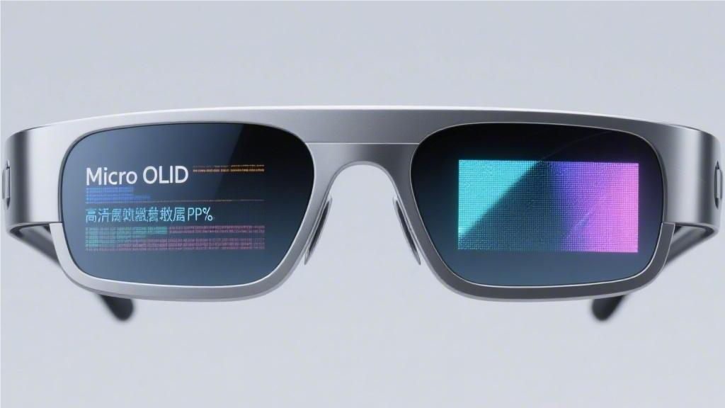
Micro OLED panels are the ideal choice for smart glasses. Their pixel density reaches 3000 to 4000 PPI, presenting high-definition vision without the screen door effect; The weight of a single scre...

Monochrome Micro OLEDs, unblocked by color filters, can reach brightness levels of 100,000 nits and consume only one-tenth the power of full-color versions, making them highly suitable for displayi...
Laisser un commentaire
Ce site est protégé par hCaptcha, et la Politique de confidentialité et les Conditions de service de hCaptcha s’appliquent.