


What is I2C Interface?
I2C uses two bidirectional lines (SCL clock, SDA data) for master-slave communication. With 7/10-bit device addressing, it supports 100kHz (standard) to 3.4MHz (high-speed) modes. Start/stop conditions frame data; devices acknowledge addresses, enabling multi-peripheral links like sensors on wearables.
I2C Definition and Main Uses
A standard I2C bus can support up to 40 components (with 7-bit addressing) and operate over distances of up to 25 feet (approx. 7.6 meters), though practical board-level designs are much shorter. Its initial data rate was a modest 10 Kbps, but modern standard-mode and fast-mode versions operate at 100 Kbps and 400 Kbps respectively, with high-speed modes reaching 3.4 Mbps.
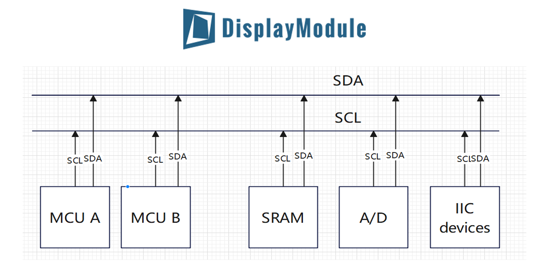
All devices share the same two-wire bus, each with a unique 7-bit address. This setup drastically reduces the number of traces needed on a printed circuit board (PCB), which saves space, lowers complexity, and reduces overall system cost. The bus uses an open-drain design, meaning devices can only pull the signal line low; the high logic level is restored by pull-up resistors connected to a positive voltage supply, typically 3.3V or 5V. The value of these resistors, often between 1 kΩ and 10 kΩ, is a critical design choice that affects the maximum achievable data rate due to the RC time constant of the resistor and the bus capacitance.
The I2C bus is connected to a positive power supply through a pull-up resistor. When the bus is idle, both wires are high. The SDA and SCL of each device are in a "wired-AND" relationship.
It starts a transfer by sending a start condition, then broadcasts the 7-bit address of the target slave device (e.g., a sensor, memory chip, or I/O expander). A single bit following the address specifies if the master wants to write to or read from the slave. The addressed slave responds with a single Acknowledge (ACK) bit, and data transfer proceeds in 8-bit frames.
|
Feature |
I2C |
SPI (Serial Peripheral Interface) |
|---|---|---|
|
Number of Wires |
2 (SDA, SCL) |
4+ (MOSI, MISO, SCLK, SS per slave) |
|
Data Rate |
Standard: 100 kbps, Fast: 400 kbps |
Often >10 Mbps |
|
Addressing |
Software-based (unique addresses on the bus) |
Hardware-based (dedicated Slave Select line per device) |
|
Primary Use Case |
Controlling many low-to-medium speed peripherals |
Streaming data to/from a few high-speed devices |
Common applications include reading from environmental sensors (temperature, humidity), configuring PMIC (Power Management IC) chips, accessing small EEPROM memory, and controlling display drivers. Its two-signal design makes it significantly simpler to route on a PCB compared to SPI, especially when dealing with a high number of connected devices, offering a compelling balance of cost, board space, and adequate performance for a vast range of embedded systems.
Two Wires: SDA and SCL
According to the original specification, a single I2C bus can span up to 25 feet (approximately 7.6 meters) and support communication with up to 40 components at a base data rate of 10 Kbps. Both lines are connected to the positive supply voltage, typically 3.3V or 5V, through pull-up resistors, creating a "wired-AND" configuration where a low signal from any device dominates. The value of these resistors is not arbitrary; it is a critical calculation balancing speed and power, usually falling within the 1 kΩ to 10 kΩ range, with 4.7 kΩ being a common standard value for a 5V bus operating at 100 kHz.
The Serial Data Line (SDA) is the pathway for all actual data transfers. Every byte of information—from a sensor reading to a device address—travels over this single wire. The Serial Clock Line (SCL), generated exclusively by the master device, provides the timing heartbeat for the entire communication. The master pulses the SCL line, and data on the SDA line must be stable during the high periods of the clock pulse. This master-controlled clock is what allows I2C to synchronize devices of different speeds effectively. The electrical state of the bus is defined by this open-drain setup. When no device is pulling a line low, the pull-up resistor brings the voltage to the logical high level. The maximum allowable bus capacitance is a key limiting factor for performance; standard mode specifies a maximum of 400 pF.
A data transfer begins with a START condition, defined as a high-to-low transition of SDA while SCL is high. This unique signal alerts all slaves on the bus to prepare for an address packet. All data bits are transferred on the SDA line after this START condition, with each bit being sampled during a high pulse of the SCL line. The transfer concludes with a STOP condition, a low-to-high transition on SDA while SCL is high. The rise time of the SDA and SCL signals (the time for the voltage to go from a low level to a high level) is a critical parameter. For standard-mode I2C (100 kHz), the maximum rise time is specified as 1000 ns, but for fast-mode (400 kHz), this tightens to 300 ns.
|
I2C Mode |
Clock Speed |
Max. Bus Capacitance |
Max. Rise Time (SDA & SCL) |
Typical Pull-up Resistor (for 5V, 100pF load) |
|---|---|---|---|---|
|
Standard-mode |
100 kHz |
400 pF |
1000 ns |
4.7 kΩ |
|
Fast-mode |
400 kHz |
400 pF |
300 ns |
1.8 kΩ |
|
Fast-mode Plus |
1 MHz |
550 pF |
120 ns |
1.0 kΩ |
In practical design, selecting the correct pull-up resistor (Rp) is a trade-off. The minimum value is determined by the supply voltage (VDD) and the maximum current a device's output driver can sink (typically 3 mA). For a 5V system, the minimum resistor is roughly Rmin = (VDD - Vol) / Iol = (5V - 0.4V) / 0.003A ≈ 1.5 kΩ. The maximum value is constrained by the rise time requirement and the total bus capacitance (Cb). You can estimate it using the formula for an RC circuit: Tr ≈ 0.8473 * Rp * Cb.
Device Addressing on the Same Bus
Each device connected to the I2C bus is assigned a unique 7-bit address, a fundamental parameter set by the manufacturer. This 7-bit address space provides 128 (2^7) possible combinations. However, not all are available for general use; 16 addresses are reserved for special purposes, leaving 112 unique addresses available for standard slave devices. This structure allows a single I2C bus, operating at the standard 10 Kbps rate over a distance of up to 25 feet, to support the theoretical maximum of 40 components mentioned in the original text, as the address space is more than sufficient. The addressing process begins immediately after the master initiates a START condition. The master sends the first byte frame, which consists of the 7-bit slave address followed by a single read/write direction bit, all transmitted over the SDA line in sequence.
The entire address byte is transmitted over a span of 8 clock cycles for the address bits, plus a 9th clock cycle for the acknowledgment. After sending the 7-bit address and the R/W bit, the master releases the SDA line. The slave device whose hardwired address matches the transmitted value then pulls the SDA line low during this 9th clock pulse to send an Acknowledge (ACK). If no device acknowledges, the SDA line remains high, which the master interprets as a Not Acknowledge (NACK), indicating an addressing failure. The probability of an address conflict is a real design consideration. With 112 usable addresses and a bus supporting 40 devices, the chance of randomly selecting components with overlapping addresses is low, but not zero. Many common sensors, like temperature sensors, often share a default address, creating a high probability of conflict if multiple identical devices are used on the same bus. For example, a popular temperature sensor might have a fixed address of 0x48, limiting its use to one unit per bus without additional hardware.
Some devices provide a small number of programmable address pins (e.g., 2 or 3), allowing the designer to set a few bits of the address to a different logic level. Two address pins can create 4 (2^2) unique combinations, and three pins can create 8 (2^3). This effectively multiplies the number of identical devices that can coexist on the same bus. 
Basic Communication Process Steps
The entire communication is synchronized by a clock signal generated by the master device, which can operate at speeds ranging from the original standard of 10 kbps to fast mode's 400 kbps. Each step in this sequence—starting, addressing, reading/writing, and stopping—is defined by specific voltage levels on the SDA and SCL lines relative to each other, with logic high typically at 3.3V or 5V and a low level below 0.8V. The timing between these steps is critical; for a 100 kHz bus, each clock cycle has a period of 10 microseconds, and signals must stabilize within a narrow nanosecond-range window to be read correctly.
Every I2C transaction begins with a START (S) condition, a unique signal that breaks the idle state where both SDA and SCL are high. The master generates this by pulling the SDA line low while the SCL line is still high. This high-to-low transition on SDA acts as a synchronized "attention" signal for all slave devices on the bus. Following the START condition, the master sends the first and most crucial byte of data: the 7-bit slave address plus a 1-bit read/write direction flag. This 8-bit sequence is transmitted over exactly 8 clock pulses, with the data on SDA being required to remain stable for a minimum setup time (e.g., 100 nanoseconds for standard mode) before the rising edge of SCL and must be held until after the SCL line falls. The probability of a collision at this stage is low due to the 112 unique 7-bit addresses available, but it is a key consideration during system design.
The 9th clock pulse is dedicated to the acknowledgment (ACK) cycle. After transmitting the 8 bits of address and direction, the master releases the SDA line, switching its role to a receiver for this single clock cycle. The targeted slave device is responsible for pulling the SDA line low during this high period of the 9th SCL pulse to acknowledge (ACK) that it has received the address and is ready. If the slave fails to pull the line low, a Not Acknowledge (NACK) occurs, indicating an error such as a non-existent address or a busy slave. The data transfer phase then begins. Data is sent in 8-bit bytes, with each byte followed by an ACK/NACK bit from the receiving device. This means for every 8 bits of payload data, there is a 1-bit overhead for acknowledgment, resulting in an 11.1% protocol overhead for the acknowledgment bits alone.
The transaction concludes with a STOP (P) condition, which is a low-to-high transition on the SDA line while the SCL line is high. This signals to all slaves that the bus is being released and they should return to an idle state. The time between a repeated START condition and a STOP condition is variable and depends entirely on the amount of data being transferred. A single command to write one byte to a device's register might take less than 1 millisecond on a 100 kHz bus, while reading a large block of memory could take tens of milliseconds. The master has full control over the clock frequency, and it can even stretch the low period of SCL to pause the transaction if it needs more time to process data, a feature known as clock stretching. This entire sequenced process, from START to STOP, ensures reliable communication with a very low bit error rate under normal operating conditions, making it a robust solution for controlling numerous peripherals with minimal wiring.
Supporting Multiple Controllers
While the typical I2C network operates with a single master, such as an 80C51 microcontroller controlling a set of slave devices, the protocol's design incorporates a sophisticated feature known as multi-master capability. This allows for a system architecture where more than one microcontroller or intelligent controller can share the same two-wire bus. In such a setup, each potential master must possess the logic to not only initiate transmissions but also to detect and respond to the bus state when another master is active. The probability of two masters starting a transmission at the exact same microsecond is low, but over thousands of operational hours, the chance of collision becomes significant. The original I2C specification anticipated this, enabling a bus supporting up to 40 components to include several controllers competing for access, all while maintaining the standard 10 Kbps data rate and 25-foot bus length. The mechanism that prevents data corruption during these access attempts is a non-destructive, electrical bus arbitration process.
The arbitration procedure is a direct consequence of the bus's open-drain design and the wired-AND connection. When the bus is idle (both SDA and SCL high), any master is free to begin a transmission. The critical moment for arbitration occurs when two or more masters generate a START condition within a very narrow time window, roughly on the order of nanoseconds. Each master begins driving the SCL line with its clock signal and starts putting data onto the SDA line, beginning with the 7-bit address of the slave it intends to communicate with.
In a multi-host system, several hosts may simultaneously attempt to initiate the bus to transmit data. To avoid confusion, the IIC bus goes through bus arbitration to determine which host controls the bus.
The clock signal (SCL) is also part of the synchronization process. All masters generate their own internal clock for the transfer. When one master pulls the SCL line low, it resets the clock timing for all other masters on the bus. The result is a synchronized SCL clock whose high period is determined by the master with the longest high period and whose low period is determined by the master with the longest low period. This synchronization ensures that all devices on the bus, including the slaves, see a single, consistent clock signal.
Key Advantages and Limitations
The I2C bus's enduring popularity over several years stems from a clear set of engineering trade-offs that make it ideal for specific applications while limiting its use in others. Its design, which allows connecting up to 40 components with just 2 signal wires over a distance of 25 feet, represents a significant saving in board space and interconnect complexity. The protocol's original 10 Kbps speed has been expanded to over 3.4 Mbps in modern implementations, but its fundamental characteristics create a distinct profile of strengths and weaknesses. The choice to use I2C over alternatives like SPI or UART often boils down to a direct calculation involving the number of components, required data bandwidth, and the cost and space constraints of the printed circuit board (PCB). A system with 10 sensors might see a 60-80% reduction in necessary GPIO pins on the host microcontroller by using I2C compared to a parallel or individual UART approach.
Key Advantages:
-
Minimal Pin Count and Board Space: This is the most significant advantage. With only 2 bidirectional lines (SDA and SCL), I2C drastically reduces the number of traces on a PCB. This saves space, simplifies routing, and lowers the layer count of the board, which directly reduces manufacturing costs. A microcontroller needing to communicate with 20 different chips would require 40+ pins for a parallel bus or individual chip selects, but only 2 pins with I2C, a 95% reduction in pin usage.
-
Hardware Simplicity and Cost-Efficiency: The open-drain hardware requires only two pull-up resistors per bus, regardless of the number of devices (up to the 400 pF capacitance limit). The component count is very low, and the interface is integrated into thousands of low-cost peripheral chips like sensors, EEPROMs, and I/O expanders, keeping the total system cost down.
-
Built-in Multi-Master Support and Arbitration: Unlike simpler serial protocols, I2C natively supports a multi-controller system. The bus arbitration and clock synchronization processes are handled in hardware, requiring no additional software overhead or extra control lines. This allows for robust, redundant system designs where multiple microprocessors (like two 80C51s) can share the bus without data corruption, resolving conflicts typically within 1 microsecond.
-
Flexible Data Rates and Device Compatibility: The clock stretching feature allows slower slaves to throttle the data rate from a faster master, ensuring compatibility between devices of different speeds on the same bus. This simplifies the integration of a low-speed, low-power sensor operating at 100 kHz with a main controller running the bus at 400 kHz.
Key Limitations:
-
Lower Data Throughput: The half-duplex nature (data travels in one direction at a time) and the overhead of 7-bit addressing plus ACK bits create inherent speed limitations. Even at 400 kHz, the effective data rate is lower due to protocol overhead. It is unsuitable for high-speed tasks like driving displays or streaming audio, where SPI with speeds often exceeding 10 MHz is a better choice.
-
Software Complexity and Debugging Difficulty: The protocol is entirely controller-driven, placing the burden of generating precise timing and handling all states (START, STOP, ACK, NACK) on the software driver. This can result in more complex code than for a simpler UART. Debugging communication issues, such as a missing ACK from a slave at address 0x68, can be challenging without a logic analyzer to view the exact signal timing on the 3.3V SDA and SCL lines.
-
Susceptibility to Noise and Signal Integrity: The bus's high impedance when pulled up makes it more vulnerable to electrical noise, especially over longer distances approaching the 25-foot maximum. The total bus capacitance is a hard limit; exceeding approximately 400 pF can cause signal rise times to degrade, leading to communication errors. Careful selection of pull-up resistor values (e.g., 4.7 kΩ for 100 kHz) is critical for reliable operation.
-
Limited Address Space and Potential for Conflicts: The 7-bit address space provides only 112 unique addresses for general use. With the proliferation of I2C devices, address conflicts are common. Using two identical temperature sensors with a fixed address of 0x48 on the same bus is impossible without an external multiplexer, adding cost and complexity. The 10-bit addressing extension exists but is not universally supported.
The main advantage of the I2C bus is its simplicity and efficiency. Because the interface is directly on top of the component, the I2C bus takes up very little space, reducing board space and the number of chip pins, reducing interconnection costs.
I2C offers an excellent cost-to-performance ratio for applications involving multiple low-to-medium speed control and sensing devices within a compact system. Its advantages are most pronounced when the number of devices is high, the data rate requirement is below 1 Mbps, and system cost is a primary driver.
En lire plus
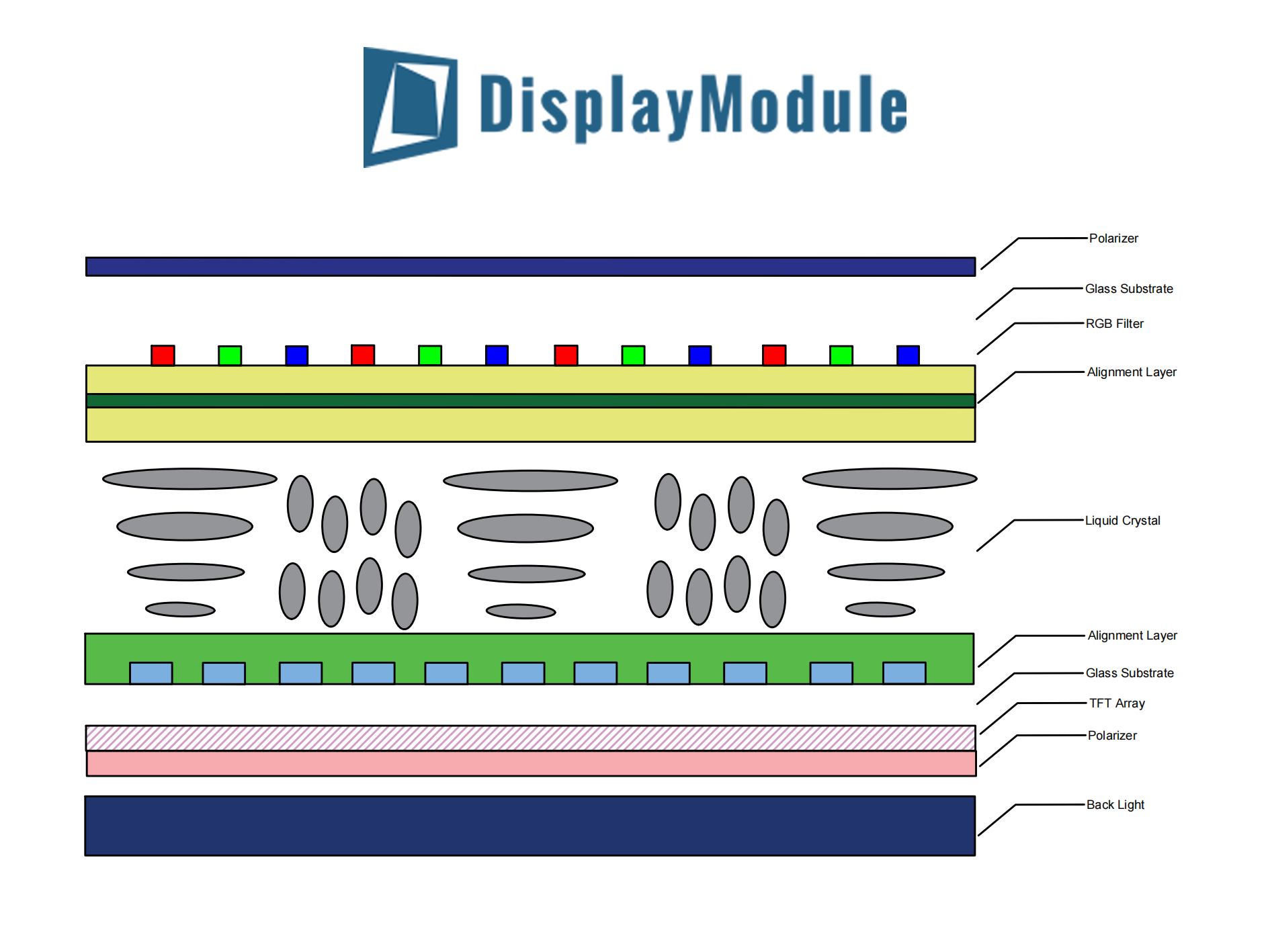
TFT structures comprise a glass substrate, gate electrode (Mo, 100–200nm thick), SiO₂ insulator (≈300nm), semiconductor layer (a-Si, 50–100nm), and source/drain metals (150–200nm). Gate volta...
From: Author Clock: A Novel Way To Tell Time Do have the same experience as me? Sometimes I am inspired by quotes from books or movies. Those quotes inspire me to read books or watch movies. R...
Laisser un commentaire
Ce site est protégé par hCaptcha, et la Politique de confidentialité et les Conditions de service de hCaptcha s’appliquent.