


What is SPI (Serial Peripheral Interface) Bus?
SPI, a synchronous serial bus by Motorola, uses 4 lines: SCLK (clock), MOSI (master-out), MISO (master-in), and SS (slave-select). Master drives SCLK for full-duplex, 8/16-bit transfers up to tens of Mbps; pulling SS low selects a slave for communication.
SPI Basic Definition and Purpose
A typical SPI implementation uses only four wires, a significant pin-saving advantage on a chip's package compared to the parallel buses of the past, which could require 8, 16, or more pinsfor data alone. This efficiency in physical connections simplifies Printed Circuit Board (PCB) layout and reduces overall system cost. Today, it's integrated into virtually every modern microcontroller, such as STM32 series, where it can achieve clock speeds often exceeding 10 MHz, and in some cases reaching up to 42 MHzor even 100+ MHzin high-speed versions, enabling data transfer rates that are essential for time-sensitive applications.
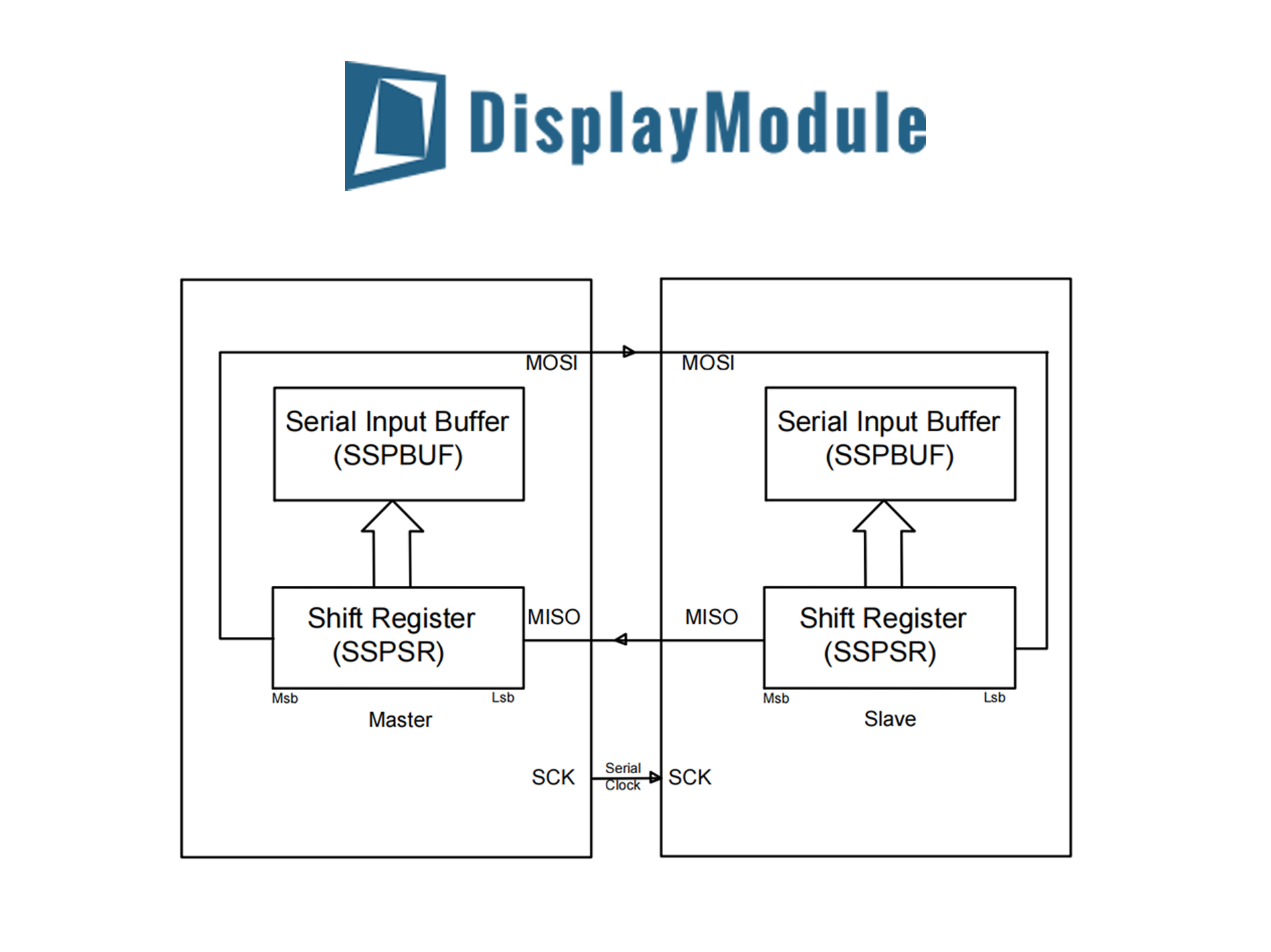
At its heart, SPI is a simple shift-register-based protocol. The bus consists of four essential signals: MOSI (Master Out Slave In), MISO (Master In Slave Out), SCLK (Serial Clock), and SS/CS (Slave Select). The master device controls the communication by generating the clock signal on SCLK. For every clock pulse generated by the master, a single bit is shifted out from the master to the slave on the MOSI line, and simultaneously, a single bit is shifted from the slave back to the master on the MISO line. This full-duplex operation means that an 8-bitdata transfer results in 8 bitsbeing sent and 8 bitsbeing received in the same 8 clock cycles, making it highly efficient for many register-based read/write operations.
|
SPI Mode |
CPOL |
CPHA |
Clock Idle State |
Data Sampling Edge |
|---|---|---|---|---|
|
0 |
0 |
0 |
Low (0) |
Rising (1st edge) |
|
1 |
0 |
1 |
Low (0) |
Falling (2nd edge) |
|
2 |
1 |
0 |
High (1) |
Falling (1st edge) |
|
3 |
1 |
1 |
High (1) |
Rising (2nd edge) |
Practical Consideration:You must always consult the slave device's datasheet to determine the correct SPI mode. For example, a common temperature sensor like the MAX31855specifies operation in SPI Mode 1 (CPOL=0, CPHA=1). Configuring the master for the wrong mode, even with the correct clock speed, will result in reading garbage data.
The master pulls this line low (0V)to select a particular slave device before initiating a clock signal. This is the primary method for connecting multiple slaves to a single SPI master. A system with threeslave devices would require threeseparate SS/CS lines from the master, sharing the single MOSI, MISO, and SCLK lines. The high speed of SPI is a direct result of this hardware-based addressing and lack of a complex packet structure. There is no need to send device addresses or other protocol overhead bits within the data stream, unlike in I2C communication. This allows the bus to operate at its maximum clock frequency, with the data transfer rate being a direct function of that frequency. For a 16 MHzclock, the effective data rate can be close to 16 Mbps, minus negligible software delays.
Connecting the Four Essential Wires
The connection is essentially a point-to-point link between a single master device, like an STM32 microcontroller, and one or more slave devices, such as a 25LC1024 EEPROMmemory chip.
The maximum practical distance for a standard SPI connection is typically less than 1 meter, and often kept to just a few centimeters on a PCB, as the high-speed signals are susceptible to noise and degradation over longer wires. The clock speed, which can range from a few kHzfor low-power sensors to over 50 MHzfor high-speed memories, is entirely controlled by the master and must be configured to not exceed the slave device's maximum specified frequency, often found in the "AC Electrical Characteristics" table of its datasheet.
The first wire, Serial Clock (SCLK/SCK), is generated exclusively by the master device. Its sole purpose is to provide the timing heartbeat for all data movement. There is no fixed speed; the master's microcontroller peripheral can typically be programmed to output a clock derived from its system clock with a wide range of division factors, for example, generating a 10 MHz SCLKfrom a 80 MHz system clockby using a divider of 8. The other three wires are for data and control. The Master Out Slave In (MOSI)line is a one-way street for data flowing from the master to the currently selected slave. Simultaneously, the Master In Slave Out (MISO)line carries data from the selected slave back to the master. This dual data path enables true full-duplex communication, meaning that for every 8 clock cycles, 8 bitsare transmitted and 8 bitsare received at the same time.
The fourth wire, Slave Select (SS), also known as Chip Select (CS), is the control line that activates a specific slave device on the bus. This pin is active-low, meaning the slave device is enabled when the signal is at a logic low voltage (e.g., 0V). In a system with only one slave, the slave's SS pin can be permanently tied to ground, but this is often not recommended for production systems as it removes the master's ability to reset the slave by toggling the SS pin. In a multi-slave setup, the master must have one dedicated SS pin for each slave device. For example, to connect three SPI slaves, the master needs three separate SS lines, while the SCLK, MOSI, and MISO lines are shared among all slaves in a parallel bus configuration.
The master selects a slave by pulling its corresponding SS line low; it must ensure that only one SS line is active at any given time to prevent bus contention on the MISO line. The timing of the SS signal is also critical. The SS line must be pulled low for the entire duration of the data transfer, which could be 8 clock cyclesfor a single byte or 128 cyclesfor a 16-bytedata buffer write. De-asserting SS too early is a frequent cause of corrupted data packets. When dealing with devices from different logic families, such as a 3.3V masterand a 5V slave, a level-shifting circuit must be inserted into all four signal paths to prevent damage and ensure logical high and low voltage thresholdsare met reliably.
Master-Slave Communication Process
Unlike asynchronous protocols like UART that require pre-agreed baud rates, SPI leverages the master-generated clock to achieve precise timing, enabling reliable data transfer at high speeds, often ranging from 100 kHzto over 50 MHzdepending on the microcontroller and slave device capabilities. The entire process is built on a simple shift-register mechanism: both the master and the slave contain an internal 8-bitor 16-bitshift register. When the master initiates a transfer, these registers are effectively linked via the MOSI and MISO lines to form a distributed, circular 16-bit(for 8-bit data) or 32-bit(for 16-bit data) shift register.
The process begins with the master asserting the Slave Select (SS) line for the target device, pulling it from a logic high (3.3Vor 5V) down to a logic low (0V). This activation must meet a minimum setup time, often in the range of 10 to 100 nanoseconds, before the first clock edge appears.
After the 8th clock cycle, the entire byte has been exchanged. The master then has a critical decision to make. If it needs to send or receive more data, it can continue toggling the clock for another 8 cyclesto transfer a second byte, perhaps as part of a 16-bitcommand or a multi-byte buffer read. The SS line must remain active low for the entire duration of a multi-byte transaction. Once the transfer is complete, the master de-asserts the SS line, driving it back to a logic high. This action typically signals the end of a command frame to the slave.
A common practical example is reading from a SPI-based accelerometerlike the ADXL345. The master might need to send a single 8-bitregister address byte (e.g., 0x80 | 0x32to read the X-axis data starting at register 0x32) and then immediately execute a second 8-bittransfer. During this second transfer, the master sends a dummy byte (e.g., 0x00) while the slave shifts out the requested data. This highlights the full-duplex natureof SPI; even when the intent is only to read, the master must generate clock cycles by sending data to receive data. The total transaction time for a 2-byte read like this, at a 10 MHzclock speed, is just (8 bits + 8 bits) / 10 MHz = 1.6 microseconds, demonstrating the protocol's high speed.
The Role of Chip Select (CS)
In a system with multiple peripherals—for instance, a 3.3Vmicrocontroller connected to a SPI Flashchip, a digital sensor, and an ADC—the CS pin is the master's tool for eliminating signal conflict on the shared data lines. This active-low signal, typically held at a logic high voltage (e.g., 3.3V)when inactive, is pulled to a logic low voltage (0V)by the master to initiate a communication session with a specific slave. The simplicity of this hardware addressing is a key differentiator from protocols like I2C; it removes the need for embedded 7-bit or 10-bit device addresseswithin the data stream, thereby increasing effective bandwidth. For a master to manage Nnumber of slaves, it must dedicate Nseparate GPIO pins exclusively for CS functions. This means a system with fiveSPI slaves requires fiveCS lines, but the total pin count on the master remains at 3 + N(SCLK, MOSI, MISO + N CS), which is often more efficient than parallel buses for a small number of devices. The timing of the CS signal is critical; datasheets specify a minimum setup time, often 10 to 50 nanoseconds, that the CS line must be asserted low before the first clock edge, and a similar hold time after the last clock edge, to ensure reliable synchronization.
The CS pin serves three critical hardware and protocol-management functions that are essential for reliable system operation.
-
Slave Activation and Deactivation:The primary role of the CS signal is to activate a specific slave device's output drivers. When CS is high (inactive), the slave's MISO pin must be in a high-impedance (high-Z) state, effectively disconnecting it from the bus.
-
Framing Data Transactions:The CS signal defines the boundaries of a complete data transaction. A single transition from high to low and back to high often frames a command and its response. For example, communicating with a SPI EEPROM like the 25LC512involves pulling CS low, sending a 8-bitinstruction code (e.g.,
0x03for a read), followed by a 24-bitmemory address, and then clocking out a sequence of data bytes. The entire read operation, which might transfer 16, 32, or even 256 bytes, is contained within a single continuous CS low pulse. -
Slave Reset and Synchronization:A less obvious but vital function is resetting the slave's internal state machine. Many slave devices, such as RF transceiversor accelerometers, require a specific sequence of commands. Toggling the CS line (pulling it high for a minimum period, often 100 ns, and then low again) provides a reliable hardware reset that clears the slave's internal logic and ensures the master and slave are synchronized for a new command sequence.
The master loses the ability to reset the slave via hardware. Furthermore, during the microcontroller's power-on resetphase, which may last for several milliseconds, its I/O pins can be in an undefined state, causing the slave to receive garbled clock and data signals. This can put the slave into an unexpected state, requiring a full power cycleto recover. For reliable operation, the master should always control the CS line, even for a single slave. The voltage level of the CS signal is also critical; a master operating at 1.8Vmust ensure its GPIO can meet the high-level input voltage threshold (VIH)of a 3.3Vslave, which may require a level shifter if the threshold is above ~2.0V. Proper management of the CS line, with attention to timing specifications and voltage levels, is a >90% factorin achieving stable SPI communication.
Connecting Multiple SPI Devices
A standard microcontroller like an STM32F103may have twoor threededicated SPI peripherals, but a system might need to connect to five or moresensors and memory chips. The fundamental challenge is managing the shared MISO line to prevent bus contention, a state where multiple slaves try to drive the line to different logic levels simultaneously, which can increase current consumption by tens of milliampsand cause signal integrity issues. There are three primary methods to scale an SPI network, each with distinct cost and performance implications. The most straightforward approach is the parallel busmethod, which uses dedicated Chip Select (CS) lines for each slave. For a system with Nslaves, this method requires 3 + Npins on the master (SCLK, MOSI, MISO + N CS pins). A second method, daisy-chaining, uses only fourpins total but requires all slaves to support this feature
-
Standard Parallel Bus with Individual Chip Selects:This is the most reliable and widely used method. Each slave shares the global SCLK, MOSI, and MISO lines. The master has a unique GPIO pin connected to each slave's CS pin. To communicate with a specific device, the master pulls only that slave's CS line to 0V, while keeping all others at a logic high (e.g., 3.3V). This ensures that only the selected slave's MISO output is active, while the others remain in a high-impedance state. The key advantage is maximum speed; each slave can be operated at its highest rated clock frequency, up to 50 MHzor more. The drawback is the linear increase in GPIO usage. Connecting 8 slavesrequires 11 GPIO pinson the master. The PCB layout can become congested, as the 3 main signal linesmust be routed to every chip, which can increase trace length and susceptibility to noise if the total path length exceeds roughly 30-50 cm.
-
Daisy-Chain Configuration:Some SPI devices, particularly a series of shift registers like the 74HC595or certain digital potentiometers, support a daisy-chain configuration. In this setup, the MISO of the first slave is connected to the MOSI of the second slave, and so on. The master uses a single CS linefor the entire chain. Data sent by the master shifts through the first slave's register and then into the second slave's register over multiple clock cycles. For a chain of three8-bitshift registers, the master must send 24 bitsof data to update the last slave in the chain.
-
Using an External Demultiplexer (Demux):When a design is pin-constrained and daisy-chaining isn't feasible, an external digital demultiplexer can be used. A 3-to-8 demuxchip (e.g., 74HC138), costing under $0.10, uses 3 control pinsfrom the master to select 1 of 8 output lines. Each output line acts as a CS signal for a slave. This reduces the pin count from Nto log2(N), rounded up. For 8 slaves, the pin count is only 3 (for the demux) + 3 (SPI) = 6 pins, a 37.5% reductioncompared to the 11 pinsrequired for the standard method. The trade-off is increased software complexity, as the master must set the demux's address lines before each transfer, adding a microsecond-scaledelay. Furthermore, all slaves on the demux must operate at the same SPI mode and a clock speed suitable for the slowest device on the bus, which could limit performance if a 100 kHzsensor is mixed with a 20 MHzmemory chip. For mixed-voltage systems, such as a 1.8Vmaster controlling 3.3Vslaves, a level-translating demux or buffer like the 74LVC1T45must be used, adding a few more components and milliwattsof power consumption.
Pros and Cons of Using SPI
The Serial Peripheral Interface (SPI) offers a compelling set of advantages for embedded systems, but its limitations make it unsuitable for certain applications. The following table provides a high-level summary of its core strengths and weaknesses against other common protocols like I2C and UART.
|
Protocol |
Max Speed (Typical) |
Pins (Master + 1 Slave) |
Hardware Complexity |
Error Checking |
|---|---|---|---|---|
|
SPI |
10 - 50+ MHz |
4 |
Low |
None |
|
I2C |
100 kHz - 3.4 MHz |
2 |
Medium |
ACK/NACK Bit |
|
UART |
9.6 - 115.2 kbps |
2 |
Low (Async) |
Optional Parity |
A read operation from a SPI Flash memoryat a 50 MHzclock speed can achieve a data rate of nearly 50 Mbps, which is over 400 times fasterthan a standard I2C read at 100 kHz. This speed is essential for applications like driving high-resolution displays, streaming data from fast ADCs, or executing code directly from external memory (XIP). Furthermore, SPI's hardware simplicityreduces CPU load. The slave device relies entirely on the master's clock, eliminating the need for a precise internal oscillator and the associated 2-5% baud rate errortolerance required by UARTs. Data transfers are not confined to 8-bitbytes; they can be any length—12 bitsfrom an ADC or a 20-bitcommand to a DAC—providing extreme flexibility. The simple hardware addressing via the Chip Select (CS) line is more efficient for point-to-point links than I2C's 7-bit or 10-bitaddressing scheme, which consumes a portion of each data packet.
The primary limitation is the lack of a hardware acknowledgment mechanism. Unlike I2C, where a slave sends an ACK bit after each byte, the SPI master has no way of knowing if a slave has received data or is even present on the bus. If a master tries to read from a disconnected slave, it will simply receive garbage data without any error indication, leading to a potential 100% silent failure ratein that communication path. This necessitates robust software routines to validate all data transactions. Secondly, SPI's pin count scales linearly with the number of slaves. While I2C maintains a constant 2-wirebus regardless of device count, connecting NSPI slaves requires 3 + Nwires (SCLK, MOSI, MISO, and N CS lines). For a system containing 8 slaves, this consumes 11 GPIO pinson the master, compared to only 2 pinsfor an I2C bus, significantly increasing the BOM cost and PCB complexity for larger networks.
The probability of an undetected error can be 1-5%in harsh industrial environments, making pure SPI unsuitable for safety-critical applications without a robust software-based checksum layer. Finally, SPI is designed for short-distance, on-PCB communication. The high-speed signals are susceptible to capacitance, resistance, and electromagnetic interference, limiting reliable operation to distances typically less than 1 meter, and often to just 10-30 centimeters. In contrast, RS-485 (a standard for UART) can reliably transmit data over 1200 meters.
En lire plus

From: Author Clock: A Novel Way To Tell Time Do have the same experience as me? Sometimes I am inspired by quotes from books or movies. Those quotes inspire me to read books or watch movies. R...

Organic Light Emitting Diodes (OLEDs) are a type of technology that is taking the display and lighting industry by storm. They are increasingly being used in the latest smartphones, televisions, l...
Laisser un commentaire
Ce site est protégé par hCaptcha, et la Politique de confidentialité et les Conditions de service de hCaptcha s’appliquent.