



What is the difference between mini OLED and OLED
The difference is one of scale and backplane, not of chemistry. Both devices light organic emitters with a current, so both switch off to true black, but a panel sold as mini OLED is built on a much finer pixel grid with a different driving substrate. That finer grid is what buys the high pixel density small products need, and it is also what makes the panel harder to make.
A name that needs checking
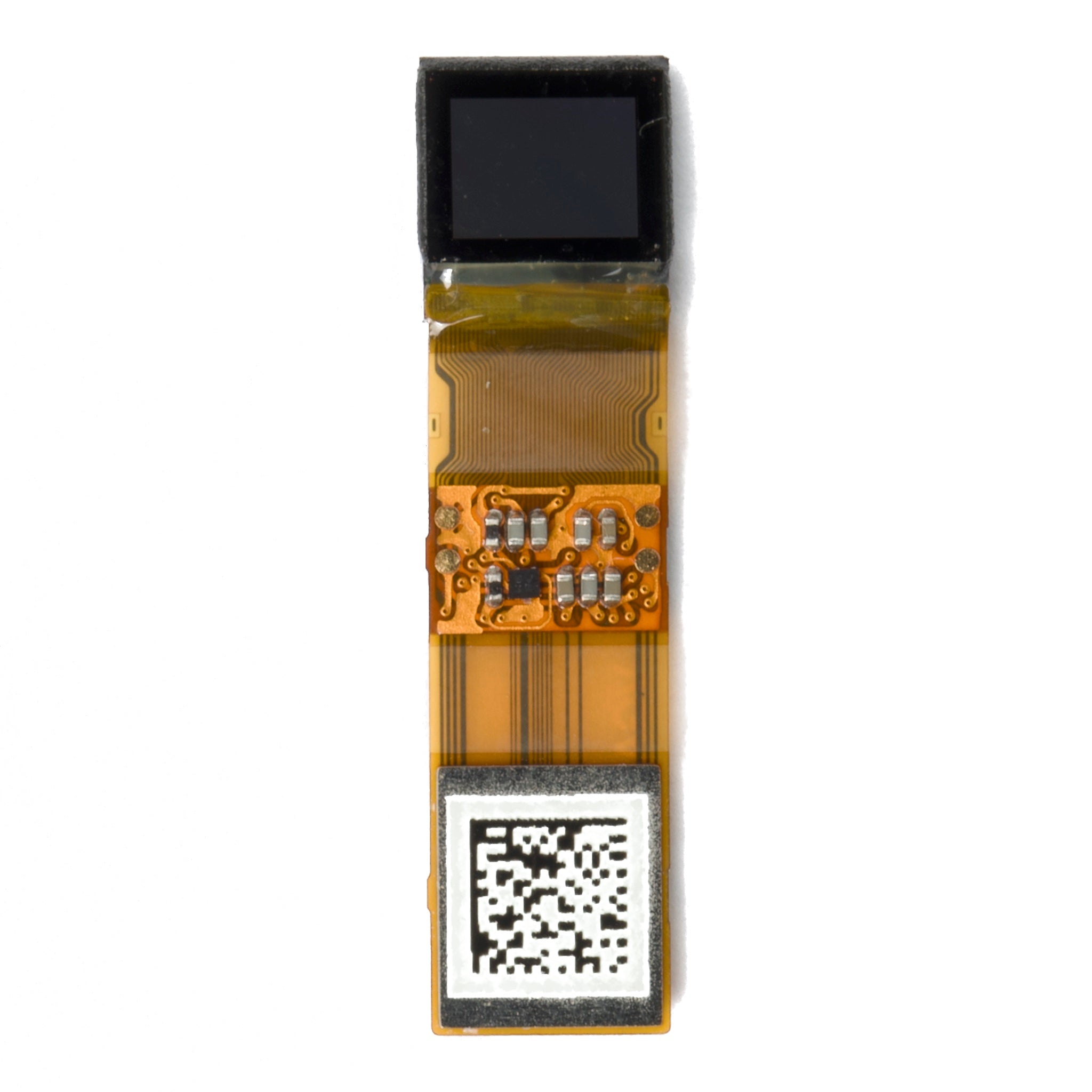
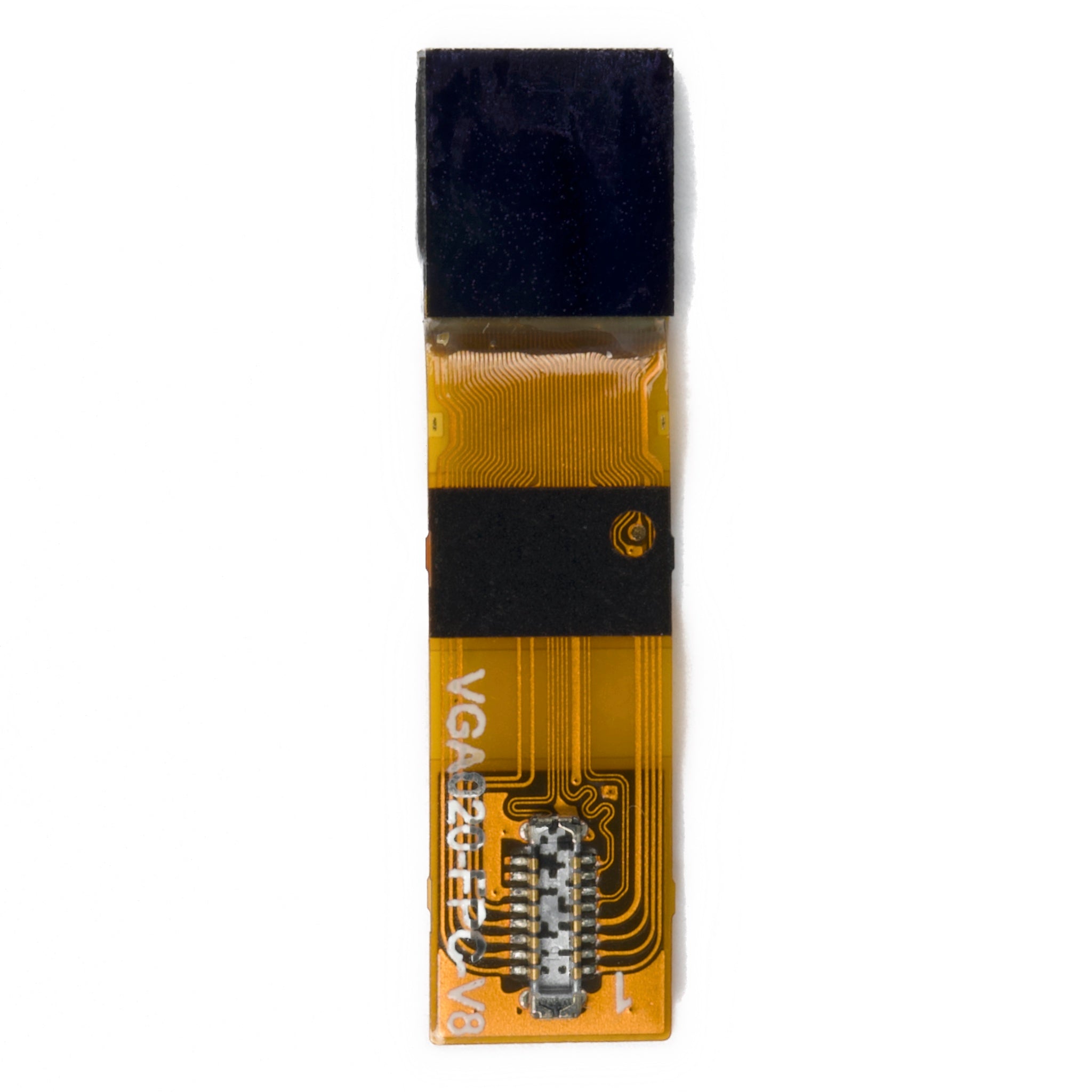
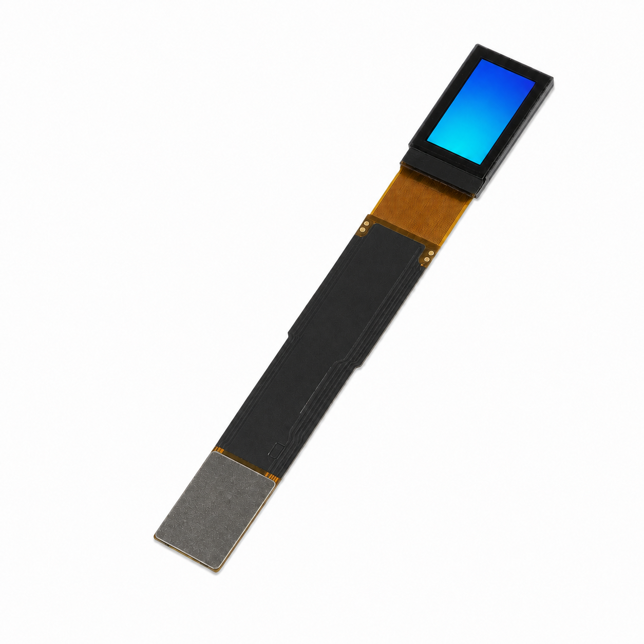
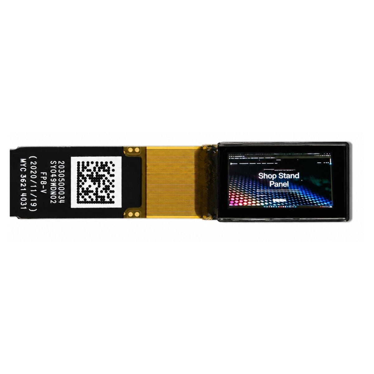
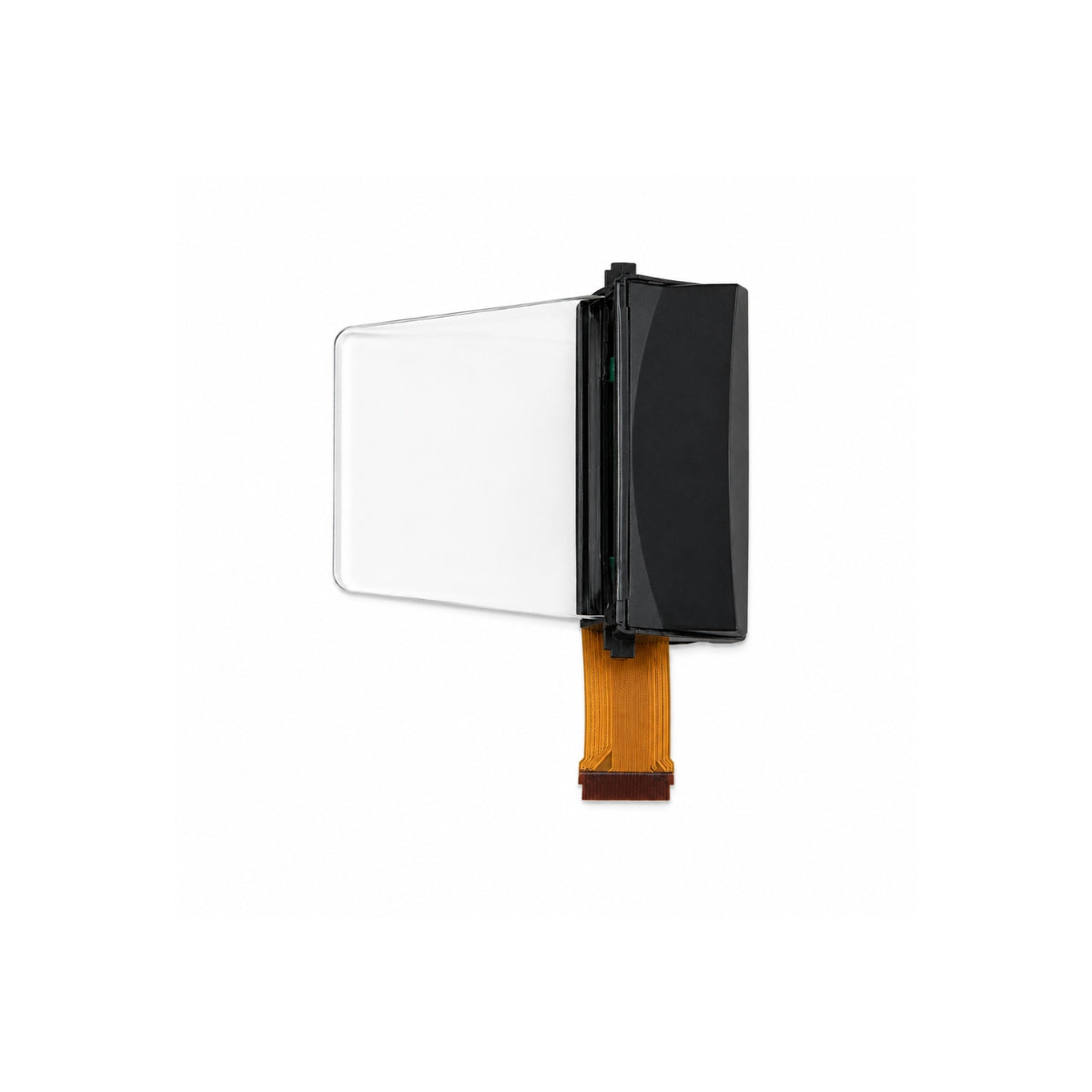
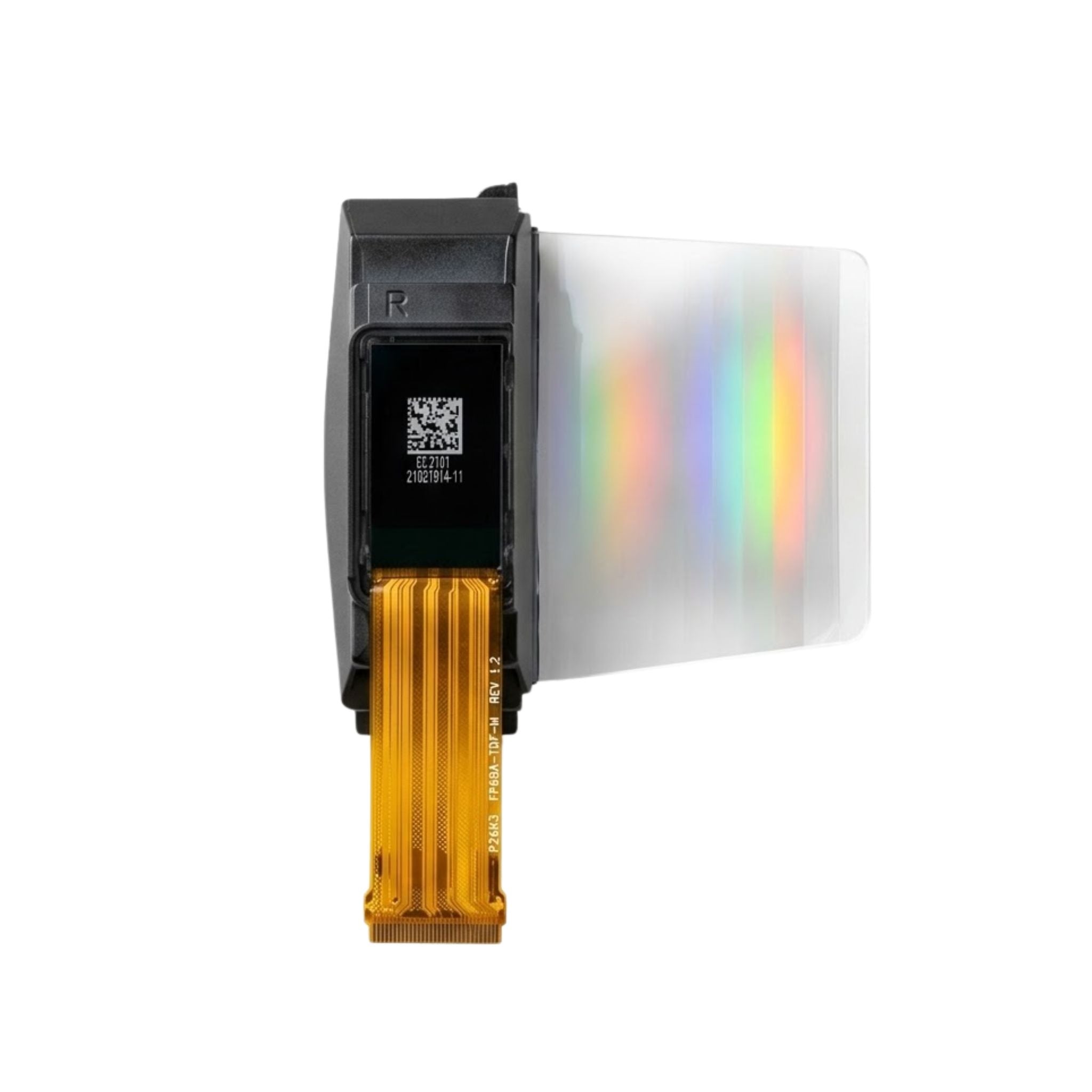
Mini OLED is not a term fixed by a standards body, and it is used for at least three different things. It can mean a small OLED microdisplay, often built on a silicon backplane and used in camera viewfinders and near-eye optics. It can mean a compact glass or plastic OLED panel in a watch or a wearable. It is also used, incorrectly, for mini-LED, which is a backlight made of many small LEDs behind an LCD and has nothing to do with organic emitters.
That ambiguity matters when you read a datasheet. Before comparing anything, ask for the emitter stack, the backplane material and the pixel pitch. Those three answers place the part in the right family and make the rest of the numbers comparable.
What the two families share
An organic light-emitting diode is a stack of thin organic layers between two electrodes. Current through the stack recombines carriers and light comes out, so each pixel is its own light source and needs no backlight or liquid crystal shutter. Flat-panel displays divide into emissive and light-modulating types, and OLED sits in the emissive group alongside plasma and inorganic LEDs, while LCD belongs to the modulating group.[2]
Because the pixel is the light source, black is produced by driving the pixel off rather than by blocking a lamp. In a lit room the black level is then limited by reflection from the cathode and the metal lines, which is why a circular polariser or an anti-reflective layer is part of the optical design rather than an accessory.
Pixel pitch sets the density
Pixel density is limited by how small a pixel and its driving circuit can be patterned. On a glass backplane with low-temperature polysilicon or an oxide semiconductor, the pitch is measured in tens of micrometres, which lands at several hundred pixels per inch on a phone-sized panel. On a crystalline silicon backplane, the driving circuit is made with integrated-circuit lithography, so the pitch falls to a few micrometres and the density rises into the thousands of pixels per inch on a panel smaller than a postage stamp.
That is the real dividing line. A miniature OLED for a watch may be small but still sit in the hundreds of pixels per inch, while an OLED microdisplay for a viewfinder is both small and extremely dense. Size alone does not tell you which one you have.

How brightness is quoted
Luminance figures for emissive panels are conditional, and the conditions are usually left out of the headline. A number measured on a small white window can be much higher than what the panel holds with the whole screen white, because drive current and heat are shared across all pixels and many drivers limit average power. Duration matters as well: a peak that holds for a few seconds is not a sustained figure.
For a fair comparison, ask for luminance at a stated average picture level, at a stated white point, after warm-up, and with the dimming or power-limiting behaviour described. The same caution applies to colour: gamut measured on a small patch will not match gamut measured across the full field.
Lifetime and burn-in
Organic emitters fade, and they fade at different rates for different colours, with blue usually the fastest. Lifetime is therefore quoted as the time to a stated proportion of initial luminance, at a stated initial luminance, temperature and drive duty. A figure without those conditions cannot be compared with another supplier's figure.
Differential ageing is what users see as burn-in: a static bright element such as a status bar ages its pixels faster than the surrounding area, and the pattern becomes visible later. Compensation circuits that track and correct pixel usage help, but the design of the user interface does as much work as the electronics. Products that show one fixed layout for hours at high brightness are the hardest case for any emissive panel.
Colour, filters and conversion
There are three common ways to get colour. White emitters with red, green and blue colour filters are simple to pattern but throw away a large share of the emitted light in the filters. Directly patterned red, green and blue emitters avoid that loss but are harder to mask at fine pitch. Quantum-dot colour conversion sits between the two, using a blue emitter and converting part of the output, which can widen the gamut while keeping the emitter stack simpler.
Which route a mini panel uses changes its efficiency, its gamut and its lifetime, and it is one of the first things to establish when a supplier quotes a colour gamut figure.
Encapsulation and substrate
Organic layers react with water and oxygen, so every OLED is sealed. Thin-film encapsulation alternates inorganic and organic layers to slow permeation, and the specification that matters is the water-vapour transmission rate the seal is designed and tested for, not the number of layers. Flexible parts add a polymer substrate in place of glass, which saves thickness and allows a curve, but demands a lower permeation rate because the plastic itself is not a barrier.
Small panels are often the first place a tighter seal appears, because a short edge length leaves less room for edge ingress and because the product is expected to run for years in a watch or a headset.
Choosing between them
The choice follows the product, not the label on the datasheet.
| Requirement | Favours | Reason |
|---|---|---|
| Highest pixel density in a tiny area | Silicon-backplane OLED microdisplay | Integrated-circuit lithography allows a pitch of a few micrometres |
| Thin, curved or lightweight wearable | Small OLED on a polymer substrate | No backlight stack, and the substrate can be thin |
| Large diagonal at moderate cost | Conventional OLED or LCD | Mother-glass economics and mature supply |
| Long static display in sunlight | LCD, or a reflective technology | No emitter ageing and higher sustained output |
| Deep black in a dim room | Either OLED family | The pixel switches off instead of blocking a lamp |
Questions for a supplier
Ask which backplane the part uses and what the pixel pitch is. Ask for luminance at a defined average picture level, with the power-limiting behaviour stated. Ask for lifetime at a stated initial luminance and temperature, and for the blue sub-pixel figure separately. Ask what the seal is qualified to, whether the part is glass or polymer, and how the driver compensates for ageing. Ask for the measurement conditions behind the contrast and colour numbers, since ISO 9241-307 sets out how those measurements are made and reported.[1]
If the answers are clear, the family name stops mattering: you can compare a dense microdisplay against a conventional panel on the terms that decide the design. If the answers are vague, the datasheet is marketing. For products that end up on a glass panel with a backlight, the OLED modules and micro OLED modules ranges show how the two formats are specified in practice.
Summing up
Mini OLED and OLED are the same device at different scales. The smaller part wins on pixel density because its backplane is patterned more finely, and it pays for that with tighter sealing, harder colour patterning and a shorter path to ageing effects. Compare them by pitch, backplane, luminance conditions and lifetime basis, not by the adjective.
References
- ISO 9241-307:2008 — Ergonomics of human-system interaction — Part 307: Analysis and compliance test methods for electronic visual displays. International Organization for Standardization. https://www.iso.org/standard/40102.html
- Hilsum, C. (2010). Flat-panel electronic displays: a triumph of physics, chemistry and engineering. Philosophical Transactions of the Royal Society A, 368(1914), 1027–1082. https://doi.org/10.1098/rsta.2009.0247
En lire plus
Micro OLED displays are typically produced by depositing organic light-emitting materials onto a small silicon or glass substrate (0.5–1.3 inches) using.
A Micro LED display is a self-emissive, inorganic technology where each tiny light-emitting diode (LED) acts as an individual pixel , enabling vibrant.
Laisser un commentaire
Ce site est protégé par hCaptcha, et la Politique de confidentialité et les Conditions de service de hCaptcha s’appliquent.