


Custom TFT Display Modules A Buyer's Guide | Specifications, Interfaces
Selecting a TFT module must closely align with specifications and interfaces. Resolution (e.g., 800x480) and brightness (starting at 500 nits) are fundamental; industrial scenarios require attention to wide temperature ranges (e.g., -20℃~70℃).
Interface determines the performance ceiling: RGB/MCU interfaces offer cost advantages, suitable for static images; MIPI interface has high speeds (often exceeding 1Gbps), making it the preferred choice for video streams.
Specifications
When selecting a custom TFT display module, its specification parameters are the objective quantification of its function and performance.
Parameters include size (e.g., 7.0 inches), resolution (e.g., 800x480 pixels), brightness (500 nits suitable for indoor use), and interface type (e.g., MIPI-DSI).
These indicators collectively determine image clarity, power consumption, environmental adaptability (operating temperature -20℃ to 70℃), and system compatibility.
They are the direct basis for evaluating whether the display solution meets the requirements of industrial, medical, or consumer electronics applications.
Display Parameters
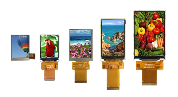
How to match screen size and clarity?
Physical size is measured by the diagonal length, but the precise dimensions of the actual active display area (e.g., 154.08mm × 85.92mm) are more critical for mechanical design.
Resolution and size together determine the pixel density (PPI).
High PPI provides a finer visual experience but also significantly increases the system load: driving a 10.1-inch 1280×800 screen requires over 2.5 times the data volume compared to a 5-inch 800×480 screen, placing higher demands on processor performance and memory bandwidth.
Different application scenarios have de facto resolution standards:
-
3.5-inch screens commonly use 320×240 (QVGA)
-
5.0-inch screens correspond to 800×480 (WVGA)
-
7.0-inch screens often use 1024×600 (WSVGA)
-
10.1-inch screens typically match 1280×800 (WXGA)
Brightness and Ambient Light Conditions
In a bright office with an illuminance of about 500 lux, a screen brightness of at least 300 nits is required for comfortable reading.
In outdoor direct sunlight environments (illuminance exceeding 10,000 lux), brightness requirements may exceed 1000 nits, and need to be paired with polarizers and low-reflection glass.
The brightness uniformity of industrial display modules is typically required to be above 80% (meaning the brightness of any area of the screen is not less than 80% of the center brightness), avoiding noticeable light and dark differences.
Impact of Contrast Ratio on Image Gradation
A static contrast ratio of 800:1 means the brightness difference between the whitest and blackest is 800 times, resulting in sharper text edges and richer image gradation.
It is important to note that some advertised high dynamic contrast ratios (e.g., 1,000,000:1) are achieved by dynamically adjusting the backlight, which is a different measurement standard from static contrast ratio.
Viewing Angle Depends on Panel Technology
Viewing angle parameters are determined by the liquid crystal alignment.
TN panels may exhibit significant color shift and contrast reduction at just 30 degrees off-center, while IPS/FFS technology, by horizontally rotating the liquid crystal molecules, achieves an ultra-wide viewing angle of 178 degrees, maintaining color accuracy and contrast consistency from almost any viewing direction.
The widespread adoption of IPS technology in medical diagnostic displays and automotive center consoles is based on this characteristic.
Actual Performance of Color Depth
Color depth determines the smoothness of color transitions.
6-bit panels simulate 16.7M colors through FRC (Frame Rate Control) dithering, but color banding may be observed when displaying gradient colors.
True 8-bit panels (16.7M colors) can achieve smooth 256-level grayscale transitions. Professional graphic displays require 10-bit (1.07 billion colors) to present richer color gradations.
The color gamut coverage of standard TFTs is about 70% of the NTSC standard, while wide color gamut panels can reach 92% NTSC or higher sRGB/Adobe RGB coverage.
Response Time and Motion Images
Response time refers to the time required for liquid crystal molecules to rotate, usually measured as gray-to-gray response time.
Playing video content requires a response time below 16.7ms (corresponding to a 60Hz refresh rate); otherwise, fast-moving images will exhibit smearing.
For gaming or virtual reality applications, the requirement may increase to below 5ms, and needs to be paired with a 120Hz or higher refresh rate.
Lifespan and Uniformity of the Backlight System
LED backlight lifespan is typically calculated as the time for brightness to decay to 50% of its initial value. The industrial-grade standard is 20,000-50,000 hours.
Backlight color temperature uniformity is also important. High-end displays undergo color temperature binning (e.g., 6500K±200K) to ensure no visible color difference between multiple screens in batch use.
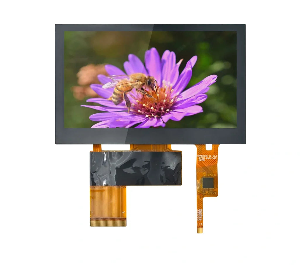
Touch screen models also need to consider the light transmittance parameter. The transmittance of optically bonded technology (about 90%) is significantly higher than that of air-gap bonding (about 80%), which directly affects the overall brightness and visual clarity of the screen.
Electrical and Interface
What kind of power supply does the display need?
The power input for a TFT module is typically a nominal value, but actual design must consider ripple and noise.
For example, for a nominal 5.0V input, the voltage should be stable within a range of ±0.25V, and power supply ripple is best kept below 50mV.
The backlight is the main source of power consumption. Driving a set of 6 LED light bars may require a current of 100mA to 1.2A, depending on the brightness and the number of LEDs.
The module typically integrates DC-DC converters and LDOs internally to provide low-voltage supplies like 1.8V and 2.5V for the LCD driver and timing controller.
Power sequencing is critical. The host controller IO voltage must be powered up before or simultaneously with the panel's analog power to avoid latch-up effects.
A typical power sequence requirement is: IO Power (VDDI) -> Analog Power (VDD) -> Positive Power Supply (AVDD) -> Negative Power Supply (VGL).
Violating this sequence may cause the display to fail to initialize or result in permanent damage.
How to choose an interface that matches the host controller?
Choosing an interface is essentially a trade-off between bandwidth, pin count, cost, and complexity.
For low-resolution screens (< 4 inches, resolution below 800x480):
-
SPI Interface: Requires only 3-4 signal lines (CS, SCLK, MOSI), clock frequency can reach 50-100MHz. But only one pixel of data can be sent per transmission, limiting the refresh rate; suitable for static UI display.
-
I²C Interface: Requires only 2 signal lines, but is slower, typically used for small OLEDs or transmitting control commands.
For medium-resolution screens (5-7 inches, 800x480 to 1024x768):
-
CPU Interface (e.g., 8080/6800 series): Uses parallel transmission, with data widths of 8 or 16 bits. Taking 16-bit 8080 parallel as an example, each clock cycle transfers 16 bits (2 bytes) of data. At a 20MHz clock, the theoretical bandwidth can reach 40MB/s. Requires a relatively high number of pins (about 20-30).
For high-resolution screens (>7 inches, 1280x800 and above) and high-speed applications:
-
RGB Interface: Directly transmits video data in RGB888 (24-bit) format to the display, synchronized with horizontal and vertical sync signals. Bandwidth calculation is: Horizontal Pixels × Vertical Pixels × Frame Rate × 24 bits. For example, 1024x768@60Hz requires about 1.13 Gbps bandwidth. Requires about 30 pins, and imposes requirements on PCB trace length matching.
-
LVDS Interface: Uses differential signals, offering strong noise immunity, suitable for longer distance transmission (e.g., from a car center console to a front display). One lane consists of 4 pairs of differential data lines and 1 pair of clock lines. The data rate per pair can reach hundreds of Mbps to several Gbps. Pin count is lower (about 10), but requires dedicated serializers and deserializers.
-
MIPI DSI Interface: The mainstream choice for mobile devices, using differential signals with low power consumption. DSI v1.2 standard single lane data rate can reach 1.5 Gbps, and multiple lanes can be bundled. 4-lane DSI total bandwidth can reach 6 Gbps, sufficient to drive 1080p@120Hz or 2K@60Hz displays. The protocol is complex, but pin count is low (clock + data requires only 3-6 pairs of differential lines).
What to note about signal integrity and routing?
PCB design for high-speed interfaces directly affects stability.
-
Impedance Matching: The impedance for MIPI and LVDS differential pairs is typically required to be controlled at 100Ω±10%. Single-ended RGB interface lines also need impedance control (e.g., 50Ω).
-
Length Matching: For the RGB interface, the length difference between data lines should be controlled within ±0.5mm. For MIPI/LVDS, the intra-pair length difference should be less than 0.1mm, and the inter-lane length difference should be less than ±2.5mm.
-
ESD Protection: ESD protection diodes near the connector are essential. Low-capacitance TVS diode arrays should be selected to ensure their junction capacitance (e.g., 0.5pF) does not excessively affect the high-speed signal edges.
Mechanical and Environmental Parameters
What parts are included in the display's physical dimensions?
Mechanical dimensions are divided into three parts:
-
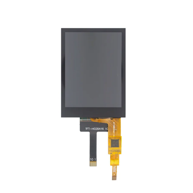
Active Area: The actual area that displays the image, e.g., 121.0mm × 36.0mm.
-
Outline Dimensions: The total space occupied, including the glass edges and driver circuit board, e.g., 126.0mm × 39.5mm × 1.8mm (L×W×H). It must be confirmed whether the thickness includes the backlight module and any additional optical films.
-
Mounting Footprint: Defines how the module is fixed. Front mounting (snapping into a panel cutout) requires confirmation of the panel cutout size (e.g., 123.0mm × 37.0mm) and the bezel's clamping width. Rear mounting (fixed by screws) requires providing the screw hole center-to-center distance, hole diameter (e.g., Φ2.2mm), and torque limit for the screws (e.g., 3~5 kgf·cm).
The position (top, bottom, left, right) and extension length (e.g., 5.0mm) of the FPC connector directly affect the internal wiring space and bending radius within the device.
ZIF (Zero Insertion Force) connectors require operational space for the flip lever, while board-to-board connectors have strict tolerance requirements for the PCB's mounting height.
How to ensure normal operation in different temperature environments?
Temperature parameters are considered at three levels:
-
Operating Temperature: The ambient temperature range within which the module can start up and operate stably. At -20°C low temperature, the viscosity of the liquid crystal material increases, response time slows down, potentially causing smearing. At +70°C high temperature, backlight brightness may decay due to reduced LED efficiency, and the driver IC may trigger internal protection due to overheating.
-
Storage Temperature: The temperature range within which the module can be safely stored in a powered-off state, typically wider than the operating temperature (e.g., -40°C to +85°C).
-
Thermal Shock Test: Evaluates the module's ability to withstand rapid temperature changes, e.g., 100 cycles between -40°C and +85°C, 30 minutes per cycle.
What does the Ingress Protection (IP) rating specifically mean?
The IP rating consists of two digits:
-
First Digit (Solid Particle Protection): IP5X indicates dust protected; it cannot completely prevent dust ingress, but the amount that enters does not interfere with normal operation. IP6X indicates complete dust tightness.
-
Second Digit (Liquid Ingress Protection): IPX4 protects against water splashing from any direction. IPX7 means it can withstand immersion in 1 meter of water for 30 minutes. Modules achieving IP65 or higher typically require full lamination using optical adhesive (OCR/OCA) and the use of sealing gaskets at the connectors.
How much vibration and shock can the module withstand?
Vibration and shock specifications simulate mechanical stress during transportation, installation, and daily use.
-
Random Vibration: A common test condition is a frequency range of 5Hz to 500Hz, acceleration of 1.5 Grms, duration of 1 hour per axis.
-
Mechanical Shock: The test condition might be a half-sine wave, peak acceleration of 50G, pulse width of 11ms, 3 shocks in each of the six directions along three axes.
How is long-term use reliability measured?
Reliability is quantified through lifespan testing:
-
Backlight Lifespan: Typically defined as the time for brightness to decay to 50% of its initial value. At room temperature and rated current, the lifespan of white LED backlights is usually 20,000 to 50,000 hours. Near the end of life, the color temperature may shift (e.g., from 6500K to 6300K).
-
High Temperature/Humidity Operating Test: Operating under power for 500 hours at 60°C temperature and 90% relative humidity. After testing, it must be confirmed that there is no corrosion, no liquid crystal contamination, and display functions are normal.
The surface hardness of the display is usually indicated by pencil hardness (e.g., 3H). Surface optical treatment (e.g., Anti-Glare AG coating) reduces specular reflectivity from about 5% to below 1%, improving visibility under strong light.
Interfaces
The TFT display interface is the pipeline for data transmission. Its selection directly determines the performance ceiling and implementation complexity of the system.
The difference in interface bandwidth can span three orders of magnitude, from about 10 Mbps for SPI to over 10 Gbps for MIPI DSI.
For example, driving an 800x480@60fps screen requires approximately 220 Mbps of bandwidth, which immediately rules out SPI and low-speed MCU interfaces.
The choice involves not only speed but also pin count (from 3-4 for SPI to 20+ for RGB), controller load, and overall BOM cost.
Parallel Interfaces
RGB Interface Drives Pixels Directly
In this mode, the host controller handles all rendering tasks. It needs to continuously generate a pixel clock signal and send 24-bit RGB data (8 bits red, 8 bits green, 8 bits blue) onto the data bus every clock cycle.
Synchronization signals control the precise timing of the image: HSYNC marks the start of a new line, VSYNC marks the start of a new frame.
Taking a 1024x768 resolution at 60Hz refresh rate as an example, the pixel clock frequency needs to reach 1024 * 768 * 60 ≈ 45MHz, and the required bandwidth is approximately 45MHz*24bit=1.08Gbps.
This real-time data stream requires the host controller to have sustained output capability. Any transmission interruption will cause display abnormalities, such as screen tearing or flickering.
The advantage is extremely low latency, suitable for dynamic content display; the disadvantage is the high performance requirement on the host controller and the large number of I/O pins required (typically over 28).
MCU Interface Relies on Local Buffer
This type of interface integrates a frame buffer and a display controller on the display module itself.
The host controller only needs to write new frame data to the display module's memory when the image updates; the local controller then autonomously handles the screen refresh.
Taking a 16-bit MCU interface as an example, each transmission contains RGB data in 565 format (5 bits red, 6 bits green, 5 bits blue).
Since the host controller resources are freed after data is written, this interface significantly reduces the performance requirement on the host.
It is suitable for static screens or applications with low update frequency, such as instrument interfaces.
However, its internal bus bandwidth limits the maximum refresh rate, and write latency may occur at high resolutions.
Electrical Characteristics and Signal Integrity
The physical layer design of parallel interfaces directly affects system stability. Taking the 3.3V LVCMOS level standard as an example, strict requirements for setup time and hold time must be considered.
For instance, the data signal must be stable for at least 3ns before the clock edge (setup time) and remain stable for at least 1ns after (hold time).
Routing rules include:
-
Data line length matching controlled within ±5mm
-
Clock signals use guard traces to reduce crosstalk
-
Termination resistor values selected based on transmission line characteristic impedance
Bandwidth Calculation in Practical Applications
Taking an 800x480 resolution @60fps display requirement as an example:
-
Total pixels: 800 * 480 = 384,000 pixels/frame
-
Pixels per second: 384,000 * 60 = 23.04 Megapixels/second
-
Considering blanking intervals, the actual pixel clock required is about 30MHz
-
With 24-bit color depth, the bandwidth requirement is 30MHz * 24bit = 720 Mbps
This calculation method determines the interface selection. When the required bandwidth exceeds 500 Mbps, an RGB interface solution is typically needed.
Power Consumption and Thermal Considerations
The capacitance per I/O pin is approximately 10pF. When switching at 3.3V and 50MHz, the dynamic power consumption of a single signal line is C*V²*f = 10pF*(3.3V)²*50MHz ≈ 5.4mW.
The total signal power consumption for a 28-bit interface can reach 150mW, not including the power dissipated by termination resistors.
Serial Interfaces
How the SPI Interface Works and Its Limits
SPI operates in a master-slave mode, with communication synchronized by a clock signal (SCLK) generated by the master controller.
Data is output via the MOSI (Master Out Slave In) line and input via the MISO (Master In Slave Out) line.
For a typical SPI TFT display, the communication is unidirectional; the master controller sequentially sends command bytes and data bytes.
SPI's bandwidth is its main limitation. The calculation formula is: Bandwidth (bps) = Clock Frequency (Hz).
However, due to protocol overhead (like command bytes, address bytes) and the display's response time, the effective bandwidth is typically only 60-70% of the theoretical value.
For example, at an 80 MHz clock frequency, the theoretical bandwidth is 80 Mbps, but the actual bandwidth available for pixel transmission might only be about 50 Mbps.
This limits its use to low-resolution screens (e.g., 320x240) with limited refresh rates.
Differential Signaling and Packet Transmission in MIPI DSI
MIPI DSI does not transmit raw pixel streams; it uses a packet-based communication protocol.
It packages pixel data, commands, and control information into standard format packets for transmission.
The physical layer uses Low-Voltage Differential Signaling. Each lane consists of a pair of differential lines (D+ and D-), offering excellent common-mode noise immunity.
DSI supports several operating modes:
-
High-Speed (HS) Mode: Used for active display refresh. The differential signal swing is about 200mV, and speeds can reach up to 2.5 Gbps per lane.
-
Low-Power (LP) Mode: Used for command transmission or static frame display. The signal swing is about 1.2V, the rate is lower, but power consumption is significantly reduced.
The total bandwidth of a four-lane DSI configuration can easily exceed 10 Gbps, sufficient to drive high-resolution, high-refresh-rate displays.
Its complexity lies in link initialization, error correction, and power state switching.
Continuous Signaling and Lane Usage in LVDS
LVDS is also a differential signaling technology, but it typically transmits data as a continuous signal stream.
It uses a process called serialization to convert parallel data (e.g., 21 or 28 bits) into a high-speed serial bitstream.
At the receiver end, a deserializer converts the data back to parallel format.
To transmit RGB data, sync signals, and clock, the LVDS interface uses multiple lanes. A typical configuration includes:
-
3 data lanes, each transmitting 7 bits of serialized data.
-
1 clock lane.
LVDS lane speeds typically range from hundreds of Mbps to several Gbps. By using multiple data lanes, the total bandwidth can meet the needs of various resolutions from 1080p to 8K.
Its stability relies on strict impedance control (typically 100 ohms differential impedance) and length matching requirements.
Signal Integrity Design Considerations
The higher the speed of the serial interface, the stricter the signal integrity requirements. Main challenges include:
-
Insertion Loss: As frequency increases, the loss from PCB substrate and connectors worsens signal attenuation. For signals exceeding 5 Gbps, higher-grade laminates (like M6 or M7) may be necessary.
-
Return Loss: Caused by impedance discontinuities, minimized by optimizing routing, using appropriate connectors, and termination matching.
-
Crosstalk: Interference occurs between high-speed differential pairs, requiring isolation by adjusting trace spacing and using ground planes.
Power Management and Efficiency
Power efficiency is a key advantage of serial interfaces. Taking MIPI DSI as an example, its power management strategies include:
-
Dynamic Clock Gating: The clock can be gated off during gaps in video stream transmission to save power.
-
Low-Power States: When the screen displays a static image, it can switch to a very low-power mode, waking up only when an update is needed.
-
Inherent Low Power of Differential Signals: Due to the small voltage swing, the dynamic power consumption during switching is relatively low.
Selection Guide
Step 1: Calculate Actual Bandwidth Requirement
Bandwidth requirement is determined by three parameters: resolution, refresh rate, and color depth. The calculation formula is: Width × Height × Refresh Rate × Bits per Pixel × Overhead Factor.
For example, for an 800×480 resolution, 60Hz refresh rate, 24-bit true color (24 bits per pixel) display requirement, considering a 20% blanking overhead, the calculation is: 800 × 480 × 60 × 24 × 1.2 ≈ 663 Mbps.
Available bandwidth ranges for different interfaces:
-
SPI Interface: Effective bandwidth typically below 80 Mbps
-
MCU Parallel Interface: Bandwidth range approx. 100-400 Mbps
-
RGB Interface: Bandwidth can reach 500 Mbps - 2 Gbps
-
MIPI DSI / LVDS: Single lane 1-2.5 Gbps, multi-lane can exceed 10 Gbps
Step 2: Evaluate Host Controller Hardware Support
Check the display subsystem chapter of the host controller datasheet. Common support scenarios include:
-
Low-cost MCU: May only support SPI or 8/16-bit MCU interface.
-
Application Processor: Typically supports RGB interface and MIPI DSI.
-
FPGA: Configurable to support various interfaces like LVDS, RGB.
If the host controller lacks native support for the required interface, consider adding a bridge chip. For example, using an RGB-to-LVDS chip adds $1.5-$3 to the BOM cost and increases PCB layout complexity.
Step 3: Analyze System Resource Constraints
-
Pin Count: SPI requires 3-4 pins, MCU interface requires 16-24 pins, RGB interface requires 28+ pins.
-
PCB Board Space: Differential interfaces (like MIPI DSI) require trace widths of 4-5 mils, single-ended interfaces require 8-10 mils.
-
Power Budget: SPI interface static power is about 10-20 mW, RGB interface at 720p resolution can consume 200-300 mW.
Step 4: Consider Environmental Adaptability Requirements
Industrial and automotive grade applications need to focus on:
-
Temperature Range: Commercial grade 0-70℃, Industrial grade -40-85℃, Automotive grade -40-105℃.
-
Noise Immunity: LVDS and MIPI DSI, using differential signals, offer better stability in noisy environments compared to single-ended interfaces.
-
Transmission Distance: For on-board transmission (<30cm), any interface can be used. For cable transmission (>30cm), LVDS is recommended.
Step 5: Evaluate Development Resources and Time
-
Driver Development Difficulty: Driver development effort for SPI and MCU interfaces is about 2-4 person-weeks; MIPI DSI may require 4-8 person-weeks.
-
Debugging Tool Requirements: MIPI DSI requires a dedicated protocol analyzer, costing $10,000-$30,000.
-
Certification Requirements: If the product needs export, MIPI DSI interface may require patent licensing fees.
Interface Selection Comparison Table
| Application Scenario | Resolution Requirement | Recommended Interface | Reasoning | Estimated BOM Cost Impact |
|---|---|---|---|---|
| Portable Medical Device | 320x240 - 480x272 | MIPI DSI | Low power, strong noise immunity | Increase $0.5-$1 |
| Industrial HMI | 800x480 - 1280x800 | RGB or LVDS | High real-time performance, good reliability | Base configuration |
| Automotive Instrument Cluster | 1920x720 and above | LVDS | Stable for long-distance transmission | Increase $2-$3 |
| Consumer-grade IoT | 240x240 and below | SPI | Cost-optimal, easy to implement | Lowest cost solution |
Implementation Checklist
-
Confirm calculated bandwidth requirement and reserve 30% margin.
-
Verify interface support capability in the host controller datasheet.
-
Evaluate PCB board space and layer count budget.
-
Confirm that thermal management measures meet power requirements.
-
Plan debugging and verification strategy.
-
Evaluate supply chain stability for mass production.
Weiterlesen
Custom TFT screens can precisely match performance requirements, such as industrial-grade wide temperature range (-30℃ to 80℃) and high brightness (1000 nits), but involve high development costs (N...
The core advantage of custom OLED lies in image quality. Its self-emitting pixels can achieve infinite contrast ratio and more vivid colors, but the cost is typically 30%-50% higher than TFT of the...
Hinterlasse einen Kommentar
Diese Website ist durch hCaptcha geschützt und es gelten die allgemeinen Geschäftsbedingungen und Datenschutzbestimmungen von hCaptcha.