


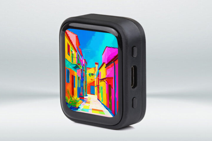
How Much Does AMOLED Module Cost
AMOLED module costs hinge on size and application—a 1-inch watch panel fetches 8, while 6.5-inch phone modules average 22. Most goes to the OLED panel (~60%), plus driver chips/touch layers; budget suppliers might drop it to 18 for entry-level phones.
Component Cost Breakdown
AMOLED module component costs split clearly: the OLED panel takes ~60%, driver ICs 15-20%, touch sensors 8-12%, with the rest going to FPC, substrates, and glue. A 6.5-inch phone module’s core parts sum to 14 before assembly.
For a 6.5-inch phone panel, the OLED layer costs 50 alone.That’s because each square inch of the organic material (small molecules or polymers) runs 1.8, and a 6.5-inch panel has ~28 square inches of active display area. Then the substrate: most phone panels use polyimide (PI) instead of glass because it’s flexible (needed for curved screens) and cheaper—PI is 15-20% less than glass, so a 6.5-inch PI substrate costs 2. Encapsulation is another 3. Oh, and size matters a lot: a 1-inch smartwatch panel’s OLED layer is only 0.2 per piece but you pay more for precision cutting (round corners aren’t easy to mass-produce), so the total panel cost for a watch is 4.
High-end phones with 120Hz refresh rates and 2K resolution need fancyICs: 2.2 per chip—they have 2 million+ transistors to handle all those pixels (vs. 500k for a 720p screen). Mid-range phones with lower specs get cheaper ICs: 1.2 each—still a big bite out of the 14 core cost for a 6.5-inch module.
Cost per square inch: 0.7—so a 6.5-inch panel adds 2.7 for touch. In-cell is an option for premium phones, but it’s harder: you stack touch electrodes right on the display, which can interfere with OLED performance if not done right.
Each FPC costs 0.5: more ports (for fast charging, multiple cameras, or speakers) mean more wires, so higher cost.
Each square meter of OCA costs 30, but if you mess up application (too much/too little glue), you get bubbles or delamination. Makers spend extra on automated glue dispensers to keep yield high.
If a panel line has 85% yield, 15 out of 100 panels are scrap. Boost that to 90%? You save 1.2 per panel.
Abudget 6.5-inch phone AMOLED module. Panel: 1.5 (15%). Touch sensor: 0.4 (4%). Substrates/glue: 13.90—close to the 14 core cost we said earlier. Add assembly (0.5), and you get a module cost of $15.90.
Panel Making Expenses
Panel making eats ~60% of AMOLED module cost: deposition tools run 10M, Class 1000 cleanrooms add 15% to overhead, and testing weeds out 10%-12% of defective panels before they hit assembly lines.
Panel making is where most of your AMOLED module’s cost comes from 60%. These things cost 10 million apiece, and a single production line might use 10-15 of them. Why so much? Because they have to evaporate organic molecules onto a polyimide substrate (standard for flexible phones) with micrometer precision—if the OLED layer is 1% too thick, pixel brightness drops by 5%, making the panel unusable. Yield here is critical: if your deposition chamber isn’t calibrated right, you lose 8%-10% of panels immediately. Boost that yield to 95%? You cut scrap costs by 0.70 per panel.
OLEDs degrade in air in hours: 5-7 stacks of aluminum oxide (Al₂O₃) and polymer films, each deposited in a separate machine. Each TFE layer costs 0.15 per square inch, so a 6.5-inch panel’s encapsulation runs 2.80. Pinholes are a silent killer—even a 1-micron hole lets oxygen seep in, wrecking the panel. Manufacturers use X-ray inspection after every layer, adding 3-$4 in deposition.
Then there’s testing, where you weed out duds before they reach your phone. First, automated optical inspection (AOI) scans panels at 100 frames per second for dead pixels or misaligned layers—costs 0.08 per panel and knocks out another 4%-5%. Together, testing removes 10%-12% of bad panels—so you don’t waste 20 assembling a broken module. Skip testing? You’ll face 15% more customer returns—costing 10x more than the $0.18 per panel testing fee.
Don’t overlook cleanroom overhead. Deposition and encapsulation need Class 1000 cleanrooms—fewer than 1000 particles >0.5 microns per cubic foot. Running one costs 30 per square foot yearly. A typical panel line uses 5,000 sq ft—adding 150k annually, or 0.20 per panel. Cut corners with a Class 10k cleanroom? Scrap rates double.
Let’s tally a 6.5-inch panel with real numbers: deposition (2.50, 32%), testing (0.18, 2%), substrate prep (7.50). At 85% yield, you scrap 15% of that cost, so goodpanel cost is 8.82. Hit 90% yield? Cost drops to 0.49 per panel. Over 1 million units, that’s $490k saved enough for 5-10 new deposition machines.

Size’s Role in Pricing
A 1-inch smartwatch panel costs 4, while 6.5-inch phone modules hit 18. Cost isn’t linear: 6.5-inch panels are ~42x larger than 1-inch, but price is just 3-4x higher because bigger sizes slash yield and complicate manufacturing.
A 1-inch smartwatch panel has ~0.87 square inches of active display area; its total cost is 4, so 4.60 per square inch. Now a 6.5-inch phone panel: 28 square inches, costing 18—0.64 per square inch. A 6.5-inch panel needs 32x more organic material than a 1-inch one, but yield drops from ~90% (small screens) to ~85% (larger ones). So for every 100 6.5-inch panels produced, 15 are scrap. That pushes the effectivecost per good square inch to 0.75, still cheaper than smartwatches but not proportional to area.
Next, yield killers. Small screens (1-2 inches) have higher yield because defects are easier to spot and discard early. A 1-inch panel line might scrap 10%. But a 6.5-inch line? Scrapping 15% hits harder because each panel costs more to make upfront. Manufacturers use laser trimming to cut off defective edges, but that adds 0.15 per panel and wastes 3%-5% of material. Skip trimming? You’ll have 5% more dead-on-arrival panels.
For a 1-inch panel, the chamber coats a small area quickly, so material waste is minimal—maybe 2%. For a 6.5-inch panel, the same chamber has to coat a much larger area evenly. If the machine isn’t calibrated perfectly, you waste 5%-7% of organic material per run. Over a year, that adds 0.30 per panel. Multiply by millions? That’s 300k wasted.
A vacuum deposition machine can process 100 1-inch panels per hour, but only 20 6.5-inch panels. So labor, energy, and machine time per 6.5-inch panel is 5x higher adding 0.70 to cost.
Material cost: 1.20, substrate 0.20, glue 1.80 / 0.9 = 0.50. Total: 3-8.00 (OLED 1.50, touch 0.70). Yield: 85%, so effective material cost: 9.41. Testing/scrap: 10.41, matching our earlier 18 range.
Makers optimize size costs by: 1) Using simpler OLED stacks for small screens (fewer layers = lower material waste), 2) Investing in AI-driven defect detection for large panels (boosts yield by 2%-3%), or 3) Limiting edge trimming for mid-size screens (saves 25-$30—because yield drops to 80%, and material waste hits 10% from larger deposition areas.
Supplier Price Variations
Supplier prices for AMOLED modules swing 15%-25% based on who makes them—Chinese vendors like BOE charge 15 for 6.5-inch phone panels, Samsung Display asks 18, and smaller regional players undercut by 10%-15% (but with 5%-8% higher scrap rates).:
Why Prices Vary: Key Factors
Samsung’s 6.5-inch lines hit ~92% yield—92 out of 100 panels ship as good. A small Chinese vendor? 85% yield. For every 100 panels:
-
Samsung wastes $0.80/panel in scrap.
-
The small guy wastes $1.50/panel.
That 7% gap slashes Samsung’s effective material cost to 9.00 upfront) vs. the small vendor’s 8.00 upfront). Higher yield lets Samsung spread fixed costs (like $5M deposition machines) over more good panels.
Next, tech tiers separate players.
-
Samsung: Offers In-cell touch (saves space) for flagships—adds 0.50/panel but justifies 18 pricing.
-
BOE: Targets mid-range with On-cell touch (cheaper, thicker) —saves 1-$2.
-
Small vendors: Skip advanced encapsulation (use thinner films) —cuts 12 panel? Expect 5% more dead screens—costing $0.60/panel in returns.
Big vendors (Samsung/LG) lock long-term deals with material suppliers (e.g., Merck for organics)—buying materials 8%-10% cheaper than small vendors. For a 6.5-inch panel, that’s 0.70 saved/panel on materials. Labor costs add to this: Chinese lines pay 7/hour vs. 20 in South Korea—saving 3/panel, letting small vendors undercut by 2.00.
|
Supplier |
Price Range |
Yield |
Tech Feature |
Scrap Rate |
Target Market |
|---|---|---|---|---|---|
|
Samsung Display |
18 |
92% |
In-cell touch |
8% |
Flagship phones |
|
BOE |
15 |
88% |
On-cell touch |
12% |
Mid-range phones |
|
Small Vendor |
13 |
85% |
Basic encapsulation |
15% |
Budget phones |
Why It Matters for Buyers
Budget phones (13): good yield (88%), decent lifespan. Flagships (17): In-cell touch, 92% yield, better brightness.
Cost Cutting Approaches
AMOLED makers slash module costs by boosting yield 5% (saves 1.20/panel), switching to inkjet printing (cuts deposition costs 30%), and ditching In-cell for On-cell touch (saves $0.40/panel). These aren’t gimmicks—they’re proven tweaks that drop costs 10%–15% without making screens look or feel “budget.”
Every 1% increase in good panels means fewer duds eating into your material budget~0.15 saved per panel. AI defect detection helps: Samsung uses computer vision to spot 1-micron pinholes in deposition layers, cutting scrap by 3% and lifting yield from 90% to 92%. For a 6.5-inch panel line cranking out 1 million units/year, that’s 300k/ year on scrapped panels.
Polymer OLEDs (used in budget screens) cost 1.50 for small-molecule OLEDs (flagships)—15% cheaper. A 6.5-inch panel saves 2 on the module. Thinner encapsulation works too: 5-layer thin-film encapsulation (TFE) instead of 7 layers cuts encapsulation cost from 1.90
720p phones need 2 OLED layers vs. 3 for 1080p—cuts deposition time by 33% and saves 0.40/panel cost of In-cell (touch embedded in the panel)—and 99% of users don’t notice the 0.3mm thicker bezel. Narrower bezels help too: reducing width from 3mm to 2.5mm cuts substrate usage by 10%—$0.30 saved/panel .”
Finally, optimize your supply chain. Long-term contracts with material suppliers like Merck lock in 8% discounts— 2.00 saved/panel (labor is 15% of module cost). And bulk purchasing with other clients slashes shipping costs by 15%—$0.10 saved/panel.
To see this in action, compare two 6.5-inch panels:
-
Flagship (Samsung): Yield 92%, In-cell touch, 3 OLED layers—cost $17.
-
Budget (BOE): Yield 88% (up from 85%), polymer OLEDs, On-cell touch, 2 OLED layers—cost $13.
BOE’s savings come from:
-
Boosting yield 3% ($0.40/panel).
-
Using polymer OLEDs ($2.00/panel).
-
Simplifying to On-cell ($0.40/panel).
-
Local assembly ($1.00/panel).
Here’s a quick recap of where the savings live:
|
Tactic |
Cost Save per Panel |
Key Detail |
|---|---|---|
|
Boost Yield 5% |
1.20 |
Fewer duds = more revenue from same material |
|
Inkjet Printing |
30% of deposition |
Cheaper than vacuum evaporation |
|
On-Cell Touch |
$0.40 |
Skips embedded touch layer |
|
Polymer OLEDs |
15% of material |
Cheaper than small-molecule OLEDs |
|
Local Substrate Sourcing |
$0.12 |
Faster lead times + lower cost |
Weiterlesen
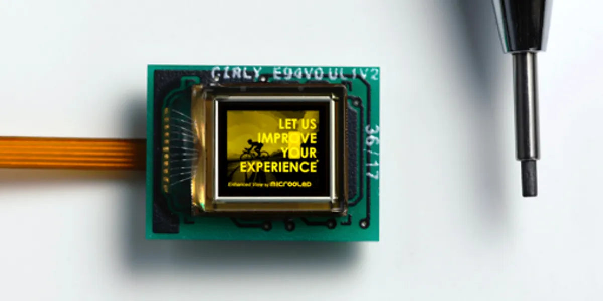
A Micro OLED display module, a compact self-emissive microdisplay, typically measures <0.5 inches diagonally with high pixel density (up to 2000 PPI), using silicon substrates for vivid, low-pow...
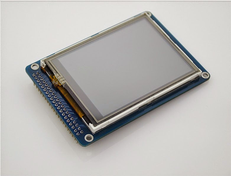
While TFT LCD serves as a basic panel tech (common in budget devices), IPS modules outperform as a premium TFT variant: they deliver a near 178-degree viewing angle (vs. TFT’s typical 140-160 degre...
Hinterlasse einen Kommentar
Diese Website ist durch hCaptcha geschützt und es gelten die allgemeinen Geschäftsbedingungen und Datenschutzbestimmungen von hCaptcha.