How to Choose OLED Display | Size, Brightness & Interface Guide
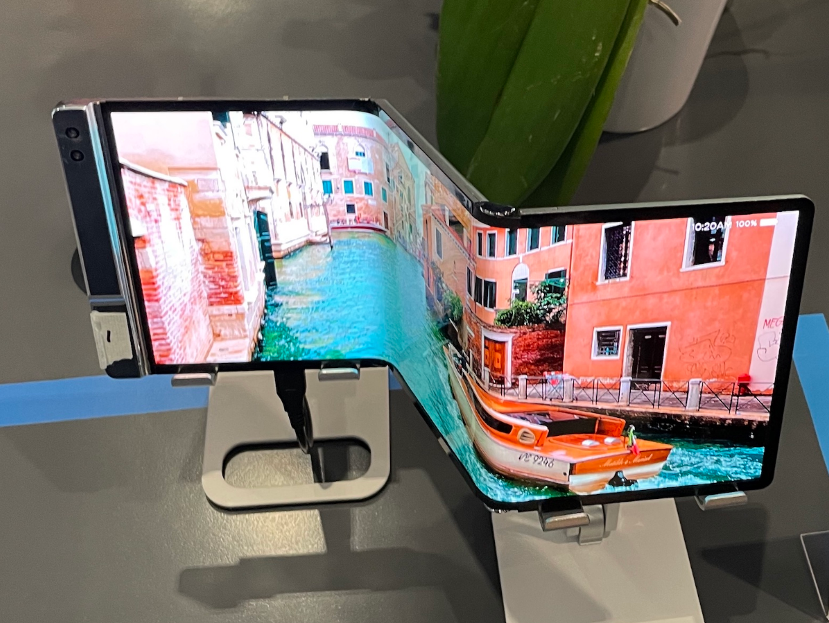
Size should be selected according to the scenario: 6.1-6.7 inches for smartphones (e.g., iPhone 15 Pro 6.1 inches, comfortable grip), 55-75 inches for TVs (65 inches for a 3-meter living room distance, formula:
Size ≈ Distance × 40), and 10-15 inches for automotive use (12.3-inch center consoles are mainstream).
For indoor use, typical 300-500 nits (iPhone 15 Pro 500 nits); outdoor requires 800 nits+ (Samsung S24 Ultra 2600 nits peak); for HDR content, choose 1000 nits+ (LG C3 TV peak 2000 nits).
Use USB-C for phones/laptops (supporting DP Alt Mode, such as Thunderbolt 4 at 40Gbps), HDMI 2.1 for TVs/game consoles (48Gbps bandwidth, 4K 120Hz), and DisplayPort 1.4 for PCs (32.4Gbps).

Size
Selecting OLED size requires benchmarking against the AA Area (Active Area) and the VA Area (Viewing Area).
Commonly used are 0.42" to 3.5" modules, with thicknesses usually between 1.2mm to 1.5mm.
When selecting a model, the aspect ratio of 1:1 or 2:1 must be calculated to adapt to the SRAM capacity of the driver IC.
For example, the AA area of a 0.96" screen is approximately 21.74 x 10.86 mm.
If the mechanical window tolerance is less than 0.2mm, it can easily cause edge pixel occlusion or light leakage.
Viewing Distance
Different Application Scenarios
Different industrial and consumer electronics scenarios have varying requirements for size and density redundancy:
| Application Category | Viewing Distance (cm) | Suggested Min Size (inch) | Resolution Requirement | Pixel Pitch (mm) |
|---|---|---|---|---|
| Smart Ring/Wearable | 15 - 20 | 0.42" | 64x32 | <0.12 |
| Handheld Analyzer | 30 - 40 | 0.96" - 1.3" | 128x64 | 0.15 - 0.20 |
| Medical Monitor | 70 - 100 | 2.4" - 3.5" | 320x240 | 0.22 - 0.30 |
| Automotive Aux Display | 60 - 80 | 1.5" - 2.0" | 128x128 | 0.18 - 0.25 |
Font Size
According to the ANSI/HFS 100-1988 standard, in a workplace environment, the minimum visual height of characters should be no less than 16 arc minutes.
- Minimum Readable Height: At a 40cm observation distance, the physical height of characters should be at least 1.86mm.
- Pixel Conversion: If a 0.96" (128x64) screen is used, its vertical pixel density is approximately 5.9 pixels per millimeter.
- Line Height Allocation: Displaying a clear English letter requires an 8x8 pixel matrix, which translates to a physical height of approximately 1.35mm. This is below the ANSI standard, so at a 40cm viewing distance, users would need to squint to read.
- Optimization Strategy: To comply with ergonomics, a 1.3" (128x64) screen should be selected. Its pixel pitch increases to 0.23mm, and the same 8x8 pixel character height will reach 1.84mm, just crossing the comfort threshold.
Brightness and Contrast
The contrast constant (>10,000:1) of OLED allows for higher perceived clarity at lower PPI compared to LCD.
- Black Level Contribution: Since OLED pixels have 0 current when turned off, the background appears perfectly black. This enhances the micro-contrast of character edges, allowing a 120 PPI OLED to visually match the physical clarity of a 150 PPI LCD.
- Irradiation Effect: Under high brightness, light-colored pixels "bleed" into surrounding dark-colored pixels. If dense text is displayed at maximum brightness (>400 nits) on a small screen (e.g., 0.42"), the physical gaps between pixels will be covered by the halo, actually causing a decrease in resolution. It is recommended to limit brightness to 60%-70% of the rated value on micro-screens with extremely high PPI to maintain text edges.
In the absence of specific UI mockups, following these empirical values can avoid most visual mismatch issues:
Handheld Mobile Devices
Prioritize 128-160 PPI.
Fixed Industrial Panels
Prioritize 0.25mm - 0.35mm pixel pitch.
Ultra-low Power Monitoring
Prioritize 0.66" - 0.91" low-resolution modules (128x32).
Power Consumption and Luminous Area
Driver IC
Regardless of the screen size, driver chips (such as SSD1306, SH1106) have inherent current overhead in an active state.
- Logic Current (Idd): Usually between 150µA to 300µA, used for processing SPI/I2C communication, SRAM addressing, and timing control.
-
Display Driving Current (Icc): This is the static consumption after the charge pump boosts low voltage (3.3V) to high voltage (7V-12V).
Even if the screen display content is minimized (e.g., displaying only one pixel), the driver IC still generates a base current occupancy of 1mA - 2mA to maintain row/column scanning timing. In miniaturized device selection, this "fixed cost" makes large-size screens exhibit extremely low efficiency ratios when displaying simple content compared to small-size screens.
OPR
- Power Differences in Inverted UI: On a 1.3" (128x64) screen, the total current for white-on-black text (approx. 10% OPR) is about 5mA. If switched to black-on-white (approx. 90% OPR), the current will instantly surge to over 30mA.
- Multiplicative Effect of Size and OPR: In large-size selections (e.g., 3.5"), even if OPR increases by only 5%, the actual absolute current increase may exceed the total power consumption of a small-size screen (0.49").
- Peak Current Management: When designing power circuits, a margin of 1.5 times the peak current at 100% OPR must be reserved to prevent system voltage drops (Brown-out) during large-area white transitions.
Brightness, Size, and Lifespan
An increase in the luminous area not only changes the current value but also changes the heat distribution.
- Thermal Density Deviation: Although a 0.42" micro-screen has low total power consumption, the heat power per unit area is higher because the light-emitting points are highly concentrated in an extremely small area. Under continuous high-brightness (>300 nits) driving, local temperature increases will lead to faster degradation of organic materials.
- Advantages of Large Size: When the same total luminous flux (lumens) is required, choosing a larger size (e.g., 2.4") and reducing the brightness per unit area provides better heat dissipation than a small-size high-brightness solution, significantly extending the half-life (LT50).
- IR Drop Loss: As size increases, the ITO (Indium Tin Oxide) traces on the glass substrate become longer, and resistance increases accordingly. For OLEDs of 3.5" and above, high current through long-distance ITO lines produces significant IR drops, and this energy is dissipated as heat, resulting in lower energy conversion efficiency for large-size screens compared to small-size modules.
Charge Pump
Most monochrome OLED modules have built-in charge pump circuits that boost the 3.3V provided by the system to the VCC (usually 9V or 12V) required for light emission.
- Efficiency Loss: The conversion efficiency of a charge pump is usually between 60% - 85%.
- Size Correlation: The larger the size, the higher the required VCC current. when the current exceeds 20mA, capacitor charging/discharging losses and internal resistance losses within the charge pump will rise significantly.
- Design Avoidance: For selections above 2.0", it is recommended to discard the built-in charge pump and use an external independent DC-DC boost circuit instead. This can improve power efficiency by 10% - 15%, offsetting some of the power consumption increase brought by large-area displays.
The impact of frame rate on power consumption varies across different sizes.
Data Load
A 2.4" 320x240 resolution screen requires processing approximately 4.6Mbits of data to refresh at 60 frames per second.
Visual Compromise
In large-size displays, low-frequency flicker is more easily perceived than on small-size screens due to larger pixels.
Therefore, large-size screens usually need to maintain a frame rate above 100Hz, which further drives up the overall system power consumption.
Meanwhile, a 0.91" screen can provide a stable visual experience at 60Hz.
Irregular Shapes and Standardization
Circular and Racetrack Shapes
- Boundary Limits of Effective Pixels: In a circular screen (e.g., a 1.28" circular screen with 240x240 resolution), edge pixels are restricted by the circular frame, so UI design must avoid the four corners. It is calculated that the actual usable pixel area of a circular screen is about 21.5% less than a square screen of the same resolution.
- Specificity of Driver Mapping: Although the physical shape is circular, the internal graphics memory (GRAM) of the driver chip (e.g., GC9A01 or similar) is still arranged in a rectangular array. The controller still sends 240x240 data, but pixels outside the circumference are physically masked at the hardware level, leading to about 20% bandwidth waste in data transmission.
- Installation Positioning and Center Deviation: Circular screens have extremely high requirements for installation precision. In structural design, the coaxiality between the glass center and the housing ring center must be considered. Usually, the center offset tolerance for standardized circular modules is ±0.15mm. If the housing opening is too tight, the visual eccentricity will be very obvious.
Bar Type
- Extreme Aspect Ratio: Common 0.91" screens have a 4:1 (128x32) aspect ratio. This specification performs excellently in environments where vertical space is extremely compressed, with glass widths usually only 10mm - 12mm.
- FPC Exit Direction: The FPC of a bar-shaped screen usually exits from the long side (Bottom Side). When selecting, attention must be paid to the FPC width. The FPC width of some 0.91" specs is almost equal to the total glass width, leaving very little space for component avoidance on the PCB.
- Driver Scan Frequency: Due to the small number of rows (only 32 rows), the duty cycle of such screens is 1/32. Compared to the 1/64 duty cycle of 128x64, bar screens can achieve higher peak brightness under the same driving voltage, usually stable at 150-200 nits.
Irregular Cutting
- Laser Cutting Edge Stress: In irregular OLEDs, micro-cracks generated at the edges during laser cutting are a cause of oxygen leakage and black spots. The sealing width for irregular specs usually needs to increase from the standard 0.5mm for rectangles to 0.8mm-1.0mm to ensure the sealing of organic materials.
- R-angle and Chamfer Requirements: If the device housing has large rounded corners, the R-angle radius of the OLED substrate must be confirmed during selection. Common standard screen R-angles are usually less than 0.5mm, while some irregular selections can achieve R=2.0mm or more, enabling a true "full-screen" visual effect.
- Cover Glass Integration: Many irregular screens come factory-pre-bonded with 2.5D or 3D cover glass. In this case, the physical size of the screen must increase by the cover glass overhang (usually 1.5mm - 3.0mm per side), which changes the product stack-up height.
Customized Sizes
When standardized sizes (e.g., 1.3" or 2.4") cannot meet specific industrial housings, developers consider custom specs.
- Glass Substrate Utilization: OLED production is carried out on large Mother Glass. If a custom size causes the mother glass cutting yield to drop from 90% to 70%, the unit cost will increase significantly. For example, slightly enlarging a size from 1.3" to 1.4" might reduce the output per mother glass by an order of magnitude.
- Fine Metal Mask (FMM) Costs: Custom irregular resolutions require re-manufacturing a Fine Metal Mask. This is a significant expense, and the cost after amortization is usually competitive only when single purchase volumes reach 50K - 100K pieces or more.
- Supply Chain Risk: Irregular screens are often from a Single Source. Over a long supply cycle, if the supplier stops production or upgrades the line, the difficulty of finding a replacement and the cost of redesign will far exceed standardized specs.
Standard OLED specs cover regular ratios like 1:1, 4:3, 16:9, with common diagonals at 0.91", 0.96", 1.3";
their supply chains are mature and feature Pin-to-Pin compatibility.
Irregular screens such as circular (diameter 0.5" - 1.5") or cut-corner screens usually have an effective area utilization of only 70% - 85% of the rectangular substrate.
Selecting irregular specs requires bearing more than 20% in Non-Recurring Engineering (NRE) fees and longer material Lead Times (L/T), but provides high-integration visual solutions exceeding 300 PPI.
Brightness
OLED brightness is limited by APL (Average Picture Level).
At full-screen white (100% APL), protected by the drive current, brightness is usually only 200-400 nits;
While at 1% APL, peak brightness can exceed 2000 nits.
Selection should focus on ACR (Ambient Contrast Ratio), reducing reflectivity to below 4% via a λ/4 circular polarizer to ensure text readability under 50,000 lux direct sunlight.
Definitions
Full-Screen Sustained Brightness
Full-screen sustained brightness refers to the highest brightness the screen can maintain stably for a long time at 100% APL (Average Picture Level, i.e., all pixels displayed in pure white).
- Technical Benchmarking: Most commercial-grade OLEDs have nominal full-screen brightness values at 100% APL ranging from 250 nits to 450 nits. Exceeding 600 nits full-screen brightness causes panel power consumption to surge above 5W-10W, triggering serious localized heating.
- IR Drop Impact: Due to resistance in the transparent conductive layer (ITO), when full-screen pixels are turned on, high current through the traces causes a voltage drop, leading to uneven brightness between the center and edges of the screen. High-end panels use Auxiliary Electrodes to reduce resistance, keeping full-screen brightness deviation within 5%.
- Application Differences: When designing a text editor or a white-background webpage, what the user perceives is this brightness. If the device is to be used in a bright indoor office, full-screen brightness must not be lower than 350 nits.
Local Peak Brightness
Local peak brightness usually refers to the highest instantaneous brightness displayed in an extremely small area (e.g., 1% or 5% APL).
- Data Performance: In HDR content playback, reflections of the sun or lights require extremely high instantaneous brightness. Peak brightness of top-tier flexible OLED modules has evolved from 1200 nits three years ago to 2500-3000 nits currently.
- Driving Logic: This high brightness is limited by the driver IC's OVP (Over Voltage Protection). If high-brightness display lasts more than a few seconds, the system will use algorithms to downregulate the current to protect the organic light-emitting materials.
- Contrast Quantization: High peak brightness combined with OLED black levels near 0.0005 nits allows for dynamic contrast ratios exceeding 1,000,000:1. When selecting, the peak brightness Window Size should be confirmed; 1000 nits in a 10% window has stronger circuit robustness than 1000 nits in a 1% window.
High Brightness Mode (HBM)
HBM is an emergency boost mode specifically designed for strong outdoor light environments.
It uses feedback from an Ambient Light Sensor (ALS) to forcibly raise the drive voltage when ambient illumination exceeds 20,000 lux (overcast outdoors) or 100,000 lux (direct sunlight).
- Trigger Mechanism: HBM usually does not provide manual adjustment options and only automatically turns on when the sensor detects strong light. This is to prevent users from accidentally draining the battery quickly or burning out the panel.
- Performance Range: HBM typical values for outdoor handheld devices should be between 800 nits and 1200 nits. If the HBM value is below 700 nits, screen content will become blurred under direct summer sunlight due to low contrast.
- Thermal Management Constraints: After turning on HBM, the panel temperature rise is usually 2°C-5°C per minute. Once the junction temperature reaches a threshold (usually 45°C), the firmware will force an exit from HBM to prevent permanent degradation of the organic materials.
100% APL full-screen sustained brightness (usually 200-500 nits) determines basic office visual perception;
1% APL peak brightness (up to 2000+ nits) determines HDR dynamic range;
HBM excitation brightness (commonly set at 800-1200 nits) determines readability in 50,000 lux environments under strong light.
APL
ABL
ABL is hard logic embedded in the Display Driver IC (DDIC).
It dynamically adjusts output voltage by monitoring pixel values in the Frame Buffer in real-time.
- Power Budget: Manufacturers usually set a maximum power limit for the module (e.g., 4.5W). When image content exceeds a certain APL threshold (usually 15% to 25%), the system begins to downregulate the driving current proportionally.
- Brightness Drop Curve: At 5% APL, the screen might maintain 1200 nits; once APL reaches 50%, brightness may decrease linearly to 600 nits; at 100% APL, brightness is often locked between 200-300 nits.
- Transient Response Time: The delay for high-performance drivers to handle ABL is usually less than 16.7ms (one 60Hz frame period), ensuring users don't perceive sharp brightness flickering when switching between light and dark scenes. However, subtle floating of background brightness can still be observed when scrolling through large-area white webpages.
Power Distribution
- Sub-pixel Energy Efficiency Gap: The luminous efficiency of blue organic phosphorescent materials is usually much lower than red and green. To synthesize pure white, blue sub-pixels need higher current densities. At 100% APL white, about 40%-50% of the energy is consumed by the blue sub-pixels.
- IR Drop: In a high APL state, current flows from the screen edge traces to the center. Due to trace resistance, center pixels receive lower voltage than edge pixels. This Vdd drop increases full-screen white brightness non-uniformity by 10%-15%.
- Leakage Current: At low APL (e.g., 1%), to maintain contrast, closed pixels must completely cut off current. Leakage current for high-spec panels must be controlled at the pA (picoampere) level to ensure power consumption in black areas is near zero.
Lifespan Impact
APL not only limits current brightness performance but also determines panel lifespan through heat accumulation.
| Content Type | Average APL Value | Power Coefficient (Nominal) | Recommended Max Brightness |
|---|---|---|---|
| Video (Standard Movie) | 15% - 25% | 1.0x | 800 nits |
| Social Media (Text/Image mix) | 40% - 60% | 2.5x | 500 nits |
| Spreadsheets/Office Docs | 80% - 95% | 4.0x | 300 nits |
| Dark Mode | 2% - 8% | 0.2x | 1200 nits |
- Hotspots Risk: When the screen runs at high APL for a long time, heat is mainly concentrated on the TFT backplane. If the thermal design (e.g., graphene sheets or aluminum alloy mid-frame) has a thermal conductivity lower than 1500 W/m·K, local temperature rises may exceed 50°C, accelerating the oxidative degradation of organic materials and causing Burn-in to appear early.
- External Compensation: Modern driver ICs record the cumulative light emission of every pixel based on APL. When APL remains high for long periods, the system fine-tunes the drive voltage via algorithms to compensate for attenuation, which further drives up power consumption.
Driver Architecture
LTPS (Low-Temperature Polycrystalline Silicon)
Has extremely high electron mobility (>100 cm²/V·s), supporting high current output at high APL, but leakage current is high under static images.
LTPO (Low-Temperature Polycrystalline Oxide)
Combines the low-leakage characteristics of oxide TFTs, supporting 1Hz - 120Hz dynamic refresh rates.
Under low-APL static images, LTPO can reduce power consumption by 15%-20%, leaving more power headroom for high-brightness ABL.
Outdoor Readability
ACR
Outdoors, the basis for the human eye to judge the clarity of screen content is the Ambient Contrast Ratio (ACR).
The calculation formula is as follows:
ACR = (L_on + L_refl) / (L_off + L_refl)
- L_on: Brightness emitted by the display (e.g., 1000 nits).
- L_off: Brightness when the screen is off (for OLED, usually considered 0 nits).
- L_refl: Brightness reflected back from the screen surface by ambient light.
The calculation of L_refl depends on ambient illumination (Lux) and reflectance.
For example, in typical 50,000 lux sunlight, if the screen reflectance is 10%, L_refl is 1592 nits.
In this case, even if screen brightness reaches 1000 nits, the ACR is only 1.62:1, making text basically unreadable.
If reflectance is reduced to 2%, L_refl drops to 318 nits, and ACR improves to 4.14:1, reaching the readability threshold.
Reflectance Control
OLED panels contain many metal electrodes (such as aluminum or silver cathodes), which have extremely high specular reflectivity.
For outdoor use, optical filtering mechanisms must be added outside the encapsulation layer.
- Circular Polarizer Structure: This is a sandwich consisting of a linear polarizer and a 1/4 wave plate (QWP). External natural light becomes linearly polarized after entering, then circular polarized after passing through the QWP. After reflecting off the metal electrode, its handedness reverses, and it becomes linearly polarized again after passing through the QWP, but its polarization direction is 90 degrees offset from the outer polarizer, causing it to be absorbed. This structure can eliminate over 95% of internal reflections.
- Anti-Reflection (AR) and Anti-Glare (AG) Coatings: AR coatings use destructive interference principles to further reduce the reflectance of the cover glass surface. High-performance AR films can further reduce reflectance from 4% to 0.5% - 1%.
- Optical Bonding: By using index-matched OCA/OCR adhesive to fill the air layer between the glass and the OLED panel, additional 4.5% interface reflections caused by sudden changes in refractive index are eliminated.
Strong Light
In high-brightness outdoor environments, ambient light not only dilutes brightness but also significantly reduces color saturation through the wash-out effect.
- Color Volume Loss: In 30,000 lux environments, due to reflected light mixing, the originally 100% DCI-P3 gamut perception of an OLED may shrink to 30%.
- Color Enhancement Algorithms: The driver IC will automatically raise the middle of the Gamma curve (Mid-tones) and over-saturate red and green when high ambient light is detected, compensating for color purity neutralized by ambient light.
- White Balance Drift: The color temperature of sunlight is approximately 5500K - 6500K, while many OLEDs have a default white point at 7500K. To maintain outdoor visual consistency, the system needs to adjust RGB gain in real-time.
In 107,600 lux (direct clear sky) environments, the screen needs to maintain an ACR of over 5:1.
OLED, through integrated λ/4 circular polarizers, suppresses surface reflectance from a native 15% to below 4%.
Combined with 1200 nits brightness generated in HBM mode, it can achieve a contrast ratio of about 8:1.
Interface Guide
Interface selection depends on bandwidth calculation ($Resolution \times Color Depth \times Frame Rate$) and the number of available GPIOs.
For simple character displays with data rates below 10fps, I2C requires only 2 pins but is limited by the 400kHz standard rate;
SPI frequency can reach over 50MHz, supporting smooth refresh at 320x240 resolution;
Specs above HVGA (320x480) usually require MIPI DSI (1Gbps+ differential signal) or Parallel RGB (16-24 pins) to prevent screen tearing.
Serial Interfaces
I2C Bus
Although the I2C standard defines 100kHz (Standard), 400kHz (Fast), 1MHz (Fast+), and even 3.4MHz (High Speed) rates, most mainstream OLED driver ICs (e.g., SSD1306, SH1106) only stably support up to 400kHz.
- Start and Stop Bits: Every transmission requires Start and Stop signals, consuming bus time.
- ACK/NACK: After every 8-bit data sent, the slave must provide a 1-bit acknowledgement signal. Transmitting 1 byte actually takes 9 clock cycles.
- Address Frame: Before writing to the graphics memory (GDDRAM), a 7-bit device address (usually $0x3C$ or $0x3D$) plus a 1-bit read/write bit must be sent.
Calculation Example:
Refreshing a 128x64 monochrome screen (1 bit/pixel) requires $128 \times 64 / 8 = 1024$ bytes.
At a 400kHz clock, the theoretical transmission time is:
$$Time_{frame} = \frac{1024 \times 9}{400,000} \approx 23.04 ms$$
The theoretical maximum frame rate is only $\approx 43 FPS$. If control command overhead is added, the actual frame rate is usually below 35 FPS.
Pull-up Resistors and Bus Capacitance
I2C is an open-drain structure and cannot output high levels; it must rely on external pull-up resistors ($R_p$).
- Capacitance Limit: I2C specifications require bus load capacitance $C_b$ not to exceed 400pF. Long ribbon cables and FPC connectors of OLED modules will significantly increase parasitic capacitance.
-
Resistor Selection: The value of $R_p$ determines the signal rise time ($t_r$). The formula is:
$$t_r \approx 0.8473 \times R_p \times C_b$$
If $C_b$ is high and $R_p$ is too large (e.g., 10kΩ), the signal rising edge will slow down, leading to timing violations, manifested as screen garbling or initialization failure. For 400kHz applications, $R_p$ between $2.2k\Omega$ and $4.7k\Omega$ is recommended.
SPI Interface Variants
4-Wire SPI (8-bit Mode)
This is the most common configuration, consisting of SCLK, MOSI, CS (Chip Select), and D/C (Data/Command) signals.
- Mechanism: The level status (high/low) of the D/C pin tells the OLED controller whether the current byte on the bus is pixel data or a configuration command.
- DMA Advantage: Pixel data is usually a continuous large block of memory. In 4-Wire mode, D/C can be pulled high, then DMA can be started to push the entire frame buffer to the SPI bus without CPU intervention.
- Clock Polarity: Most OLED driver ICs (e.g., SSD1351, ST7735) support SPI Mode 0 ($CPOL=0, CPHA=0$) or Mode 3 ($CPOL=1, CPHA=1$).
3-Wire SPI (9-bit Mode)
This mode eliminates the D/C pin, keeping only SCLK, MOSI, and CS.
- Mechanism: Every clock cycle transmits 9 bits of data. The 1st bit is the D/C flag, and the following 8 bits are the actual data.
- Software Disadvantage: Standard MCU SPI hardware peripherals usually transmit in units of 8-bit or 16-bit. Implementing 9-bit transmission usually requires software simulation (Bit-banging) or piecing together data via complex bit-shifts, causing CPU usage to skyrocket and making it difficult to utilize DMA.
- Application Scenario: Limited to micro-devices with extremely restricted pins and very low refresh rate requirements.
PCB Layout
When SPI clock frequencies rise above 40MHz, signal traces possess RF characteristics, and PCB routing must follow high-speed signal design principles.
Impedance Matching and Reflection
OLED modules are usually connected via FPC, where characteristic impedance is often not strictly controlled.
- Source Series Resistor: It is recommended to connect a $22\Omega$ to $47\Omega$ resistor in series at the MCU's SCLK and MOSI output pins. This resistor should be placed close to the MCU to slow down signal edges, absorb reflected waves, and prevent overshoot from locking up the OLED driver chip.
Crosstalk Suppression
- Ground Shielding: SCLK is the primary source of interference. In FPC pinout definitions or PCB routing, GND signals should be placed on both sides of SCLK as much as possible to form a "ground wrap" structure.
- Trace Length Limit: For single-ended SPI signals, trace lengths should not exceed 10cm. If long-distance transmission is necessary, buffers should be added or a differential signal solution should be used.
The serial interface I2C uses an open-drain architecture, requiring only SDA and SCL lines to mount multiple devices, providing an effective throughput of about 300kbps in 400kHz fast mode, suitable only for monochrome refresh below 128x64 resolution;
SPI utilizes push-pull output logic, achieving high-speed transmission of 50MHz+ via dedicated clock and data lines (3-wire or 4-wire configuration), reducing MCU load to below 5% with DMA controllers, making it the engineering first choice for driving 16-bit RGB565 color OLEDs.
Parallel Interfaces
Protocol Architecture
Intel 8080 System (System 80)
This is currently the most common parallel mode in OLED controllers.
Its control logic relies on independent "Read" and "Write" signal lines.
- Control Signals: CS (Chip Select), D/C (Data/Command), RD (Read Enable), WR (Write Enable).
- Trigger Mechanism: Data is latched by the OLED controller on the Rising Edge of the WR signal. The MCU must prepare the data bus level (Setup Time) before WR is pulled low and maintain it for a period (Hold Time) after WR is pulled high.
- Timing Parameters: Typical OLED driver ICs (e.g., ILI9341 or RM68120) require a minimum write cycle $t_{WC}$ of about 66ns, corresponding to approximately 15MHz operation frequency.
Motorola 6800 System (System 68)
- Control Signals: CS, D/C, E (Enable Signal), R/W (Read/Write Select).
- Trigger Mechanism: Read/write direction is determined by the R/W pin level; actual data transmission occurs during the high-level pulse width of the E signal.
- Engineering Status: Native support for 8080 timing in modern MCUs (such as STM32's FSMC module) is more common, leading to 6800 mode being used less in new projects.
Bandwidth Throughput
8-bit Parallel
- Transmission Logic: A 16-bit pixel (RGB565) needs to be transmitted in two parts: high 8 bits first, then low 8 bits.
- Efficiency Loss: Compared to 16-bit parallel, its theoretical bandwidth is halved.
- Suitability: Suitable for scenarios where the number of GPIOs is limited (e.g., less than 20) but SPI's low speed is unacceptable.
16-bit Parallel
- Transmission Logic: A single Write Cycle can transmit a complete RGB565 pixel.
-
Bandwidth Calculation: If $t_{WC} = 50ns$ (20MHz):
$$Throughput = 20 \text{ MHz} \times 16 \text{ bit} = 320 \text{ Mbps}$$ -
Frame Rate Evaluation: Driving a 320x480 screen (data volume approx. 300KB/frame):
$$FPS_{max} \approx \frac{20,000,000}{320 \times 480} \approx 130 \text{ FPS}$$
This leaves plenty of idle time for the MCU to perform logic operations, making it the standard configuration for 3.5-inch to 5-inch displays.
18-bit / 24-bit Parallel
- RGB666 (18-bit): Capable of showing 262K colors with smoother transitions, but requires 18 data lines. Since most MCUs have 16-bit architectures, processing 18-bit data usually requires complex bit-shifts, causing software overhead to surge, thus it's less popular than 16-bit in the embedded field.
Driver Implementation
In practice, parallel ports are rarely driven by software simulation (bit-banging) of GPIOs, as this exhausts CPU resources.
Modern high-performance MCUs utilize External Memory Controllers (FSMC/EXMC) to drive OLEDs.
-
Memory Mapped I/O: The MCU maps the OLED graphics memory (GRAM) to a section of external memory address (e.g., $0x60000000$).
- Command Address: Mapped to an address where the $A_{n}$ line is low.
- Data Address: Mapped to an address where the $A_{n}$ line is high (corresponding to the D/C pin).
-
Operation: Engineers only need to assign values to specific memory addresses (e.g.,
*(__IO uint16_t *) (0x60000000) = 0xFFFF;), and the hardware controller automatically generates the corresponding CS, WR, and RD timing. - DMA Involvement: Combined with DMA, the MCU can "move" image frame buffers from internal SRAM to the mapped external address. The entire process consumes near 0% CPU, forming the basis for high-frame-rate UI animations.
Signal Integrity
Simultaneous Switching Noise (SSN / Ground Bounce)
When 16 data lines flip from 0 to 1 simultaneously, the instantaneous current ($di/dt$) is huge.
Due to parasitic inductance in the ground loop, this causes the internal ground level of the chip to rise momentarily, leading to logic misjudgments.
- Countermeasure: Data lines should have $33\Omega \sim 47\Omega$ resistor networks in series.
- Resistors should be placed close to the MCU output to reduce signal Slew Rate, minimizing overshoot and ringing.
Length Matching
Although parallel port rates (~20MHz) are much lower than DDR memory, signal Skew still needs attention during long-distance transmission (>15cm) or when using FPC ribbon cables.
- Phenomenon: If the WR signal arrives before the data signal at the OLED, wrong data bits may be latched.
- Specification: Ensure the length difference between the WR control line and the Data bus is controlled within 500mil.
RGB Interface
When discussing parallel ports, MCU Interfaces (8080/6800) are often confused with RGB Interfaces (DPI - Display Pixel Interface).
| Feature | MCU Interface (8080/6800) | RGB Interface (TTL/DPI) |
|---|---|---|
| GRAM Location | Integrated inside panel | No internal GRAM, relies on MCU memory |
| Refresh Mechanism | MCU sends write command; screen is static | MCU must continuously send pixel stream |
| Signal Lines | WR, RD, CS, D0-D15 | VSYNC, HSYNC, DOTCLK, DE, D0-D23 |
| Scenarios | Smartwatches, instruments (static UI) | Tablets, automotive screens (video/dynamic) |
| Resolution Cap | Usually < 800x480 | Up to 1024x600 or higher |
Selection Criteria
If the host MCU memory (SRAM) is small (e.g., less than 500KB), an MCU interface screen with GRAM must be selected.
If using a high-performance SoC running Linux with MB-level memory, the RGB interface is more cost-effective (screen modules are cheaper without GRAM).
High-Speed Differential Interfaces
MIPI DSI D-PHY
MIPI DSI (Display Serial Interface) standard interface consists of 1 pair of differential clock lines and 1 to 4 pairs of differential data lines (Lanes).
Dual Mode Operation
D-PHY is unique because it mixes two distinct electrical standards:
-
Low Power Mode (LP Mode):
- Level: 0V to 1.2V single-ended signal.
- Rate: < 10 Mbps.
- Purpose: Transmitting initialization commands, putting OLED in/out of sleep, reading register states. At this time, differential pairs separate and function as two independent GPIOs.
-
High Speed Mode (HS Mode):
- Level: 200mV differential signal, common-mode voltage approx. 200mV.
- Rate: 80 Mbps to 2.5 Gbps (D-PHY v1.2) / 4.5 Gbps (D-PHY v2.0) per lane.
- Purpose: Transmitting pixel-stream video data.
Mode Switching Timing (SoT/EoT)
Switching from LP to HS is not instantaneous; it requires strict timing handshakes:
- LP-11 (Stop State) $\rightarrow$ LP-01 $\rightarrow$ LP-00 $\rightarrow$ HS-0 (Sync).
- If P/N line lengths don't match in PCB layout, the LP-00 state duration will be abnormal, causing the DSI controller to fail in locking the Sync Word, resulting in a black screen.
Video Mode vs. Command Mode
Video Mode
- Working Principle: The host (AP/SoC) must continuously send pixel data streams over the DSI bus, including H-Sync, V-Sync, and V-Active signals.
- OLED Side: No full-frame graphics memory (GRAM) on the screen module.
- Pros/Cons: Lower module cost (smaller driver IC area), but higher system power consumption because the SoC and DSI link cannot sleep even when displaying static images.
- Applications: Smartphones, tablets, video players.
Command Mode
- Working Principle: Data is sent only when the screen updates. After the host writes one frame of data to the OLED module's GRAM, transmission can stop, and the DSI link enters a low-power state.
- OLED Side: Integrated full GRAM.
- Features: Supports Panel Self Refresh (PSR). The OLED driver IC automatically reads data from the local GRAM to refresh the screen.
- TE Sync: To prevent tearing, the OLED sends sync signals to the host via a dedicated TE pin or DSI BTA (Bus Turn Around) mechanism.
- Applications: Smartwatches (Always-On Display), low-power instruments.
eDP
When screen size exceeds 10 inches (e.g., laptop OLED panels), MIPI DSI's transmission distance limit (usually < 15cm) becomes a shortcoming.
eDP is based on the DisplayPort protocol and optimized for embedded connections.
- AC Coupling: 100nF capacitors are connected in series on eDP differential lines, isolating DC bias between the transmitter and receiver. This allows the SoC and OLED panel to use different voltage references and allows for longer cable transmission (up to 30-50cm).
- Link Training: During power-on initialization, the host sends specific patterns, the receiver provides feedback on signal quality, and both parties negotiate the best Pre-emphasis and voltage swing levels to adapt to different FPC qualities and lengths.
- AUX Channel: Unlike MIPI DSI, which mixes instructions on data lines, eDP has an independent pair of low-speed bidirectional AUX channels for reading EDID, controlling backlight/OLED brightness, and touch feedback.
- PSR (Panel Self Refresh): eDP v1.3+ standards introduced PSR functionality similar to MIPI Command Mode, allowing the SoC's GPU to completely power down during static screens, relying solely on panel T-CON refresh, significantly extending laptop battery life.
Channel Planning
When choosing MIPI/eDP interface configurations, the Total Bandwidth required must be calculated.
Formula:
$$DataRate = (Width + H_{blank}) \times (Height + V_{blank}) \times FPS \times ColorDepth$$
Note:
Blanking overhead must be included, usually about 10%-15% of the effective resolution.
Example: Driving a 1080p (1920x1080) @ 60Hz, 24-bit OLED.
- Effective pixel clock $\approx 1920 \times 1080 \times 60 \approx 124 \text{ M pixels/s}$
- With Blanking (1.15x) $\approx 142 \text{ M pixels/s}$
- Total bit rate $\approx 142 \text{ M} \times 24 \text{ bit} \approx 3.4 \text{ Gbps}$
Lane Allocation:
- If D-PHY supports 1.0 Gbps per lane: 4 Lanes are needed.
- If D-PHY supports 1.5 Gbps per lane: 3 Lanes are needed (4 Lanes are often used for redundancy).
- If 2 Lanes are used, each lane must run at over 1.7 Gbps, requiring extremely high PCB routing standards.
PCB Layout
- Differential Impedance: Must be strictly controlled at $100\Omega \pm 10%$. This requires calculating line width and gap based on the PCB Stack-up. Usually, on FR4, surface microstrip width is about 4-6 mil with 4-6 mil spacing.
-
Skew Control:
- Intra-pair Skew: The length difference between P and N lines should be less than 5 mil (0.127mm). Phase mismatch turns differential signals into common-mode noise, destroying signal integrity.
- Inter-pair Skew: The length difference between clock and data channels is more lenient, usually kept within 50 mil (1.27mm). The D-PHY protocol allows data to have a certain offset relative to the clock.
- Reference Plane: There must be a complete, continuous GND Plane underneath differential lines. Do not cross split planes, as broken return paths generate severe EMI and signal distortion.
- Via: Avoid changing layers as much as possible. If necessary, place GND vias next to signal vias to provide a continuous return path. Each via produces about 1-3dB of signal loss and impedance discontinuity.
When OLED resolutions exceed WVGA (800x480) and refresh rates reach 90Hz, single-ended signals (TTL) are no longer suitable due to EMI and clock skew issues.
MIPI DSI uses low-voltage differential signals (200mV swing) and has become the preferred choice for mobile devices, providing aggregate bandwidth of 1.5 Gbps to 6.0 Gbps through 1-4 data lanes, enough to support 4K video streams.
For panels over 11 inches, eDP has replaced LVDS with micro-packet transmission and bidirectional auxiliary channels (AUX).
Weiterlesen
OLED achieves infinite contrast (>100,000:1) and refresh rates exceeding 120Hz thanks to its self-emissive characteristics, making it suitable for dynamic video; Electronic paper (ePaper) relies...
The cost of OLED modules increases non-linearly with size; 65-inch large screens have a unit price far higher than mobile phone screens due to significant cutting losses. High resolution (>400 P...
Hinterlasse einen Kommentar
Diese Website ist durch hCaptcha geschützt und es gelten die allgemeinen Geschäftsbedingungen und Datenschutzbestimmungen von hCaptcha.