


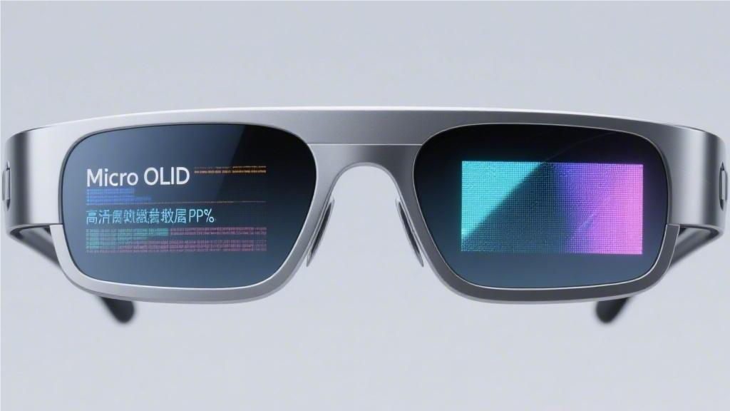
Micro OLED for Smart Glasses | Pixel Density (PPI), Weight & Power Efficiency
Micro OLED panels are the ideal choice for smart glasses.
Their pixel density reaches 3000 to 4000 PPI, presenting high-definition vision without the screen door effect;
The weight of a single screen is typically less than 3 grams, ensuring extreme lightweighting of the device;
In practical operation, combined with dynamic brightness and refresh rate adjustments, its self-illuminating power consumption can be controlled at around 200 milliwatts, thereby significantly improving battery life.
Pixel Density (PPI)
Smart glasses screens are only 2 to 3 centimeters away from the human eye.
When traditional smartphone screens (around 400 PPI) are magnified by lenses, a rough pixel grid appears.
Micro OLED uses a monocrystalline silicon wafer as the substrate, shrinking the pixel size to 4 to 10 microns, achieving a PPI of over 3000 to 4000.
For users, when wearing smart glasses to read 8-point small text or watch 4K videos, the edges of text and images are smooth, the naked eye cannot perceive pixel gaps, and the picture presents retina-level clarity.
Eliminating the Grid Sensation
The lens system of smart glasses magnifies the 0.5 to 0.7-inch micro-screen into an equivalent virtual image of over 100 inches at a distance of 3 meters. This physical magnification of about 20 times will synchronously magnify the pixels on the display module and the black gaps between pixels. On a traditional 500 PPI screen, these black gaps appear to the human eye as a dense grid, causing obvious visual interference.
The physical grid sensation originates from the "non-illuminating areas" between pixels. The driving circuits of traditional LCD or glass-based OLED occupy a large amount of space, causing the pixel fill factor to usually be below 60%. When light enters the pupil through Pancake (folded optical path) lenses, the human eye can perceive black lines with a width of about 10 to 15 microns.
Micro OLED abandons the traditional glass substrate and switches to a 28nm or 65nm semiconductor CMOS process. This processing precision allows the driving circuit to be buried directly below the pixels, rather than placed side-by-side. Through this stacked structure, the physical gap between pixels is compressed to less than 1 micron.
- Pixel Pitch: The pixel pitch of Micro OLED is reduced to 4 to 8 microns, whereas traditional smartphone screens are typically 40 to 60 microns.
- Fill Factor: The silicon-based process increases the effective light-emitting area to over 90%, greatly reducing the non-illuminating "black zones."
- Physical Density: Over 12 million light-emitting diodes are integrated per square inch, ensuring the continuity of the picture after magnification.
The metric used to evaluate the disappearance of the grid sensation is PPD (Pixels Per Degree). For adults with 20/20 vision, the resolution limit is approximately 60 PPD. If the PPD is below 20, the image looks like viewing the world through a screen door. A traditional headset using 1080P resolution has a PPD of only about 21 at a 90-degree Field of View (FOV).
Devices equipped with Sony's silicon-based Micro OLED push the PPD to between 35 and 45 at the same FOV through an ultra-high density of 3400+ PPI. Although it does not fully reach the 60 PPD limit, within the 20mm Eye Box, the naked eye can no longer capture the edges of individual pixels.
When viewing black text on a white background (such as PDF documents), the text edges on traditional screens will show obvious staircase artifacts due to the large pixels. Relying on its micron-level pixel arrangement, Micro OLED keeps text lines smooth and fluent even after optical magnification.
Image continuity plays an important role in reducing visual fatigue. When the brain cannot perceive discrete pixels, the visual center no longer needs extra filtering processing to synthesize the image. This physical-level smoothness reduces the cognitive pressure caused by prolonged use of AR devices.
In terms of sub-pixel arrangement, Micro OLED typically adopts an RGB stripe arrangement or a specific Color Filter (CF) scheme. Unlike the Diamond Pixel arrangement commonly used in smartphones, thanks to the extreme precision of the silicon-based process, it can achieve a complete side-by-side arrangement of three color sub-pixels within an extremely small physical space.
- Sub-pixel Size: The width of each R/G/B sub-pixel is typically controlled at 2 to 3 microns.
- Color Bleed Control: The thickness of the light-shielding structure (Black Matrix) at the bottom of the silicon base is controlled at the nanoscale, preventing color crosstalk between pixels.
- Alignment Accuracy: The alignment error of the evaporation process on the silicon wafer is less than 0.5 microns, ensuring the sharpness of color edges.
Although Pancake lenses can reduce the body thickness, their magnification ratio at the center of the image is inconsistent with the edges, which will produce certain distortions. If the PPI of the original screen is insufficient, after distortion correction (pixel resampling), the pixels in the edge image will be stretched to be rougher.
A Micro OLED with 4000 PPI leaves ample "pixel headroom" for algorithms. Even in the optical edge regions, after a 1.5x software stretching compensation, its effective PPD can still be maintained above 25. This ensures that when users roll their eyes to check the edges of their field of vision, the image remains clear without blurred grid phenomena.
Under a high brightness output of 3000 nits, dense pixels generate a massive amount of heat. The thermal conductivity of silicon is much higher than that of glass, allowing it to rapidly dissipate heat, preventing pixel aging or color shifts caused by local overheating, thus maintaining long-term display uniformity.
- Thermal Stability: Reduces pixel position micro-shifts caused by high temperatures, maintaining optical focusing accuracy.
- Voltage Consistency: The CMOS circuit provides independent constant current driving for each pixel, ensuring the precise expression of 256 gray levels at the micron scale.
- Refresh Rate Support: High-density logic circuits support refresh rates of 120Hz or even higher, eliminating pixel smearing in dynamic scenes.
The disappearance of the grid sensation not only improves image quality but also solves the problem of Moiré interference. In virtual reality, when simulating objects with fine textures (such as blinds or suit fabrics), low-PPI screens often exhibit colored interference fringes. High PPI makes the display sampling frequency much higher than the texture frequency, filtering this interference from the source.
The future evolution of smart glasses depends on PPI continually advancing towards 6000 to 8000. As manufacturing processes leap from 65nm to more advanced nodes, the transistor density on monocrystalline silicon will double. This indicates that 8K resolution can be packed into future 0.5-inch screens, allowing PPD to ultimately touch the ideal limit of 60.
Pixel Density Comparison
When the retina screen standard for smartphones is set between 326 PPI and 460 PPI, human eyes viewing the screen from a distance of 25 to 30 centimeters cannot distinguish individual physical pixels. If an AMOLED screen with the same parameters is placed in smart glasses and magnified by optical lenses to a close distance of 2 centimeters in front of the eyes, the monocular angular resolution (PPD) will plummet to below 10.
Conventional glass substrate processes are limited by the physical manufacturing limits of FMM (Fine Metal Mask); it is very difficult to shrink the Pixel Pitch between sub-pixels to under 30 microns. Currently, the top-tier desktop 32-inch 4K monitors maintain a pixel density level of about 140 PPI to 163 PPI. Early VR headsets used Fast-LCD panels, and by shrinking the screen size, the maximum pixel density was pushed to the 800 PPI to 1200 PPI range.
The silicon-based semiconductor process has broken the size barrier of glass substrates. Using mature integrated circuit CMOS wafer manufacturing technology, Micro OLED panels can compress the extreme pixel pitch to between 4 microns and 9 microns. A Micro OLED display with a diagonal of only 0.49 inches accommodates a resolution of 1920×1080 within a tiny area, achieving data performance of over 4000 PPI.
According to the hardware specifications published by Sony Semiconductor Solutions, its 1.3-inch 4K Micro OLED panel sets the pixel size at 6.3 microns, achieving an ultra-high physical pixel density of 4032 PPI. This value is about ten times the pixel density of mainstream flagship smartphone screens in 2023.
Evaluating the picture fineness of near-eye display devices requires building a quantitative comparison model across devices and technologies. Three parameters—Field of View (FOV), lens magnification, and the panel's native PPI—jointly determine the final amount of effective data projected onto the user's retina.
| Terminal Device Type | Equipped Display Panel Technology | Typical Physical Pixel Pitch | Hardware Native PPI Range | Estimated Monocular Angular Resolution (PPD) |
|---|---|---|---|---|
| High-end Smartphone | Glass-based AMOLED | 55 - 60 microns | 400 - 460 PPI | 60+ (30cm from eye) |
| Desktop Monitor | IPS Fast-LCD | 150 - 160 microns | 140 - 160 PPI | 50 - 60 (60cm from eye) |
| Mainstream VR Headset | Fast-LCD / Mini-LED | 20 - 30 microns | 800 - 1200 PPI | 18 - 22 (Lens Magnification) |
| High-end AR/VR | Silicon-based Micro OLED | 4 - 9 microns | 3000 - 4000+ PPI | 35 - 45 (Lens Magnification) |
By comparing the data differences in the table, the replacement of the display technology's base material brings about an exponential leap in parameters. Migrating from a Glass Substrate to a Silicon Wafer leads to a massive surge in the number of transistors and light-emitting diodes per unit area.
In specific engineering implementations, the dPd (Direct Patterned Display) technology developed by eMagin in the US can achieve a resolution of 1920×1200 on an area of 0.87 inches. This technology bypasses the loss associated with traditional white OLED plus color filters, raising the light output brightness to 10,000 nits while maintaining 2600 PPI.
The internal teardown report of the Apple Vision Pro headset shows that its custom Micro OLED panel has a total of 23 million pixels. Distributed over the display area for each eye, the physical width of a single pixel is only 7.5 microns, roughly the size of a red blood cell.
When pixel density breaks the 3000 PPI threshold, smart glasses can render extremely complex vector graphics. When opening three 1080P web browser windows side-by-side in a virtual workspace, even for 8-point thin English serif fonts, the grayscale anti-aliasing transitions on the letter edges remain smooth.
Micro LED display technology has demonstrated higher pixel density potential in the laboratory stage. The 0.13-inch monochrome Micro LED microdisplay produced by JBD (Jade Bird Display) shrinks the pixel pitch to 2.5 microns, reaching an astonishing 10,000 PPI. Limited by the yield issues of the Mass Transfer process, full-color Micro LED is currently difficult to commercialize in large sizes for mass-produced consumer devices.
Weight
The weight of Micro OLED modules is typically between 0.7g and 2g, with the thickness kept below 1mm.
Compared to LCD solutions, it eliminates about 10g to 15g of backlight modules and multi-layer optical films.
Due to the use of a monocrystalline silicon substrate, its thickness is only 200μm to 300μm, far thinner than the 0.5mm glass substrate.
This allows the front-end optical engine weight of AR glasses to be controlled within 15g, reducing the pressure on the bridge of the nose from 0.5N to under 0.2N, meeting the physical standards for all-day wearing.
Weight Reduction through Self-Illumination
The weight of a Micro OLED module is typically maintained between 0.6g and 1.8g, with the thickness often below 1.0mm. Compared to the LCD approach, it eliminates about 10g to 15g of backlight modules and optical films. Because a monocrystalline silicon base is used, its thickness is only 200μm to 300μm, much thinner than traditional 0.5mm glass substrates. This allows the weight of the AR glasses front-end optical engine to be kept under 15g, bringing the pressure on the nose bridge down from 0.5N to below 0.2N, meeting the physical criteria for all-day wear.
Micro OLED has a self-illuminating attribute; every pixel point generates light independently. This structural change at the physical level directly reduces hardware layers. The display pixel units are deposited directly onto the CMOS silicon substrate, eliminating the backlight component—typically 1.5mm to 3.0mm thick—which is indispensable in traditional displays. This component normally includes a reflector sheet, light guide plate, 2 layers of diffuser sheets, and 1 brightness enhancement film, accounting for over 70% of the display module's total weight.
| Component Type | Traditional LCD Module | Micro OLED Module | Physical Parameter Change |
|---|---|---|---|
| Substrate Material | 0.5mm double-layer glass | 0.2mm monocrystalline silicon | Weight reduced by 60% |
| Light Source System | LED array + light guide plate | Pixel self-illumination | Weight reduced by ~12g |
| Color Filter | Independent glass filter layer | Integrated color array | Weight reduced by ~40% |
| Overall Thickness | 3.0mm - 5.0mm | 0.5mm - 1.0mm | Thickness reduced by 80% |
In traditional structures, the light guide plate is usually made of PMMA (polymethyl methacrylate) with a thickness of about 0.6mm to 1.0mm. Micro OLED completely removes these plastic and glass parts, retaining only the light-emitting layer and packaging cover. This simplification decreases the mass of a single display module from around 12g to under 1g. In a binocular vision system, just changing the display module can save the entire device more than 20g in weight load.
Adopting the CMOS manufacturing process, Micro OLED merges the display screen and control circuit into one, reducing the total number of internal components. Video interfaces (such as MIPI), the Timing Controller (TCON), and bias voltage circuits are directly packaged within the silicon base at the bottom. This high level of integration eliminates 15 to 30 passive components, including capacitors and resistors, from the external flexible printed circuit (FPC).
The number of pins for external wiring is subsequently reduced, and the cable width shrinks from a common 15mm to about 8mm. Shrinking the circuit board not only trims 2g of weight but also saves about 180 square millimeters of space on the inside of the glasses frame. Since an independent driver IC chip is no longer needed, internal routing becomes much simpler, avoiding the use of multiple layers of heavy, thick heat-dissipating copper foil.
The miniaturization of the display diagonal size (usually between 0.39 inches and 0.71 inches) triggers weight reduction in supporting optical components. A smaller display source area allows matching with smaller diameter optical lenses. For example, when paired with a Pancake optical solution, the lens diameter can be reduced from 45mm to 28mm. The weight of optical glass is proportional to its volume, so the reduction in diameter lowers the lens group weight from 25g to about 8g.
As the front display module gets lighter, the center of gravity of the glasses naturally shifts toward the wearer's ears. Manufacturers do not need to add about 10g of counterweights to the tail ends of the glasses temples to maintain balance. The reduction of the overall device's torque drops the inertial force generated when the wearer turns their head by about 30%, significantly improving wearing stability.
As the internal component volume shrinks, the plastic or magnesium-aluminum alloy bracket materials used externally for protection and fixation are proportionally reduced. According to laboratory test data, the optical engine casing using Micro OLED weighs only 4g, whereas casings for LCoS or DLP solutions often exceed 12g due to their complex structures. Consequently, the whole device's external enclosing structure becomes slimmer, and the total frame weight can be controlled to within 15g.
In AR headsets, the choice of the display system directly determines whether the device will cause a sagging, downward-pulling sensation. The total optical engine assembly (single-side screen + lens) weight of the Micro OLED route stays at 12g to 18g. The total device weight mostly falls between 60g and 75g. In contrast, LCoS solutions need to be equipped with external light sources and polarization beam splitters; their single-side optical engine weight usually ranges between 35g and 45g.
| Display Tech Type | Optical Engine Weight | Recommended Device Weight | Wear Time Reference |
|---|---|---|---|
| Micro OLED | 15g | Under 75g | 8+ Hours |
| LCoS / DLP | 40g | Over 120g | ~2 Hours |
| Traditional LCD | 55g | Over 250g | Under 1 Hour |
The 1mm thickness of the display layer allows the thickness of the frame's front rim to be controlled within 5mm. While achieving a high pixel density of over 3000 PPI, it avoids heavy glass stacking. The monocrystalline silicon base exhibits better mechanical strength than glass when subjected to stress, allowing the use of thinner support structures without being easily damaged.
The power consumption of Micro OLED is typically only 100mW to 200mW, reduced by more than 60% compared to other technologies. A small 300mAh polymer battery can be used instead of a heavy 1000mAh battery. The reduction in battery capacity directly cuts off about 12g of weight. In addition, the low heat generation eliminates the need for an 8g active cooling fan or large aluminum heat sinks.
High Chip Integration
Compared to the 0.5mm glass substrate used in traditional LCDs, this material reduces the base layer's weight by over 60% while maintaining higher mechanical strength. Under a 28nm or 40nm CMOS process, millions of transistors are directly integrated inside the display backplane, eliminating the need to connect independent driver chips externally.
Traditional display modules require an external Display Driver IC (DDIC), which adds about 3g to 5g of circuit board load. Micro OLED encapsulates the SRAM (Static Random Access Memory), DAC (Digital-to-Analog Converter), and TCON (Timing Controller) entirely within the bottom silicon substrate. This integration method removes more than 10 independent inductor and capacitor components from the PCB, shrinking the control circuit's total area from 450 square millimeters to 150 square millimeters.
The high concentration of circuits alters the physical interface form; display interfaces that originally required 40 to 60 pins complete signal demultiplexing via the integrated MIPI protocol. The external Flexible Printed Circuit (FPC) routing layers are reduced from 8 to 4, and the width is brought down from 18mm to about 8mm. The weight of each flex cable is reduced from 1.5g to 0.6g, cumulatively achieving a physical weight reduction of 1.8g in a binocular vision system.
- Built-in Circuitry: The video processing logic is deposited directly beneath the pixels, saving 120mm² of external chip installation space.
- Simplified Power Supply: The internally integrated DC-DC conversion circuit supports wide voltage inputs from 1.8V to 5V, eliminating 3 sets of external voltage regulator tubes.
- Enhanced Signal Immunity: High-frequency signal trace lengths are shortened by 70%, avoiding the use of metal shielding layers that weigh up to 2g.
- Merged Storage Modules: The registers native to the silicon base pre-store 2MB of gamma calibration parameters, removing the need for an external flash memory chip.
- Miniaturized Connectors: A single serial interface replaces bulky parallel slots, dropping the connector terminal weight from 0.8g to 0.15g.
This savings in space and weight allows the thickness of the smart glasses' temples to drop by over 30%, making their form closer to normal optical glasses. The electromagnetic interference generated by internal circuits is drastically lowered due to the extreme shortening of routing paths, no longer requiring wrapping with heavy lead or aluminum foil. The reduction in component count decreases material stacking errors during assembly, enhancing the internal structural compactness of the whole device.
| Hardware Config Metrics | Traditional Discrete Solution (LCoS/LCD) | Micro OLED Integrated Solution | Physical Benefit Data |
|---|---|---|---|
| External IC Chip Count | 2 - 4 independent packages | 0 (Fully built-in) | Weight reduced by ~5g |
| Passive Components (R/C) | 50+ | Under 15 | Saves 70% pad area |
| PCB Package Size | 15mm x 15mm | 7mm x 7mm | Volume shrunk by 75% |
| Data Transfer Latency | 2ms - 5ms | Under 0.01ms | Response speed 100x faster |
On a 0.7-inch silicon base, over 2 million independent transistors complete grayscale switching at the nanosecond level. The physical distance between these transistors and the light-emitting layer is merely at the micron level; impedance loss during signal transmission drops from 15% to about 4%. Lower energy loss further relieves the pressure on battery capacity, allowing a small 300mAh battery to support a full day's basic usage, avoiding the need to carry a heavy battery pack weighing over 20g.
Thermal management plays an equally invisible role in weight control. The thermal conductivity of silicon is 148 W/(m·K), much higher than glass's 1.1 W/(m·K). This excellent heat conduction efficiency means the Micro OLED module no longer needs to be bonded with a heavy 0.5mm thick thermal pad. Switching to a 0.05mm graphite sheet is enough to evenly dissipate heat, thereby allowing the single-side optical module to lose another 2.5g in weight.
- Dynamic Frequency Adjustment: The integrated TCON supports automatic switching from 1Hz to 120Hz, keeping the static standby current under 10μA.
- Pixel-level Dimming Logic: Hardware-level contrast adjustment replaces the extra 300mW of computing power consumption required by software algorithms.
- Adaptive Voltage Management: The internal bias circuit regulates output according to ambient brightness, limiting peak power consumption under the 150mW threshold.
- Interface Hot-swap Support: The ESD protection circuit integrated into the silicon base layer eliminates 4 external static protection tubes.
The highly integrated chip architecture moves the center of gravity of the display module closer to the geometric center of the frame, effectively avoiding a forward-tilting sensation when the glasses are worn.
In physical stress analysis, this optimization of the center of gravity reduces the pressure torque on the nose bridge by 35%, decreasing skin pressure at the nose pads. The high elastic modulus exhibited by the monocrystalline silicon substrate when subjected to external squeezing permits the use of thinner 0.8mm aviation aluminum for the support bracket, instead of 1.5mm thickened plastic.
Shrinking the Optical Module
The diagonal size of Micro OLED display panels typically ranges from 0.39 inches to 0.7 inches. This tiny physical size allows the accompanying optical system to compress the effective lens aperture from 45mm down to about 22mm. The shrinking of the lens diameter follows the square-cube law, causing the volume of a single lens piece to drop by roughly 75%, vastly cutting front-end payload.
The refractive index of optical resin materials (like COC or COP) is generally maintained around 1.53. Since the Micro OLED pixel pitch is merely 4μm to 9μm, the surface profile accuracy of the lens must be kept within 50nm. The smaller lens diameter lowers the internal stress during injection molding, cutting the mass of a monocular lens from 25g to under 7g.
The Pancake optical solution uses the principle of polarized light folding to reflect light back and forth multiple times within a thickness of 15mm to 22mm. This folded light path shortens the physical distance between the display screen and the human eye. Compared to bulky aspheric lens solutions, the axial length of the whole optical engine module shrinks by over 50%, improving the glasses' outer profile.
- Lens Diameter: Dropped from 50mm in traditional VR to 25mm for lightweight glasses.
- Optical Volume: Monocular optical cavity reduced from 40cm³ to under 10cm³.
- Lens Layers: Through high-refractive-index material combinations, a 4-piece lens group is optimized to 2 pieces.
- Component Material: Using cyclo-olefin polymers with a density of only 1.01g/cm³ to replace glass at 2.5g/cm³.
- Optical Engine Weight: Binocular combined total weight leaps from the 100g class to the 20g class.
The physical center of gravity moves closer to the wearer's face, with torque dropping from 0.05Nm to 0.015Nm. The reduction in the center-of-gravity offset facilitates uniform distribution of nose bridge pressure, and the inertial resistance generated when shaking the head drops synchronously by about 60%.
Because the diagonal length of the optical engine module is less than 30mm, the magnesium-aluminum alloy frame weight needed to fix the optical components can be controlled under 3g. By contrast, brackets adapted for large-sized LCDs often need over 12g of aluminum to maintain structural rigidity and prevent lens shifting when under stress.
Even though the Pancake optical system only has about a 10% to 25% light efficiency, the peak brightness of over 5000 nits provided by Micro OLED is enough to sustain a 500 nits into-eye brightness. This performance combo eliminates the need for high-power light sources, thus removing heavy cooling fins.
- Focal Length Shortened: An 18mm ultra-short throw design reduces the physical span of the lens barrel.
- Eye Relief: Maintained at 15mm to 20mm, ensuring wearers have a 10mm eye box.
- Distortion Correction: Hardware-level ultra-high resolution permits software algorithms to offset 15% of optical distortion.
- Assembly Tolerance: Micron-level alignment processes control optical axis deviation to within 0.05 degrees.
- FOV Performance: A horizontal field of view of 40 to 50 degrees is achieved on a 0.7-inch screen.
The compactification of the optical module frees up about 25% of internal space. This space is used to place a 300mAh high-density lithium battery, rather than placing the battery externally. This internal structural optimization avoids the use of heavy connecting cables. The physical integration between the main circuit board and the optical engine increases, saving about 5g of packaging protective shell weight.
The light transmittance of the lens group stays above 90%, reducing the interference of stray light on image contrast. Supported by an ultra-high contrast ratio of 100,000:1, the optical module does not need extra light-absorbing coatings or heavy lens hoods. The streamlining of these physical attributes allows the frame edge thickness to be as thin as 12mm, immensely approaching the form of daily wearables.
The shrinkage rate during cooling for a 20mm diameter lens is easier to predict, and the surface profile accuracy is boosted by over 20%. This manufacturing advantage means thick strengthening ribs are no longer needed on the lens edges; the edge thickness of a single lens thins out from 2mm to 0.8mm.
The polarizers and wave plates in the optical path are directly laminated onto the lens surface, with a thickness of merely around 100μm. This integrated process replaces traditional independent optical component mounts. While saving 3 mechanical fasteners, it also trims 0.5g of screw weight.
- Adjustment Mechanism: Integrated diopter adjustment screw stroke is shortened to 5mm.
- Focusing Weight: The mass of the mechanical adjustment components drops from 8g to 1.5g.
- Protection Rating: The compact sealing structure reduces 300 square millimeters of waterproof glue strip usage area.
- Material Strength: The selected lightweight carbon fiber reinforced plastic hits a strength of 150MPa.
- Environmental Adaptability: A smaller expansion coefficient ensures focal length drift is below 0.01mm in a 0 to 50 Celsius range.
By filling with Optically Clear Adhesive (OCA), interface reflections are mitigated and total optical path length is shortened by 1mm. This stacking style not only sheds 1.2g of bracket weight but also keeps the whole optical engine width under 20mm, allowing it to hide completely within thickened glasses frame temples.
Power Efficiency
On 0.13 to 0.5-inch panels, Micro OLED suppresses display power consumption to the 50mW to 200mW range.
After adopting a Tandem (dual-layer series) structure, luminous efficiency boosts to over 80cd/A, cutting current in half at the same brightness.
The backplane based on 28nm or 40nm CMOS processes lowers static screen power consumption to below 10mW.
Paired with the typical 20% On-Pixel Ratio (OPR) for AR glasses, Micro OLED saves over 40% in total device power compared to full-brightness LCoS tech, enabling a 150mAh battery to back more than 4 hours of display time.
Independent Pixel Illumination
The illuminating layer of Micro OLED consists of millions of micron-level organic diodes, with each pixel controlled independently by the CMOS backplane. This active light-emitting mode scraps the backlight module that eats up 300mW to 500mW of power in traditional LCDs.
When the system renders a pure black background, the pixel driving transistors are cut off, and leakage current is constrained to the nanoampere (nA) scale; at this time, display current is practically zero, directly circumventing the energy waste caused by the full-time backlight operation in LCD setups.
In typical AR smart glasses UI scenarios, like navigation arrows or text notifications, the full-screen On-Pixel Ratio (OPR) is typically only 10% to 15%. At 10% OPR, the total device power consumption for Micro OLED is roughly 45mW.
In contrast, an LCoS solution needs LED arrays to continuously illuminate the liquid crystal panel; whether the screen is bright or dark, its fixed power draw is always fixed above 150mW. This pixel-level precision power control lets a 120mAh polymer battery boost run-time by more than 2.5 times compared to non-self-illuminating tech when displaying notification reminders.
| Image On-Pixel Ratio (OPR) | Micro OLED Power (mW) | Traditional Backlight Tech Power (mW) | Battery Life Difference Ratio |
|---|---|---|---|
| 5% (Minimal text) | 12 - 18 mW | 140 - 160 mW | Approx. 8.2x |
| 20% (Normal UI) | 40 - 65 mW | 150 - 180 mW | Approx. 3.1x |
| 100% (Full white image) | 220 - 300 mW | 160 - 200 mW | 0.7x (Disadvantage) |
This precision in current control stems from the high electron mobility of the monocrystalline silicon substrate, where driving voltage can be as low as 1.8V. Compared to the driving voltages over 10V needed for traditional glass substrate LTPS tech, Micro OLED cuts pixel drive circuit losses by 60%. When a user activates a 3000 nits high-brightness mode outdoors, the drive current for a single pixel is gated between 10pA and 50pA, guaranteeing organic materials retain intensely high electro-optical conversion efficiency even at sub-micron scales.
To further mine the energy-saving potential of independent pixels, the Display Driver IC (DDIC) brings in progressive scanning and pixel-level gating technologies:
- Black Frame Insertion (BFI) Compensation: At a 90Hz refresh rate, precisely controlling the pixel Duty Cycle lessens the average drive current by 20% while maintaining visual continuity.
- Sub-pixel Rendering: Utilizing adjacent pixels to share driver tube groups cuts the number of physical drive links by a third, while preserving a visual clarity of 3500 PPI.
- Zonal Shut-off Commands: When sensors detect non-FOV areas, hardware straight up cuts the 1.2V logic supply to that zone, driving static standby power to a 5mW extreme low.
Spread across a 0.49-inch panel are over 2 million light-emitting units; since each unit only pulls energy from the 3.3V power rail when needed, the device surface temperature rise rarely crosses 3 degrees Celsius after 1 hour of continuous running. This level of thermal-electrical management guarantees that a 50g lightweight frame doesn't need a cooling fan; it just relies on the aluminum-magnesium alloy bracket to conduct heat.
Current Gradient Fine-Tuning: Supports 1024-level linear adjustment of grayscale voltage, guaranteeing that across a span of 1 nit to 5000 nits, luminous efficiency curve drift remains under 5%.
- Anode Power Optimization: Uses a dual power rail design, providing differentiated driving bias for different colors of organic materials (R/G/B), shaving 15% off impedance internal loss.
- Zero-Latency Switching: The pixel transition from off to full brightness takes under 1 microsecond, deleting ghosting while ducking the energy squander caused by analog circuit pre-charging.
At the system layer, Micro OLED pairs with a 40nm CMOS process to integrate VRAM directly beneath the pixel circuits. When handling 60fps video signals, data transmission link toggle power is caged under 25mW. Coupled with the pixel self-illumination quirk, when smart glasses play high-contrast video, dark area circuits completely hibernate; this soft-hard combined power distribution scheme holds total current input needs at about 80mA when outputting to a 0.5-inch panel.
Power Saving of Silicon-based Backplane
Micro OLED screens forsake traditional glass substrates, turning instead to monocrystalline silicon wafers as the foundation architecture. This semiconductor-grade fabrication process permits packing hundreds of millions of nanoscale transistors into a 0.3-inch area. The electron mobility of monocrystalline silicon sits between 500 and 700 cm²/Vs, which is 5 to 10 times higher than the LTPS tech often used for glass substrates.
As transistor sizes scale down to 40nm or 28nm nodes, parasitic capacitance inside the circuit drops to the femtofarad (fF) level. Lower capacitance charge brings logic switching voltages down from 10V on old glass screens to around 1.8V, sharply carving away energy bleed during high-frequency toggling.
| Hardware Parameters | Glass Substrate (LTPS) | Silicon CMOS Backplane | Difference Ratio |
|---|---|---|---|
| Carrier Mobility | 100 cm²/Vs | 600 cm²/Vs | 6x Improvement |
| Base Logic Voltage | 7V - 12V | 1.1V - 3.3V | Lowered by 70% |
| Transistor Leakage Current | 10^-12 A/um | 10^-15 A/um | 1000x Optimized |
| Logic Gate Density | Low integration | 500,000 / mm² | Extreme integration |
The monocrystalline silicon backplane directly encapsulates control modules, timing controllers, and video memory inside the display panel. This design kills the centimeter-long signal transmission routes between external chips. Traditional FPC connection lines yield about 40mW of extra heat loss when firing 4K signals, but micron-level wiring inside the silicon die pins this loss down to under 5mW.
The Static Random Access Memory (SRAM) buried beneath the pixels realizes localized self-refresh. When showing static text or a watch face UI, the system slices the data link between the main processor and screen. At this time, 2MB of on-board VRAM sustains the video output, cratering the interface circuit power from 60mW to sub-5mW, tremendously elongating the 150mAh battery's standby life.
-
Zoned Power Management: The silicon backplane backs 20+ independent voltage domains, dynamically severing current supply to inactive regions based on real-time screen brightness demands.
-
Low-Voltage Differential Signaling (LVDS): Harnesses internal LVDS protocols to pull off 60 frames-per-second ultra-HD transmission within a 1.2V low-voltage environment.
-
High-Precision DAC Conversion: Integrates 10-bit digital-to-analog converters, modulating pixels with nanoampere (nA) level current exactness, steering clear of wasted power caused by analog signal jitters.
Under 3000 nits brightness, internal resistance loss in the backplane takes up only roughly 4.5% of total power. Comparatively, poor heat conduction in glass substrates often induces local heat buildup that spikes resistivity, setting off a vicious cycle of power waste, whereas the silicon-based approach caps temperature leaps under 3℃.
The backplane lodges a smart variable frequency control unit, backing wideband adjustments from 1Hz to 120Hz. When position tracking spots the line of sight leaving the display zone, the controller automatically pivots into extreme-low frequency mode. Here, the 40nm process transistors show stellar turn-off chops; sub-threshold leakage current is measured in picoamperes (pA) per micron, allowing the whole display module's dormant power down to 10mW.
-
Multi-Voltage Power Rails: Supplying customized bias voltages for red, green, and blue sub-pixels chips about 12% off bias internal loss.
-
Clock Gating Tech: Automatically stops logic clocks for non-scanned rows; when crushing through 3500 PPI high-density pixels, digital circuit active current sinks by 25%.
-
Hardware-level Image Compression: Finishes signal decompression at the silicon die's lowest level, softening the energy strain borne by the 1.5Gbps high-speed interface during data toggling.
The uniformity of monocrystalline silicon manufacturing guarantees nominal threshold voltage drift across millions of pixels. The compensation circuit spares frequent high-voltage scan corrections, stashing about 8% running current. For all-day wearable scenarios, this lower-level circuit rock-solidity steadies the total input current of a 0.5-inch panel at common 500 nits brightness to around 45mA.
Tandem Dual-Layer Illumination
The Tandem (dual-layer series) structure vertically stacks two sets of organic light-emitting layers inside the identical pixel void, hooked electrically via a Charge Generation Layer (CGL). Opposite single-layer builds, this physical stacking lets traversing electrons spark illuminating reactions twice, rocketing current efficiency directly from 40cd/A to past 80cd/A. On a 0.5-inch display panel, keeping 3000 nits brightness commands about 50% less input current, strictly whittling away dead heat loss spawned by wire impedance.
Bench tests plot CGL thickness generally locked between 10nm and 30nm, its internal field ionization effect kicking out ample charge carriers at a mere 1.5V delta. When the display operates in full-color mode, the series setup slices the load intensity on emitting materials by 45%, thus birthing a wider linear current regulation bracket on base circuits.
Voltage vs. Power in Tandem Structures: Even though layer-stacking bumps turn-on voltage from 3.8V up to roughly 7.2V, since brightness yield tracks linearly with current, the total current draw for the same light intensity shrinks by roughly 52%. Sinking this current density is the frontline strategy for curbing device thermal outputs.
When pixel circuits on a monocrystalline silicon substrate push a 20nA micro-current, internal transit drain is only a trivial 1.2mW. Given each emitting layer is only forced to bear half the brightness quota, the barrage of high-energy photons smashing organic molecules is immensely diluted; this shoots operational lifespan at 5000 nits peak brightness from 5000 hours beyond 25,000 hours.
-
Doubled Light Output: The identical electron flux hits two emitting units, raising photon emission frequency by 100%.
-
Diminished Current Load: Pixel-level current density slips from 20mA/cm² to 9mA/cm², buffering material wear-out.
-
Thermal Mitigation: Device exterior temp rise is quenched from 12°C down to under 5°C, complying with wearability codes.
-
Dynamic Voltage Balancing: Riding on an 8V high-voltage process node secures a current distribution accuracy error of under 0.5% across varying grayscale tiers.
In a ferocious 10,000 lux daylight stress test, AR glasses require 8000 nits+ into-eye brightness to keep data readable. The instantaneous power of Tandem Micro OLED holds the line at 250mW, whereas a single-layer spec hitting that same flashpoint would balloon power past 550mW, tripping thermal safeties right away. This energy efficiency showing in high-brightness spheres lets a 140mAh lithium cell power a relentless 3 hours of full-blast display in outdoor routing scenarios.
Optical Interference and Thickness Command: The Tandem construct leans on pinpoint control over the optical space separating the two emitting layers (around 150nm), weaponizing the microcavity effect to magnify normal photon exit efficiency, continuing to cram External Quantum Efficiency (EQE) towards the 30% physical finish line.
Under a D65 standard white point, this asymmetrical stacking format shaves roughly 18% off system-grade voltage compensation loss. Allied with the monocrystalline backplane's 12-bit gamma correction loop, the screen can pull as little as 35mA total input current in a 100-nit low-brightness office gear.
By enforcing high-thermal-stability hole transport layers with molecular weights clearing 600, the contact resistance at the Tandem intersection is contained below 0.2 ohms/cm². This enforces that at a 90Hz clip, battery juice transfers into visible photons with supreme integrity, rather than fading off as vibrational heat tangled in the material layers.
-
Material Fade Uniformity: Vertical stacking guarantees R/G/B color coordinate drifts fall short of 0.005 after prolonged grinds.
-
Boot Voltage Precision: Aided by 40nm logic, the controller meters millivolt-level voltage drop remedies for the dual-layer array.
-
Leakage Blockade: The CGL manifests 10^9 ohms sky-high impedance in a dead state, snapping off stray static flows.
-
Packaging Thickness Edge: Even counting extra layers, the whole display package's physical thickness remains constrained to about 1mm; the mass bump is a non-factor.
Geared for 24/7 carry gear, Tandem tech shreds Joule heat generation inside the light-emitting payload by over 65%. This cold-light ethos lets a 45g eyewear frame dump the mandate for costly graphite pads, riding merely on 0.5mm thick magnesium structural braces to route thermals. Grounded at a 25-degree standard room temp, backplane temps plateau at near 37.5°C after 2 unbroken hours of fire.
This physical stacking-based power scheme sets up a towering moat for Micro OLED in the microdisplay sector. By nailing atomic-grade stacking of two or even three organic layers atop a 0.39-inch silicon wafer, the total electro-optical efficiency of the light engine laps traditional LCD shells 12 times over.
For tomorrow's prime-tier wearables, this low-current, hyper-brightness distribution dogma will authorize micro-cells south of 200mAh to shoulder 8-hour-plus spans of mixed reality intercourse.
Weiterlesen
Transparent OLED has a transmittance rate of 38%-50% and a peak brightness of about 600 nits. It drives the pixels to self-illuminate through transparent electrodes. In AR applications, it controls...

Micro OLED uses a monocrystalline silicon substrate, replacing the glass or plastic substrates of standard OLEDs, allowing its resolution to easily break through 3000 PPI, far exceeding the 500 PPI...
Hinterlasse einen Kommentar
Diese Website ist durch hCaptcha geschützt und es gelten die allgemeinen Geschäftsbedingungen und Datenschutzbestimmungen von hCaptcha.