


PMOLED Advantages | Simplicity, Cost-Effectiveness & Performance
PMOLED leverages a TFT-free architecture to significantly reduce manufacturing costs, featuring an ultra-fast response time of 10μs and a wide viewing angle of 160°.
It is recommended for devices under 3 inches, achieving cost-effective pure black display through simple passive driving circuits.
Simplicity
The construction of PMOLED removes the TFT (Thin-Film Transistor) backplane required by AMOLED, retaining only the "sandwich" stack composed of the anode, organic light-emitting layer, and cathode.
This passive matrix design utilizes a grid formed by vertical intersections of anode strips and cathode strips to control pixels.
The photolithography mask process during manufacturing typically involves fewer than 6 steps, far fewer than the 9 to 11 steps required for LTPS TFT processes.
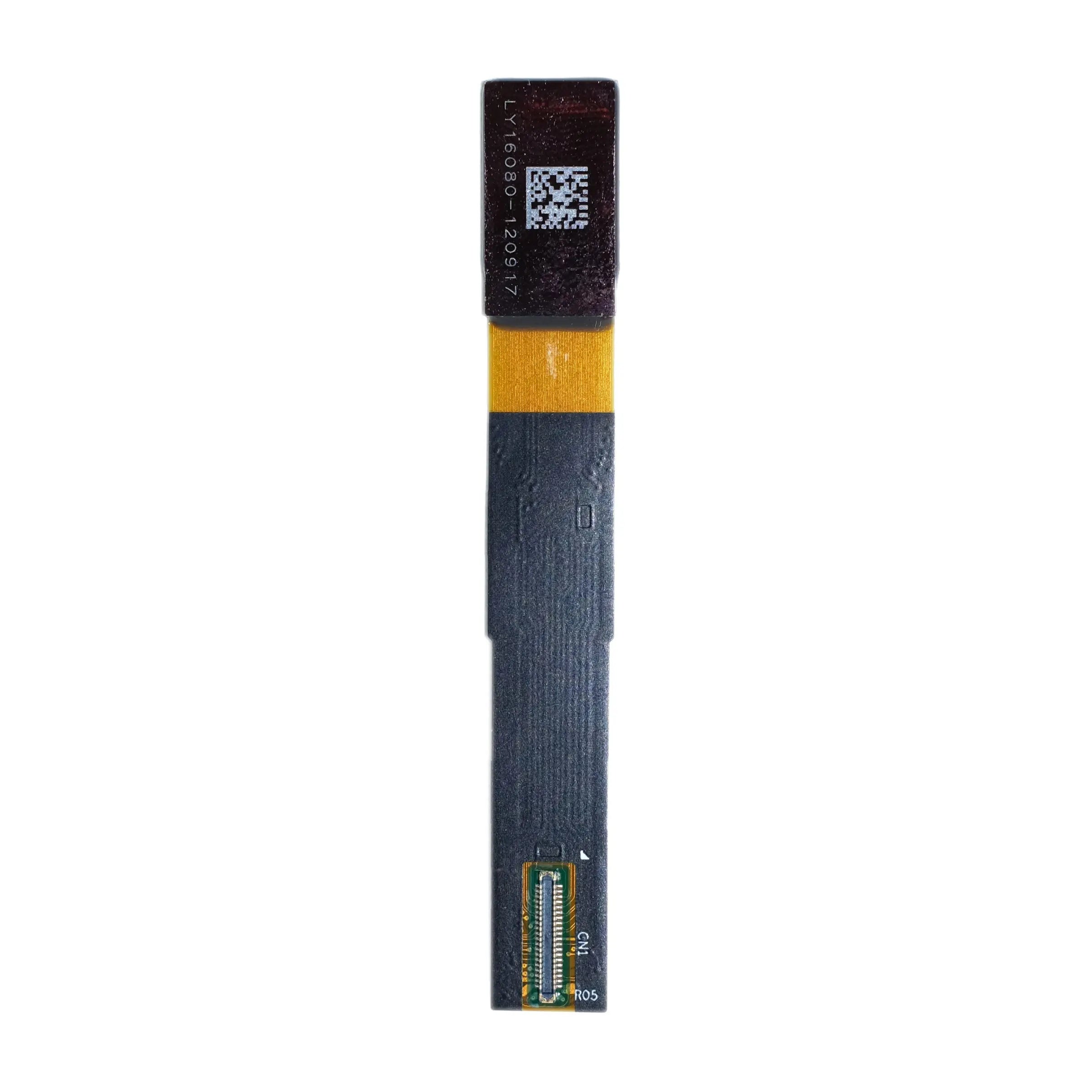
The resulting ultra-thin module thickness of 1.0mm to 1.4mm, combined with standard I2C or SPI interfaces, allows engineers to quickly complete hardware setup with minimal external components within the 0.5-inch to 3-inch display areas of wearable devices like Fitbits or Garmins.
Intuitive Structural Principle
Stacked Like a Sandwich
Viewed in cross-section, the PMOLED structure is extremely flat, with a total effective light-emitting layer thickness of usually less than 500 nanometers.
Detailed Layer Breakdown:
- Anode Layer: The bottom layer is typically Indium Tin Oxide (ITO). This is a transparent conductive material with a light transmission rate required to be above 90% and sheet resistance controlled between 10 to 20 ohms/square.
- Hole Transport Layer (HTL): Located above the anode, with a thickness of about 500 to 1000 Angstroms. Common materials like NPB are used to lower the barrier for hole injection from the anode, helping holes move smoothly to the emission zone.
- Emissive Layer (EML): This is the area where electrons and holes recombine to produce Excitons.
- Electron Transport Layer (ETL): Helps electrons move from the cathode to the emissive layer; a common material is Alq3.
- Cathode Layer: The top metal electrode, typically using low work function metals such as Aluminum (Al), Magnesium-Silver alloy (Mg:Ag), or Calcium (Ca).
Emission at Grid Intersections
The anode is photolithographically patterned into a set of parallel strip conductors (representing data columns), while the cathode is placed as strip conductors perpendicular to the anode (representing scan rows).
- Physical Pixel Definition: A pixel is not an independent component but simply the small rectangular area where the anode strip and cathode strip overlap in space.
- Separator Process: To prevent short circuits during cathode deposition, "mushroom-shaped" cathode separators made of photoresist material are pre-built between anode strips during manufacturing.
Extremely High Instantaneous Current
Since there is no storage capacitor to maintain pixel brightness throughout the frame cycle, PMOLED must utilize "Multiplexing" for driving.
Each row of pixels is lit for only a very short time in each frame.
To ensure the human eye perceives sufficient average brightness, the instantaneous brightness of the pixel at the moment it is lit must be extremely high.
Data Conversion Logic:
Assume a screen with 128 rows (Duty Cycle 1/128) and a target average brightness of 100 nits (cd/m²):
- Instantaneous Brightness Requirement: Theoretically, the brightness at the moment of conduction needs to reach 100 nits x 128 = 12,800 nits. Considering luminous efficiency losses, the actual driving current density usually needs to reach the level of several hundred mA/cm².
- Voltage and Power Consumption: To drive such a large pulse current, PMOLED driving voltage is usually between 7V and 16V, far higher than the 3.3V of logic circuits. This is also why PMOLED power consumption rises sharply when displaying a full white screen.
No Capacitor to Store Charge
In AMOLED, the capacitor next to the TFT stores voltage, allowing the pixel to continue emitting light after the scan line moves away (Hold-type display).
PMOLED, however, lacks this capacitor and belongs to the Impulse-type display category.
Driving Timing Details:
- Scanning Phase: The Driver IC sequentially activates each row (Common). The selected row is pulled low to ground (GND) or a negative voltage.
- Data Injection: Simultaneously, all column (Segment) electrodes source current (Current Source) according to the image data required for that row.
- Off State: When the scan line moves to the next row, the voltage of the previous row returns to a high-impedance state or Reverse Bias voltage.
The table below shows the electrical characteristic differences caused by this capacitor-less structure of PMOLED:
| Characteristic Parameter | PMOLED (Passive) | AMOLED (Active) | Structural Impact |
|---|---|---|---|
| Components per Pixel | Only Organic Layers | 2+ TFTs, 1 Capacitor | Extremely simple structure |
| Emission Mode | Pulsed (Duty Cycle) | Hold Type | Requires high instantaneous current |
| Driving Voltage | 10V - 18V | 4V - 6V (OLED layer) | Main load on boost circuit |
| Response Speed | < 10 microseconds | < 10 microseconds | No difference |
Few External Interfaces Required
Thanks to the intuitiveness of its construction, the PMOLED Driver IC is usually encapsulated directly on the glass substrate (COG, Chip On Glass) or integrated onto the flexible circuit board (COF, Chip On Film).
For the system side, this structure encapsulates the complex matrix scanning tasks entirely within the driver chip. The external MCU only needs to send instructions via a few simple buses:
-
Command Set: Such as
Set Contrast Control(set contrast current),Set Multiplex Ratio(set scan line count). These commands correspond directly to internal current source registers and timing generators. - Video Memory Mapping (GDDRAM): The driver chip features an internal Static RAM (SRAM) that corresponds 1:1 with the screen resolution. The MCU only needs to write data into this RAM, and the driver chip will automatically scan this simple physical grid according to the set duty cycle and refresh rate.
Comparison of Mask Processes
It Takes a Long Time to Make One
Every time a mask step is added, the glass substrate on the production line must undergo at least six to eight physical and chemical steps.
- Cleaning: Removing surface particles.
- Deposition: Sputtering metal or Chemical Vapor Deposition (CVD) of insulating layers.
- Coating: Spin coating Photoresist.
- Exposure: UV light passes through the mask to irradiate the substrate; Stepper machines require extremely high alignment precision.
- Development: Washing away the exposed (or unexposed) photoresist.
- Etching: Wet etching or Dry etching (ICP/RIE) to remove the unprotected film layers.
- Stripping: Removing the remaining photoresist.
- Inspection: AOI optical inspection to find defects.
PMOLED Requires Only a Few Steps
The PMOLED backplane process does not require manufacturing active devices (transistors), only conductors and insulating structures. This compresses its mask requirements to the limit.
The standard PMOLED lithography flow typically involves 4 to 6 masks:
- Anode Patterning (ITO Patterning): First mask. Etching parallel transparent conductive anode strips on the glass substrate.
- Auxiliary Electrode: Optional. If the screen size is slightly larger, a layer of metal bus is added to reduce ITO resistance, requiring one mask.
- Insulator: Second or third mask. Defines the light-emitting area (Opening) of the pixel, covering the edges of the anode to prevent breakdown caused by excessively strong edge electric fields.
-
Cathode Separators: This is a clever design unique to PMOLED, usually requiring one mask. Using negative photoresist to build inverted trapezoidal (mushroom-shaped) microstructures.
- Eliminating Etching: This structure naturally cuts the metal film due to its own shadowing effect during the subsequent cathode metal evaporation, forming independent cathode strips.
The entire process can typically be completed within 3 to 5 days, whereas complex TFT backplanes may take weeks.
TFT is Truly Troublesome
To highlight the simplicity of PMOLED, one must observe the LTPS (Low-Temperature Polysilicon) TFT backplane process required by its competitor, AMOLED.
LTPS is needed to provide sufficient driving current for AMOLED pixels, and its microstructure is extremely complex.
A typical LTPS backplane requires 9 to 13 masks, or even more:
- Light Shield: Prevents light from hitting the transistor and causing leakage.
- Buffer Layer & Semiconductor Layer: Depositing amorphous silicon and laser annealing it into polysilicon.
- Doping: Requires multiple masks to separately define N-type and P-type transistor regions (NMOS/PMOS).
- Gate Insulator & Gate Metal: Defines the electrode controlling the switch.
- Interlayer Dielectric: Drilling Via Holes to connect different levels.
- Source/Drain Metal: Data transmission lines.
- Planarization Layer: Since the bottom layer is too undulating, organic resin needs to be coated and holes drilled.
- Pixel Electrode (Anode): Connects to the OLED material.
- Pixel Definition Layer (PDL): Separates each sub-pixel.
If the via hole position in the 5th mask shifts by 2 microns, it might fail to contact the semiconductor in the 2nd layer, causing the entire panel to be scrapped.
Since PMOLED has fewer layers, the pressure of this Stack-up Tolerance is very low.
Saves Significant Money and Time
The difference in the number of masks directly translates into a huge gap in Non-Recurring Engineering (NRE) costs and Time-to-Market.
NRE Cost Comparison:
- PMOLED: The cost for a set of mask molds is usually between $2,000 and $5,000. For customized small-batch projects (e.g., 10,000 units), the tooling cost amortized over each screen is almost negligible.
- AMOLED / TFT-LCD: The cost for a set of high-precision masks often exceeds $100,000, or even higher.
Yield Calculation Logic:
Assume the single-step yield for each mask process is 98% (0.98).
- PMOLED (5 steps): Total yield is approx $0.98 \times 0.98 \times 0.98 \times 0.98 \times 0.98 \approx 90.4\%$.
- LTPS TFT (11 steps): Total yield is approx $0.98$ to the power of 11 $\approx 80.0\%$.
This 10% yield gap represents a huge loss of profit in mass production.
Fewer process steps allow PMOLED to maintain a high output rate even in less strictly controlled production environments, which is why many old LCD production lines can switch to producing PMOLED with simple retrofitting.
Fast Hardware Integration
Driver Chip Handles Everything
In TFT-LCD systems, an MCU is typically required to provide RGB interfaces (like RGB888 or RGB565) and vertical/horizontal synchronization signals (VSYNC/HSYNC), and may even need specialized LCD controller peripherals and external SDRAM as a Frame Buffer.
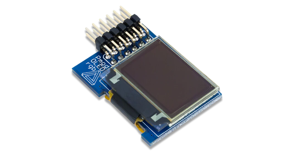
The vast majority of PMOLED screens use COG (Chip On Glass) packaging technology, directly bonding a dedicated Driver IC, such as the industry-standard Solomon Systech SSD1306, SSD1309, or Sino Wealth SH1106.
The internal architecture of these controllers is a complete subsystem:
- Internal GDDRAM: The chip integrates Graphic Display Data RAM that corresponds perfectly to the screen resolution. For a 128 x 64 resolution, the chip comes with at least 1KB (128 x 64 bit / 8) of SRAM internally.
- Internal Oscillator: The chip has a built-in RC oscillation circuit that self-generates the clock signals needed for display, requiring no external crystal input.
- Internal Timing Generator: Automatically generates complex timing waveforms required for row scanning and column driving; the MCU does not need to care about specific microsecond-level scanning rhythms.
Control with Just Two Wires
The simplicity of the interface is the most intuitive advantage of PMOLED hardware integration.
To accommodate IoT node devices or portable medical instruments where pin resources are extremely tight, PMOLED Driver ICs universally support serial communication protocols.
I2C (Inter-Integrated Circuit) Bus Mode:
This is the most pin-saving solution.
- SDA (Serial Data): Data line, bi-directional transmission of commands and image data.
- SCL (Serial Clock): Clock line, synchronizes data transmission.
- Address Selection: Most modules provide an SA0 pin, allowing two PMOLED screens to be mounted on the same bus (addresses are usually 0x3C or 0x3D).
With just 2 GPIO (General Purpose Input/Output) pins from the MCU, or even without a hardware I2C controller (via software Bit-banging), control can be achieved at rates of 100kHz or 400kHz.
This is a lifesaver for ultra-small package MCUs (like QFN20) with fewer than 20 pins.
4-Wire SPI (Serial Peripheral Interface) Mode:
When higher frame rates are needed (e.g., displaying animations), SPI is the first choice.
- CS (Chip Select): Chip select signal.
- CLK (Clock): Clock signal, typically supporting up to 10MHz or higher.
- MOSI (Master Out Slave In): Master output slave input data line.
- D/C (Data/Command): Data/Command selection pin. This is a very efficient design; by flipping the level of this pin, the MCU can instantly switch between sending configuration commands or pixel data, greatly improving protocol efficiency.
In contrast, parallel 8080 or 6800 interfaces, while faster, require 8 data lines plus 4 to 5 control lines, which are increasingly rarely used in modern designs that emphasize miniaturization.
PMOLED's perfect support for serial interfaces reduces PCB Routing difficulty to an absolute minimum.
No External Voltage Boosting Needed
OLED is a current-driven device, and because PMOLED uses row-by-row scanning with high instantaneous brightness, its driving voltage (VCC_OLED) usually requires a high voltage of 7V to 16V.
However, the battery voltage of portable devices is usually only 3.7V (Lithium battery) or even 3.0V (Coin cell).
Traditional solutions involve adding an external Boost Converter chip (like TPS61040), along with an inductor, Schottky diode, and feedback resistors.
This not only increases BOM (Bill of Materials) costs but also occupies valuable PCB area.
PMOLED Driver ICs internally integrate a Charge Pump regulator, cleverly solving this problem.
- Capacitor Boost: Only need to connect 2 ordinary ceramic capacitors (usually 1uF or 2.2uF / 16V) between the pins reserved on the driver IC (e.g., C1P/C1N, C2P/C2N).
- Internal Switching Logic: The chip's internal switching circuit switches the connection of capacitors at high frequency, "transporting" and doubling the input 3.3V low voltage to the required 7V - 14V high voltage.
Software Libraries Ready to Use
The simplicity of the hardware connection has directly spawned a thriving software ecosystem.
Since the register definitions of PMOLED controllers like the SSD1306 have become de facto industry standards, software engineers almost never need to read hundreds of pages of Datasheets to write drivers from scratch.
- Cross-Platform Support: Whether it's Bare-metal code, FreeRTOS, or advanced Linux, Android Things, or even Python (for Raspberry Pi), proven open-source driver libraries can be found.
- Ready-made Graphic Primitives: Common graphics libraries (such as u8g2, Adafruit_GFX) have highly optimized video memory operations for PMOLED. Functions for drawing points, lines, circles, and bitmap fonts are available out of the box.
- Memory Optimization: For MCUs with extremely small memory (e.g., models with less than 1KB RAM), driver libraries usually offer a "Page Buffer" mode. Instead of building a full-screen buffer at once, the screen is divided into several 8-pixel high horizontal strips (Pages), and the MCU calculates and transmits only these 128 bytes of data at a time before processing the next page.
Cost-Effectiveness
PMOLED's high cost-effectiveness stems from its "subtraction" design philosophy: due to its self-emissive nature, it completely removes the backlight module composed of light guide plates, brightness enhancement films, and LED beads, compressing the overall thickness to within 1.5mm.
On the manufacturing end, PMOLED discards complex Thin-Film Transistor (TFT) arrays in favor of a simple anode-cathode cross structure.
This reduces photolithography mask steps by about 20% to 30%, directly lowering equipment depreciation allocation and yield control costs.
For display needs under 3 inches, this technical route provides a highly competitive Bill of Materials (BOM) cost while ensuring high contrast.
Streamlined Manufacturing Process
Structure Like a Sandwich
The basic pixel structure of PMOLED consists of an anode, an organic light-emitting layer, and a cathode.
This structure does not require complex semiconductor processing.
When producing AMOLED, factories must use LTPS (Low-Temperature Polysilicon) or IGZO (Indium Gallium Zinc Oxide) processes to create the backplane.
Taking LTPS as an example, to form transistors with switching functions, a series of lithography processes including cleaning, deposition, coating, exposure, development, etching, and stripping are required.
- TFT Backplane: Typically requires 5 to 9 Mask steps.
- PMOLED Backplane: Requires only 2 to 3 Mask steps. It only needs to etch parallel ITO (Indium Tin Oxide) as anodes on the glass substrate, then create insulating layers and separators.
This difference drastically shortens the production cycle (Takt Time) for PMOLED.
The time it takes for raw glass to enter the production line and emerge as a finished panel is often only half or even shorter for PMOLED compared to TFT-LCD or AMOLED.
Automatic Cathode Separation
In PMOLED manufacturing, there is a very clever and cost-saving process detail called "Cathode Separators" or "Mushroom Head Structure."
After evaporating the organic light-emitting material, an upper metal cathode needs to be created.
If following conventional semiconductor processes, this would require another round of lithography and etching to slice the entire metal layer into parallel lines.
However, in the PMOLED process, engineers pre-fabricate an inverted trapezoidal insulating photoresist structure during the anode production stage.
- Physical Shadowing: When metal aluminum vapor deposits upward from below, this inverted trapezoidal "mushroom head" creates a shadow effect.
- Natural Disconnection: The metal deposited at the bottom of the trench and the metal deposited on top of the insulating layer naturally disconnect, forming independent cathode lines without extra etching steps.
Extremely Low Equipment Depreciation
Building a Gen 6 AMOLED production line typically requires billions of dollars in investment, and these massive equipment costs are ultimately amortized into every screen.
PMOLED has relatively loose requirements for equipment precision:
- Line Width and Spacing: PMOLED pixel pitch is usually between 0.2mm and 0.4mm, far larger than the micron-level precision of retina displays.
- Lithography Machine Generation: This allows factories to use Gen 2 (370mm x 470mm) or Gen 3.5 legacy production lines.
The equipment on these low-generation lines was often purchased 10 years ago or earlier, and their depreciation has long been fully accounted for in financial reports.
Very High Fault Tolerance
For AMOLED, a tiny dust particle landing in the TFT channel can cause a transistor short or open circuit, creating obvious bright or dark spots, often causing the panel to be scrapped.
| Defect Type | AMOLED Consequence | PMOLED Consequence |
|---|---|---|
| Micron-level Dust | Causes TFT failure, entire row/column anomaly | Only affects resistance of a single pixel, usually unnoticeable |
| Uneven Organic Layer | Causes Mura (display non-uniformity), needs circuit compensation | Less impact on passive driving, hard for human eye to detect |
| Alignment Deviation | Causes aperture ratio drop or color mixing | Pixel is larger; deviation of a few microns doesn't affect function |
Even if there is a minor short circuit risk, it can be salvaged by simply cutting the short point via a Laser Repair process.
The repair success rate is far higher than that of complex Active Matrix panels.
This high First Pass Yield directly dilutes the sunk costs caused by individual scraps.
Simple Driver Bonding
After panel manufacturing is complete, the Driver IC needs to be connected. PMOLED usually uses COG (Chip On Glass) process to press the Driver IC directly onto the pins at the edge of the glass.
Since PMOLED is current-driven and does not need to handle high-speed video signals (like 4K video streams), its Pin Map is very simple.
The particle density requirement for Anisotropic Conductive Film (ACF) is not as high as for high-resolution screens.
- ACF Cost: Conventional density ACF can be used, which is cheaper than ultra-fine pitch ACF.
- Inspection Equipment: The post-bonding Automated Optical Inspection (AOI) equipment does not require extremely high-magnification lenses, making inspection faster.
Removal of Backlight Components
Only Glass, No Plastic Plate
Disassemble any STN-LCD module of the same size, and you will find a thick stack of plastics and films stacked beneath the liquid crystal glass.
The thickest piece is usually the Light Guide Plate (LGP), typically made of PMMA (Polymethyl Methacrylate) or PC (Polycarbonate), with a thickness between 0.3mm and 2.0mm.
PMOLED modules do not need this plastic plate at all.
- Mold Fee Zeroed: To distribute light evenly, the surface of the LGP must be covered with precisely designed microstructures (dots or V-cut grooves). For every new screen size or shape, LCD solutions must pay for expensive injection mold tooling or laser dotting programming fees.
- Material Fee Zeroed: Although the unit price of optical-grade PMMA pellets isn't sky-high, with shipment volumes in the millions, the cumulative material cost of this plastic plate is substantial. For small screens like 0.96 inch or 1.3 inch, the LGP often accounts for more than 30% of the total backlight module cost.
Saving Multiple Expensive Brightness Enhancement Films
In traditional LCD structures, light emitted from LED beads enters the light guide plate in a chaotic direction.
To "bend" the light toward the user's eyes and increase brightness, optical films must be stacked on top of the LGP.
Standard architectures typically include three layers:
- Diffuser: Used to cover the dots on the light guide plate.
- Brightness Enhancement Film (BEF/Prism): Usually requires two sheets, one vertical prism and one horizontal prism, to correct the light path.
- Reflector: Pasted at the very bottom to prevent light from leaking to the bottom case.
These films, especially high-end enhancement films (like the DBEF series) from major manufacturers like 3M or Mitsubishi, are very expensive when calculated by area.
PMOLED relies on organic material energy level transitions to emit light, which shoots directly through the glass substrate, naturally achieving a field of view exceeding 160 degrees.
The procurement list does not need to include any diffusers or prism sheets, and inventory management is spared a major category of optical consumables that are extremely sensitive to humidity and static electricity.
No Fear of Dust Ingress During Assembly
Backlight module assembly is a high-incidence area for yield loss in display production. Because LCD glass (Cell) and backlight modules (BLU) are manufactured separately and then laminated, an air layer exists in between.
- Foreign Matter Control: If a single dust particle larger than 0.1mm in diameter falls between the backlight and the glass, an obvious black spot or smudge will be seen when the screen is lit. To prevent this, backlight assembly lines must maintain Class 1000 or even Class 100 cleanliness, and the electricity cost for air filtration systems is a huge hidden expense.
- Newton Ring Elimination: When two smooth planes are too close but not perfectly adhered, light interference produces rainbow-like "Newton Rings." To solve this, LCD assembly often requires adding frame glue or spacer particles to control the gap.
PMOLED is an all-solid-state encapsulation structure.
The organic light-emitting layer is vacuum-evaporated onto the glass, then directly encapsulated using a metal or glass cover with desiccant.
The entire light-emitting area is sealed; there is no gap between a "backlight layer" and a "display layer."
The production line does not need to arrange a large amount of manual Re-work to clean up dust that fell into the backlight, which directly lowers labor costs.
Fewer Components to Solder on the PCB
The chain of cost savings extends to the motherboard (PCBA) design. Driving an LCD backlight usually requires a dedicated boost circuit.
For an edge-lit backlight containing 2 to 4 LED beads, the battery voltage (3.7V) typically needs to be boosted to 9V or 12V to drive the series-connected LED string. The motherboard must accommodate:
- LED Driver IC: Or occupy one channel of the PMIC.
- Power Inductor: Bulky and accounts for a relatively high percentage of price.
- Schottky Diode: To assist boosting.
PMOLED is a voltage-driven device, and many integrated Driver ICs (like SSD1306) already have built-in Charge Pump circuits internally, requiring only two small external capacitors to generate the VCC voltage needed by the panel.
For system engineers, this not only saves the BOM cost of external boost converters but also saves Layout Area on the PCB, which is extremely attractive for space-constrained smart bands or e-cigarette products.
Cheaper Flexible Printed Circuit (FPC)
The FPC connecting the screen to the motherboard is also part of the cost.
- LCD FPC: Usually has a complex structure because it needs to split into two power paths: one for LCD glass logic driving and another large-current line specifically for powering backlight LEDs.
- PMOLED FPC: Pin definitions are very clean. Since no backlight power pins are needed, the FPC typically only requires a single-sided single-layer board to meet requirements, and the number of Gold Fingers is relatively small.
Flexible Custom Development
Change an Icon by Modifying Just One Mask Layer
To understand why PMOLED customization is cheap, one must look at how it "draws" pixels.
For TFT-LCD or AMOLED to change pixel shape or arrangement, the entire Thin-Film Transistor (TFT) array usually needs redesigning.
Modifying 5 to 10 mask layers not only involves a design cycle of several months but the cost for this set of mask molds can easily move in the tens of thousands of dollars.
The pixel shape of PMOLED is determined entirely by the intersection points of the Anode (ITO) and Cathode (Metal).
Especially for those hybrid screens that mainly display fixed icons (Segment type) or icons plus dot matrix (Icon + Dot Matrix):
- Minimal Mask Modification: Usually, modifying just the graphic design of the Anode ITO mask layer is enough to change a square pixel into a heart shape, a battery symbol, or a company logo.
- No Major Changes to Cathode: The upper metal cathode usually maintains a simple strip structure and does not need complex changes to match pixel shapes.
This "single-layer modification" characteristic keeps the NRE fee for PMOLED pattern customization usually within the range of $2,000 to $5,000.
In contrast, the NRE fee for customizing a TFT-LCD panel of the same size typically starts at $20,000 to $50,000, and costs multiply if irregular cutting (like circular or notched shapes) is involved.
Free-form Cutting without Heartache
Current smart hardware increasingly pursues unique shapes; demand for circular, bar-shaped, or even trapezoidal screens has surged.
In the TFT-LCD field, Free-form cutting is a high-risk process.
Because LCDs sandwich liquid crystals between two layers of glass, complex Sealing processes are required after cutting to prevent leakage, and cutting edges are prone to stress leading to TFT line breaks.
This leads to extremely low yields and skyrocketing unit prices.
PMOLED is a solid-state structure and does not rely on perimeter sealant to maintain function.
- High Cutting Freedom: Glass substrates can be scribed and cut before or after evaporation. Since there is no liquid substance, there is no worry about internal materials flowing out.
- Simple Encapsulation: Even for circular PMOLEDs, the encapsulation Cap can use standard circular glass, cured with UV glue, with process difficulty similar to rectangular screens.
- Flexible Wiring Layout: The PMOLED driver chip is usually bonded on one side of the glass. For applications like ring-shaped bands, the FPC bonding area can be designed on any side of the screen, or the FPC pins can be hidden directly under the display area via shaped glass, achieving a true "bezel-less" visual effect.
Very Low MOQ Threshold
In supply chain management, Minimum Order Quantity (MOQ) is often the last straw that breaks a startup.
To maintain utilization rates for Gen 6 or Gen 8.5 lines, large panel makers usually require monthly orders for a single model to reach 50k or 100k units before accepting an order.
PMOLED manufacturers mainly use smaller Gen 2.5 or Gen 3.5 lines.
- Substrate Utilization: A single 370mm x 470mm Gen 2 substrate, if cut into 0.96-inch screens, can yield several hundred pieces.
- Fast Switchover: Another advantage of small production lines is short Changeover time. Switching from producing medical screens for Customer A to e-cigarette screens for Customer B might only take a few hours to change masks and clean chambers.
Therefore, PMOLED suppliers can usually accept Pilot Run orders of 1k (1,000 pieces) or even 500 pieces, and MOQs after mass production often stay at the level of 3k to 5k pieces.
Pick Colors Freely
Unlike LCDs which rely on backlight LED colors or Color Filters, PMOLED colors depend on the organic Emitter material itself.
- Rich Material Selection: There are mature blue, yellow, white, amber, green, and even red OLED materials on the market.
- Area Color: On a single screen, yellow organic material can be evaporated on the top half (for status bars) and blue organic material on the bottom half (for content). This does not require expensive Fine Metal Masks (FMM) to implement RGB pixel arrangement, but only requires simple metal baffles for zonal shielding during evaporation.
Performance
In the field of small-sized displays under 3 inches, PMOLED offers a contrast ratio exceeding 10,000:1, with black pixels emitting absolutely no light, achieving a true pure black background.
Its response speed is as fast as 10 microseconds (<0.01 ms), more than 1000 times faster than ordinary LCDs, completely eliminating ghosting in scrolling text or dynamic icons.
Furthermore, it can work normally in extreme cold environments of -40°C without heating and supports a wide viewing angle of 175 degrees, close to flat, making it the preferred solution for industrial meters and outdoor portable equipment.
Pure Black Contrast Presentation
Pixel Self-Emission Mechanism
To understand PMOLED's high contrast, one must look at its internal charge carrier injection process. The PMOLED structure consists of a matrix formed by crossing anode and cathode strips.
- Emissive Layer (EML) is sandwiched between the anode and cathode.
- Only when voltage is applied to specific row and column intersections do electrons and holes combine in the organic layer to release photons.
- Unselected pixels or pixels with zero voltage remain in an electrochemically dormant state, producing zero photons.
In contrast, STN-LCD or TN-LCD backlights remain constantly on even when displaying a full black screen.
Although liquid crystal molecules twist to block light, they cannot achieve 100% shading.
Typically, 0.1 to 0.5 cd/m² of light leaks through the filters, causing the original black background to look dark gray or glow blue in a dark room.
This noise brightness limits LCD maximum contrast to typically around 500:1, while PMOLED easily reaches 10,000:1 or even higher.
Character Edge Clarity
In common PMOLED sizes like 0.96 inches or 1.3 inches, resolutions are typically 128x64 or 128x32. Due to limited pixel density, the expressiveness of every pixel is crucial.
- Zero Blooming Effect: On LCD screens, black pixels surrounding a bright pixel may glow slightly due to backlight scattering, causing blurred text edges (Blooming).
- Pixel Isolation: PMOLED pixels are physically separated by insulating layers (Polyimide banks). A white pixel with 200 nits brightness can be immediately adjacent to a black pixel with 0 nits brightness.
This extreme juxtaposition of light and dark makes tiny characters of 6x8 or 8x16 dot matrix exceptionally sharp.
When industrial instruments display values or wearable devices show heart rate numbers, users don't need to squint to separate effective information from the background.
| Display Technology | Black Brightness (cd/m²) | Typical Contrast | Inter-Pixel Light Interference |
|---|---|---|---|
| TN-LCD | > 0.40 | 300:1 | High (Backlight scattering) |
| STN-LCD | > 0.20 | 500:1 | Medium (Optical crosstalk) |
| PMOLED | 0.00 | > 10,000:1 | None |
Black Doesn't Turn Grey from the Side
LCD contrast is directional.
Due to the birefringence of liquid crystal molecules, when a user's line of sight deviates from the vertical normal (e.g., viewing from a 45-degree angle), the liquid crystal molecules that originally blocked light cannot effectively shade it.
Black areas rapidly turn gray, or even suffer color inversion, causing contrast to drop sharply below 10:1.
The PMOLED emissive layer acts as an approximate Lambertian Emitter, radiating light uniformly into the hemispherical space.
- Viewing Angle Maintenance: At extreme angles of 160 degrees or even 175 degrees, black pixels remain in a non-emitting state.
- Contrast Attenuation: Even at large angles, contrast can still be maintained above 1,000:1.
For screens installed on the side of control panels, auxiliary displays on car center consoles, or medical probes, regardless of where the operator stands, the screen background always blends with the device bezel, avoiding the appearance of a gray rectangular patch.
Scan Cycle and Brightness
PMOLED operates using row-by-row scanning (Duty Driving). For the human eye to perceive sufficient brightness, lit pixels must have very high instantaneous brightness during their extremely short conduction time.
- Duty Cycle: Typically 1/64 or 1/128.
- Instantaneous Brightness: To achieve an average brightness of 100 nits, the brightness of the pixel at the moment of conduction may be as high as 6,000 nits or more.
This high-intensity pulsed light emission further enhances the human eye's perception of contrast.
Although high voltage driving (typically 12V - 16V) brings power consumption challenges, for black pixels, the current remains zero regardless of how high the driving voltage is on the scan line for inactive pixels.
Ambient Light and Contrast
In indoor or low-light environments, PMOLED's pure black performance is dominant.
However, in strong light environments (like direct outdoor sunlight), reflections from the screen surface can affect contrast.
To maintain the "Pure Black Contrast Presentation" effect, PMOLED modules are usually used in conjunction with a Circular Polarizer.
- Principle: Ambient light enters the screen and becomes linearly polarized light after passing through the polarizer. After reflecting off the internal metal electrodes, the polarization direction rotates 90 degrees, thus being blocked by the polarizer and unable to exit.
- Result: Even under sunlight, the non-emitting areas of the screen appear deep black rather than the metallic color of electrode reflections.
With a circular polarizer, although overall transmission drops to around 42% - 45%, given PMOLED's natively high contrast, this brightness loss is worthwhile as it ensures background blackness meets standards under various lighting conditions, maintaining data readability.
Microsecond Response Speed
Electrons Run Faster than Molecules
To quantify PMOLED's speed advantage, one must compare the "Rise Time" (dark to bright) and "Fall Time" (bright to dark) of both technologies.
LCD panels (especially STN or TN types) require liquid crystal molecules to realign their orientation within a viscous fluid after voltage is applied; this process involves the movement of physical mass.
- LCD Typical Response: Rise time is about 10 ms, Fall time may exceed 20 ms, totaling about 30 ms.
- PMOLED Typical Response: Electrons and holes have extremely high mobility under an electric field, and recombination emission is almost instantaneous. Rise and Fall times are both less than 10 microseconds (0.01 ms).
With this 3000-fold speed difference, the switching action of PMOLED pixels is almost synchronized with the driving signal, with no lag.
Observed on an oscilloscope, the optical response waveform of PMOLED is an almost vertical square wave, while LCD is a slowly climbing and descending slope.
Scanning Frequency Keeps Up
PMOLED uses Passive Matrix driving, where each row of pixels on the screen is not continuously lit but scanned row-by-row through rapid polling.
Assume a PMOLED screen with 128x64 resolution, using a 1/64 Duty Cycle and a refresh rate of 100Hz.
- Single Frame Time: 10 milliseconds.
- Single Row Lit Time: 10 milliseconds / 64 rows = 156 microseconds.
Under this high multiplexing drive, the time window for each row of pixels to be selected is extremely brief.
If using millisecond-response LCD materials, the pixel wouldn't even have time to fully brighten before the scan signal moves to the next row, resulting in extremely low brightness and failure to display.
PMOLED's <10 microsecond response speed allows it to easily adapt to 1/128 or even higher duty cycle driving.
Pixels can instantly reach peak brightness under extremely short pulse currents and extinguish instantly after scanning ends, ensuring the feasibility of passive driving schemes at high resolutions.
Instant Reaction Even in Winter
Temperature is a physical variable affecting display response speed. The liquid crystal material inside an LCD is a complex mixed fluid whose Viscosity is very sensitive to temperature.
- Room Temp (25°C): LCD performs normally.
- Low Temp (-20°C): Liquid crystal becomes as viscous as honey, and physical rotation resistance increases dramatically. Response time deteriorates from 30 ms to 500 ms or even seconds.
Even in extreme cold environments of -40°C, PMOLED response speed remains at the microsecond level.
This is critical for display equipment installed on ski goggles, outdoor weather stations, cold chain logistics monitors, or car dashboards, as they do not need to be equipped with high-energy-consuming resistance heating pads like LCDs to maintain screen reaction speed.
| Temperature Condition | STN-LCD Response Time | PMOLED Response Time | Visual Perception |
|---|---|---|---|
| +25°C | ~ 200 ms | < 0.01 ms | LCD has slight ghosting, PMOLED is sharp |
| 0°C | ~ 500 ms | < 0.01 ms | LCD has obvious trailing, PMOLED remains consistent |
| -20°C | > 1000 ms | < 0.02 ms | LCD image freezes, PMOLED is fluid as usual |
Scrolling Text Doesn't Blur
In small-screen applications, due to limited display area, "marquees" or scrolling text are often used to show longer information (like long song titles, SMS notifications, system error messages).
When text moves horizontally across the screen quickly, the human eye tracks the moving object.
- Blur Generation: If pixels do not extinguish fast enough, the afterimage of the old position superimposes on the image of the new position, causing text strokes to thicken and edges to blur, looking like a moving cloud of fog.
- PMOLED Performance: Thanks to extremely short Fall Time, when text moves away from a pixel, that point can instantly turn completely black. Pixel state switching is crisp, without any "afterglow."
Test data shows that at a scrolling speed of 300 pixels per second, English characters displayed on PMOLED remain sharp-edged with extremely high Motion Clarity.
This characteristic makes PMOLED very suitable for MP3 players, smart bands, and alarm scrolling bars on industrial equipment.
Wide Temperature Operation Capability
Lighting Up at -40 Degrees
Liquid crystal materials undergo physical phase transitions at low temperatures, gradually transforming from the anisotropic Nematic phase to the Smectic phase or even crystalline.
- Viscosity Surge: As temperature drops, the rotational viscosity of liquid crystal rises exponentially. At -20°C, LCD response time stretches from 20 ms at room temperature to over 500 ms.
- Freezing Phenomenon: At -30°C or -40°C, the liquid crystal in ordinary STN-LCDs may completely freeze, causing the screen to fail to refresh or present a permanent black/white screen state until the temperature rises.
PMOLED contains no liquid inside. The Electron Mobility through the solid organic layer is minimally affected by low temperatures.
Even in an environment of -40°C, PMOLED maintains a pixel switching speed of around 10 microseconds.
PMOLED screens installed on polar expedition equipment or cold chain logistics recorders display immediately upon startup without any warm-up process, and scrolling is smooth, avoiding the "slowly brightening" or "heavy ghosting" phenomena common with LCDs.
Eliminating Heating Patches
Since LCD performance degrades severely at low temperatures, to ensure normal use in cold regions, system design engineers usually must add a resistive Heater behind the LCD module.
- Energy Burden: The heater consumes a large amount of power to keep the liquid crystal layer temperature above 0°C, which is unacceptable for battery-powered portable devices.
- Structural Thickness: The heating component increases the overall thickness and assembly complexity of the module.
Choosing PMOLED completely eliminates this component.
Device manufacturers do not need to design temperature control circuits to monitor ambient temperature and trigger heating, nor do they need to reserve extra battery budget for the display.
This directly reduces BOM costs and simplifies internal structural design, allowing the final product to be lighter, thinner, and more compact.
No Black Screen or Crashing at High Temperatures
At the high-temperature end, PMOLED also demonstrates physical stability superior to LCD.
Liquid crystal materials have a specific physical parameter called the "Clearing Point" or "N-I Point."
When the ambient temperature exceeds this critical value (typically around +80°C for industrial LCDs), the liquid crystal material loses its liquid crystalline state and becomes an isotropic ordinary liquid.
- LCD Failure: Once it becomes ordinary liquid, the molecules lose their optical rotation ability, and the screen usually turns completely black (in Normally White mode) or completely white, unable to display content at all, colloquially known as "Blackout."
PMOLED organic light-emitting materials have a relatively high Glass Transition Temperature (Tg), usually above 100°C.
In environmental tests at +85°C, PMOLED pixels can still emit light controllably.
Although high temperatures accelerate the aging and decay of organic materials, under short-term extreme high-temperature exposure, PMOLED will not experience sudden physical failure or black screens, ensuring that critical information can be continuously read.
Very Stable Driving Voltage
Temperature changes alter material resistivity and turn-on voltage characteristics.
- LCD Voltage Drift: LCD Threshold Voltage (Vth) varies greatly with temperature (temperature coefficient typically around -0.2% / °C). To maintain consistent contrast across a wide temperature range, LCD drivers must have complex Temperature Compensation circuits, otherwise images become faint and illegible at low temperatures, or "ghosting" and background blackening occur at high temperatures.
Although the resistance of organic materials fluctuates at different temperatures, Driver ICs mainly control brightness via Constant Current Sources.
In the range of -40°C to +85°C, the Forward Voltage (Vf) change of PMOLED is relatively flat and linear.
Modern PMOLED Driver ICs with integrated temperature sensors can easily fine-tune the driving voltage via a simple Look-up Table, ensuring that screen brightness deviation is controlled within 10% across the entire temperature range, and contrast is always maintained at a high level of over 2000:1, with users perceiving almost no visual difference.
| Temperature Environment | LCD Status | PMOLED Status | Compensation Requirement |
|---|---|---|---|
| -40°C | Frozen / Extremely Slow / Very Low Contrast | Rapid Response / Normal Brightness | LCD needs external heating |
| +25°C | Normal | Normal | None |
| +85°C | Turns Black (Enters Isotropic State) | Works Normally | LCD needs protection from direct sunlight |
| Voltage Regulation | Requires significant Vop adjustment | Fine-tuning or Constant Current Auto-adaptation | PMOLED algorithm is simpler |
Wider Storage Range
Besides Operating Temperature, Storage Temperature is also an important indicator for evaluating device reliability.
The typical storage temperature range for PMOLED modules can reach -40°C to +90°C, with some military-grade products even rated up to +105°C.
In Thermal Shock Tests in reliability labs, samples need to switch rapidly between -40°C and +85°C extreme temperature chambers for over 100 cycles.
Due to the simple layer structure of PMOLED, the coefficient of thermal expansion matching between layers is good, and internal circuit breaks or encapsulation glass shattering caused by thermal expansion and contraction rarely occur.
In comparison, the Sealant and Cell Gap of LCDs are more prone to stress failure under drastic temperature changes, leading to leakage or rainbow patterns.
Weiterlesen
It is recommended to purchase modules under 3 inches with a resolution of 128×64. Use 4-pin I2C when I/O is limited, and select SPI for high-speed requirements. Make sure to confirm that brightness...

Manufacturing requires the use of vacuum thermal evaporation technology to deposit an organic material layer with a total thickness of approximately 150 nanometers on the ITO anode. It achieves pro...
Hinterlasse einen Kommentar
Diese Website ist durch hCaptcha geschützt und es gelten die allgemeinen Geschäftsbedingungen und Datenschutzbestimmungen von hCaptcha.