


What is a shaped OLED screen
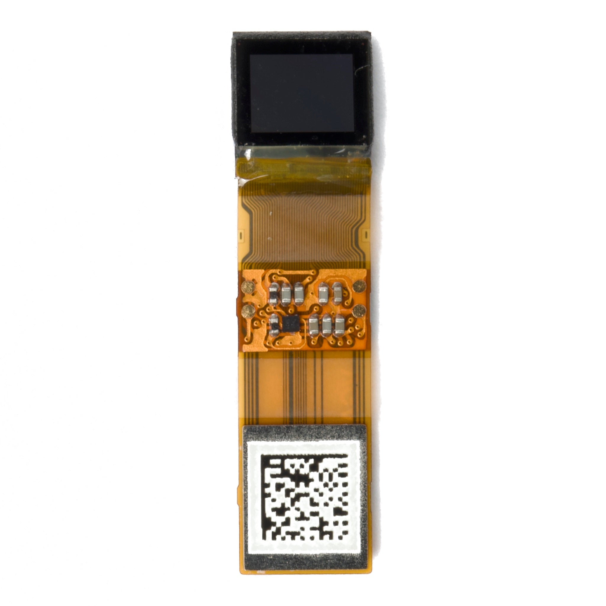
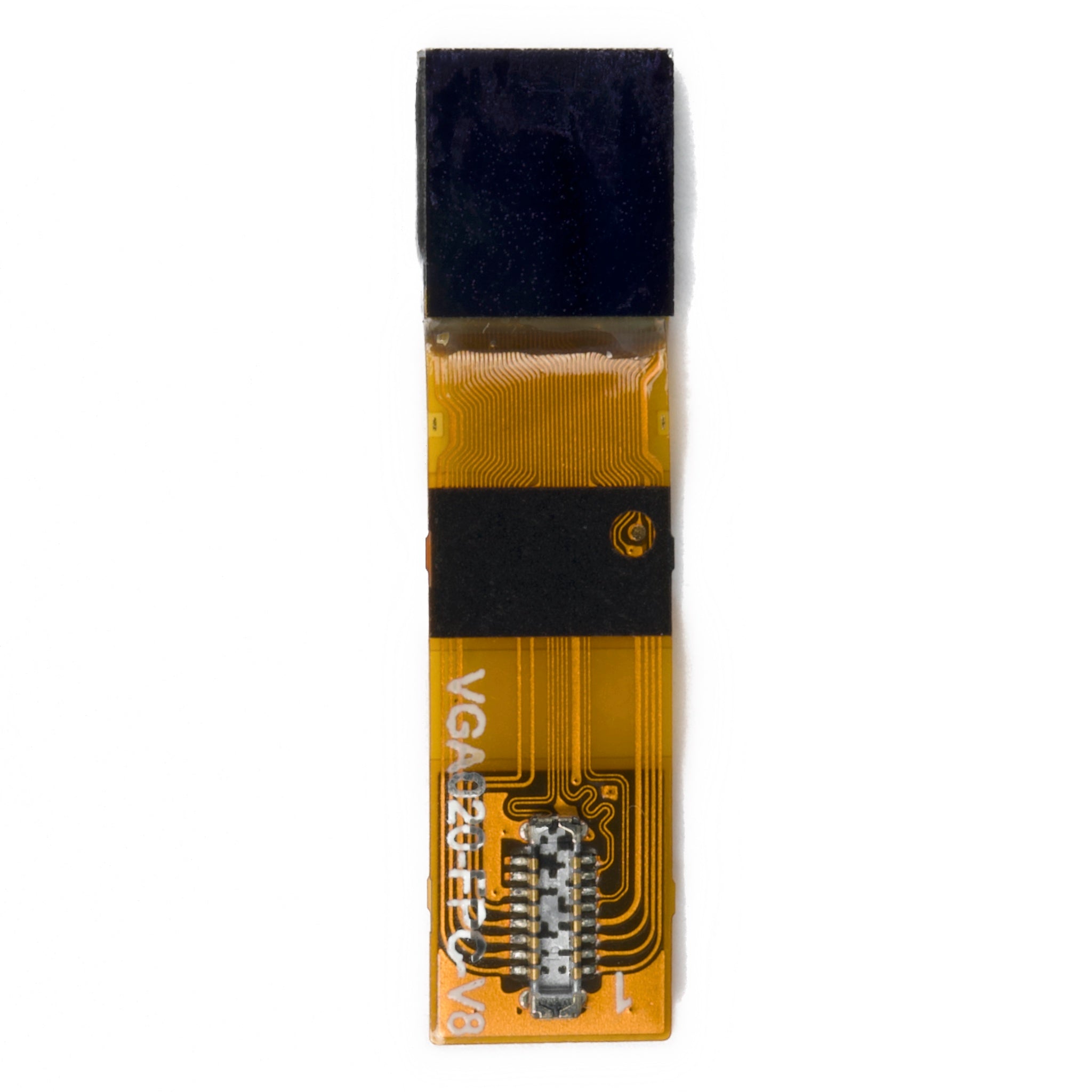
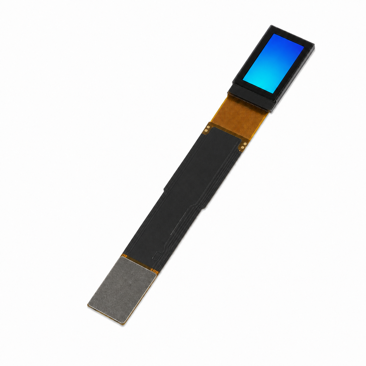
A shaped OLED screen is an OLED display built to a non-rectangular outline or a fixed curvature: circular, rounded, tapered, notched, or bent around a defined radius. The light-emitting stack is the same one used in flat OLED panels. What changes is the substrate it sits on, the line it is cut along, and the mechanical stack that holds it in shape. The display follows the product instead of the product wrapping itself around a rectangle.
Two routes to a shape
Most projects mix two techniques, and they carry different constraints. Shaping in two dimensions means cutting a flat panel to a custom outline: a circle for a watch, a rounded rectangle for a handheld, a panel with a notch or an inner cut-out for a control cluster. Shaping in three dimensions means bending the panel to a fixed radius, either permanently during assembly or repeatedly in a foldable product.
The first is a cutting problem, the second a mechanical one, and suppliers answer them with different yield models.
Why the emitter decides what is possible
An LCD modulates light from a backlight, so the panel is a sandwich of two substrates with a liquid crystal layer of controlled thickness between them. Bending that sandwich changes the cell gap, and a cell gap that varies across the panel shows up as uneven brightness. Curved LCDs exist, usually with thin glass and a single permanent curvature, but the process window is narrow and the part is not intended to be flexed again.
An OLED pixel emits its own light. There is no backlight cavity and no second substrate holding a cell gap, so the stack can be deposited on a plastic substrate and bent afterwards [2]. That is the physical reason shaped displays are usually OLED rather than LCD.
Inside a flexible stack
Fabrication starts by coating polyimide on a carrier glass and building the backplane and OLED layers on top with conventional deposition and lithography. A thin-film encapsulation replaces the rigid cover glass: inorganic and organic layers alternate to block moisture and oxygen, which degrade the organic emitter over time.
Only at the end is the polyimide released from the carrier, typically with a laser. Everything after that step, including cutting, driver bonding, polariser lamination, and cover assembly, has to be done with the panel already flexible. Handling and yield at those steps dominate the cost of a shaped part far more than the deposition itself.
Bending radius belongs to the stack
Bending stress is lowest at the neutral axis, an imaginary surface inside the stack where tension on one side balances compression on the other. If the emissive layer sits at that axis, the pixel barely feels the bend. If it sits away from it, the layer is stretched, and the encapsulation develops micro-cracks that later become moisture paths and dark spots.
Two practical consequences follow. Bending inward, so the emissive side is in compression, is more forgiving than bending outward. And the smallest usable radius depends on total stack thickness, the modulus of each layer, and where the neutral axis falls, not on a single figure quoted for the panel alone. A supplier's radius number is only meaningful with the bend direction and the number of cycles attached to it.
Cutting a custom outline
Laser cutting replaced mechanical scribing for shaped panels because it produces a cleaner edge with fewer micro-cracks and can follow a curve. The cut still costs design freedom in three ways.
The edge needs a border. Gate and source driver circuitry, the power supply ring, and the seal around the encapsulation all live near the perimeter, so the visible area has to be inset from the outline. A tight corner radius concentrates stress and reduces the usable border, which is why very small radii usually come with a larger bezel.
Inner cut-outs break routing. A hole or a notch severs the wires that would otherwise pass through that region, so the driver layout has to route around it and the driver IC may move to a less convenient edge.
Nesting wastes substrate. Rectangular panels tile a mother glass efficiently. Circles and irregular outlines leave unused area between parts, and that scrap is priced into the unit cost before a single panel is built.

Rules worth settling before the drawing is frozen
Five items cause most rework, and all can be agreed before tooling is cut.
- Define the active area and the outline as two dimensions on one drawing, with the minimum border the supplier can actually hold.
- Fix the bend direction and keep it single. An S-curve or a reverse bend loads the same region in both tension and compression and shortens life.
- Keep the flex tail out of the bend zone. A ribbon crossing a curved edge is a fatigue failure waiting for a shipping carton to happen.
- Specify the cover glass and the bonding method together with the panel. Curved lamination needs an optically clear adhesive or resin, and the edge is where bubbles and delamination appear first.
- Approve the cut file and the polariser outline as one drawing. A circular polariser cut to a rounded rectangle leaves a bright sliver at the corner that no firmware can hide.
Where the shape earns its cost
Wearables are the clearest case. A circular watch face only reads as circular if the display is circular, and a rectangular panel behind a round bezel wastes corner area and shows the aperture at every angle. Our round screen modules exist for exactly this reason. Automotive clusters and centre stacks use curvature to keep the screen closer to normal to the driver's line of sight across a wide dashboard, and shaped outlines to fit behind trim without a visible frame.
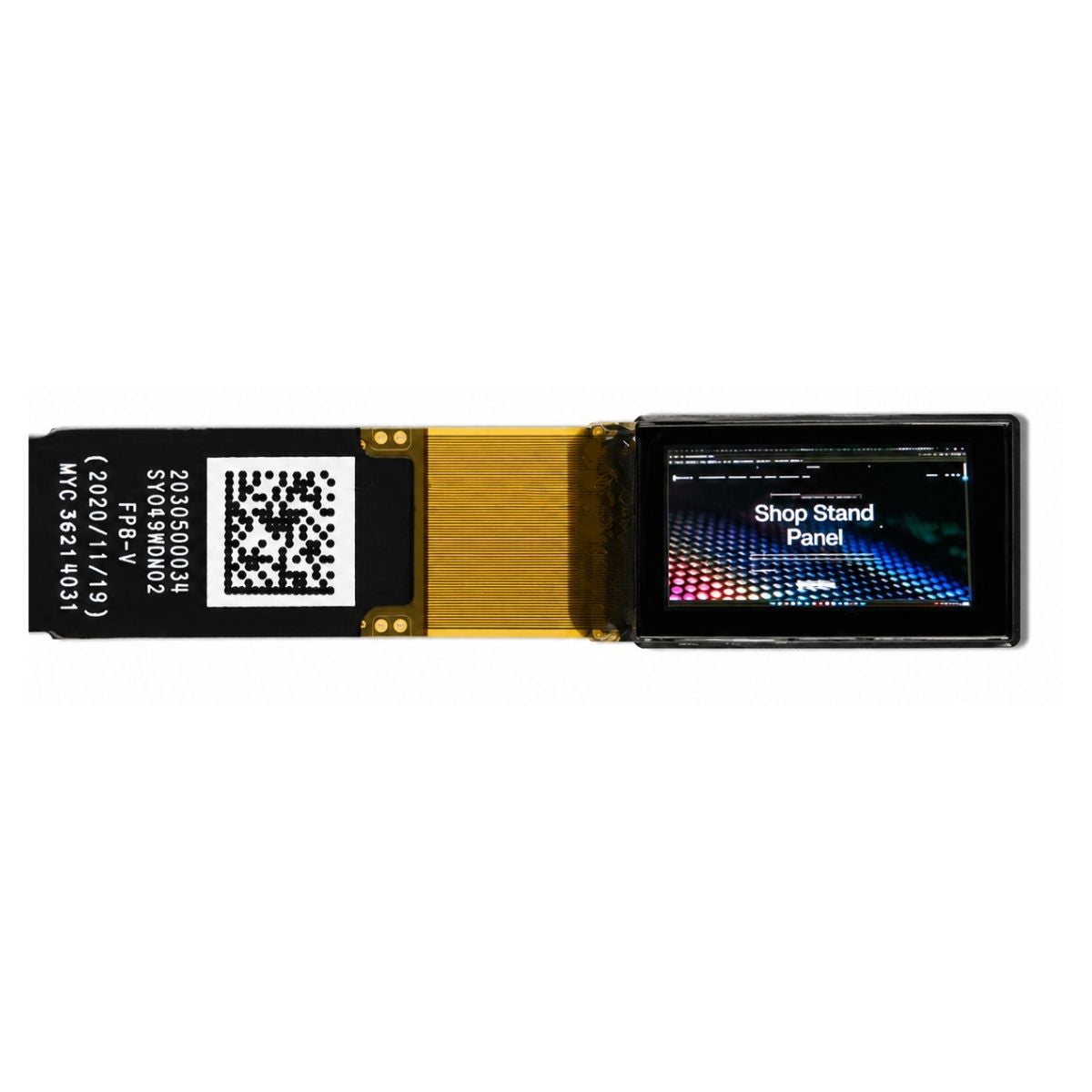
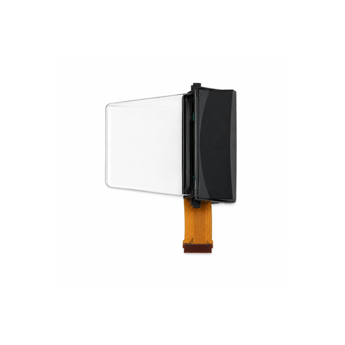
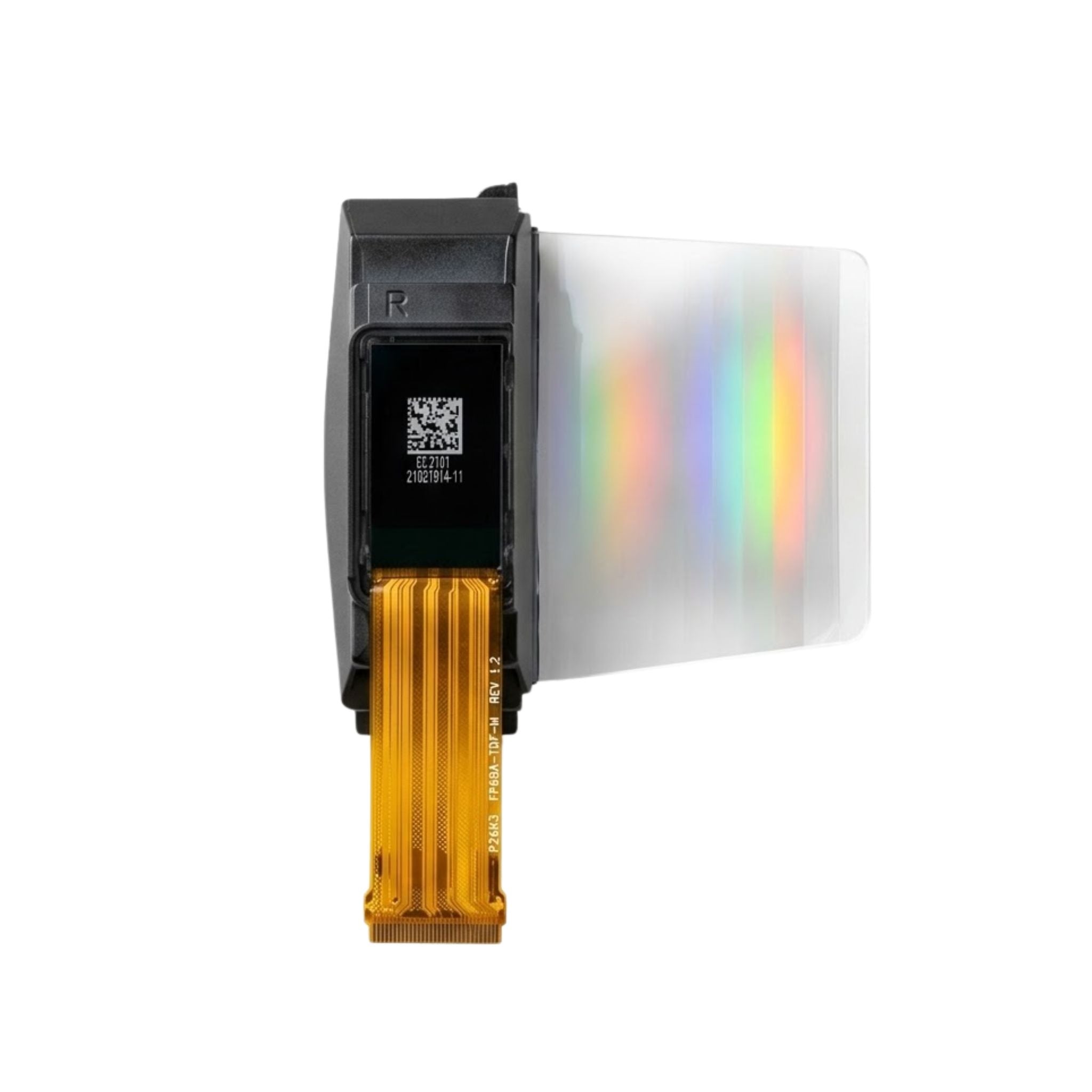
Industrial control panels use cut-outs so a display can sit around physical switches, connectors, or a meter movement instead of forcing a larger enclosure, which is why shaped parts turn up so often in industrial display designs. Near-eye optics in AR and VR use small curved or circular micro-OLED panels because the eyepiece is round and the field of view is angular rather than rectangular.
In each case the shape is functional before it is decorative: it removes a bezel, a clearance, or an optical compromise a rectangle would impose.
Costs that stay out of the unit price
Tooling is per shape. A cut program, a lamination fixture, a test jig, and often a custom flex are not shared with the rectangular version of the same panel, so they do not amortise across a product family the way a standard part does.
Emissive lifetime is harder to manage on a small, dense, shaped panel because the drive current is concentrated in a small area and heat has less room to spread. Blue sub-pixels age fastest, so shaped panels normally ship with pixel compensation that raises drive levels as the emitter dims. Without it, a static interface element such as a clock or a status bar will leave a visible mark within the product's life.
Optical measurement also needs rethinking. Standard display measurement practice, as described in ISO 9241-307, defines measurement points on a rectangular grid [1]. On a circular or notched panel some of those points fall outside the active area, so the test plan has to define its own points and state the luminance and white point at which the readings were taken.
What to send a supplier
A quotation is only comparable if every supplier answers the same question. Send one package: the outline drawing with radii, the active area and the required border; the bend radius, direction and cycle count if the part will be flexed in use; the interface, the driver location and the flex exit side; the cover glass, touch stack and bonding method; and the operating temperature range with the brightness target and the conditions under which it will be measured. If the project is still choosing between emissive and backlit technology, start from the OLED module range before the outline is drawn.
The shape is a system decision, not a drawing decision. Substrate, encapsulation, cut line, neutral axis, and border move together, and the cheapest way to keep a shaped project on schedule is to fix those five before the tooling is cut.
References
- ISO 9241-307:2008 — Ergonomics of human-system interaction — Part 307: Analysis and compliance test methods for electronic visual displays. International Organization for Standardization. https://www.iso.org/standard/40102.html
- Hilsum, C. (2010). Flat-panel electronic displays: a triumph of physics, chemistry and engineering. Philosophical Transactions of the Royal Society A, 368(1914), 1027–1082. https://doi.org/10.1098/rsta.2009.0247
Weiterlesen

Choosing Micro OLED for VR headsets offers 4K-per-eye resolution (sharper than standard LCDs’ ~2K), a 1,000,000:1 contrast ratio (vibrant blacks/whites).

A COG (Chip on Glass) LCD display integrates driver ICs directly onto the glass substrate of the panel, minimizing external wiring; common in compact.
Hinterlasse einen Kommentar
Diese Website ist durch hCaptcha geschützt und es gelten die allgemeinen Geschäftsbedingungen und Datenschutzbestimmungen von hCaptcha.