



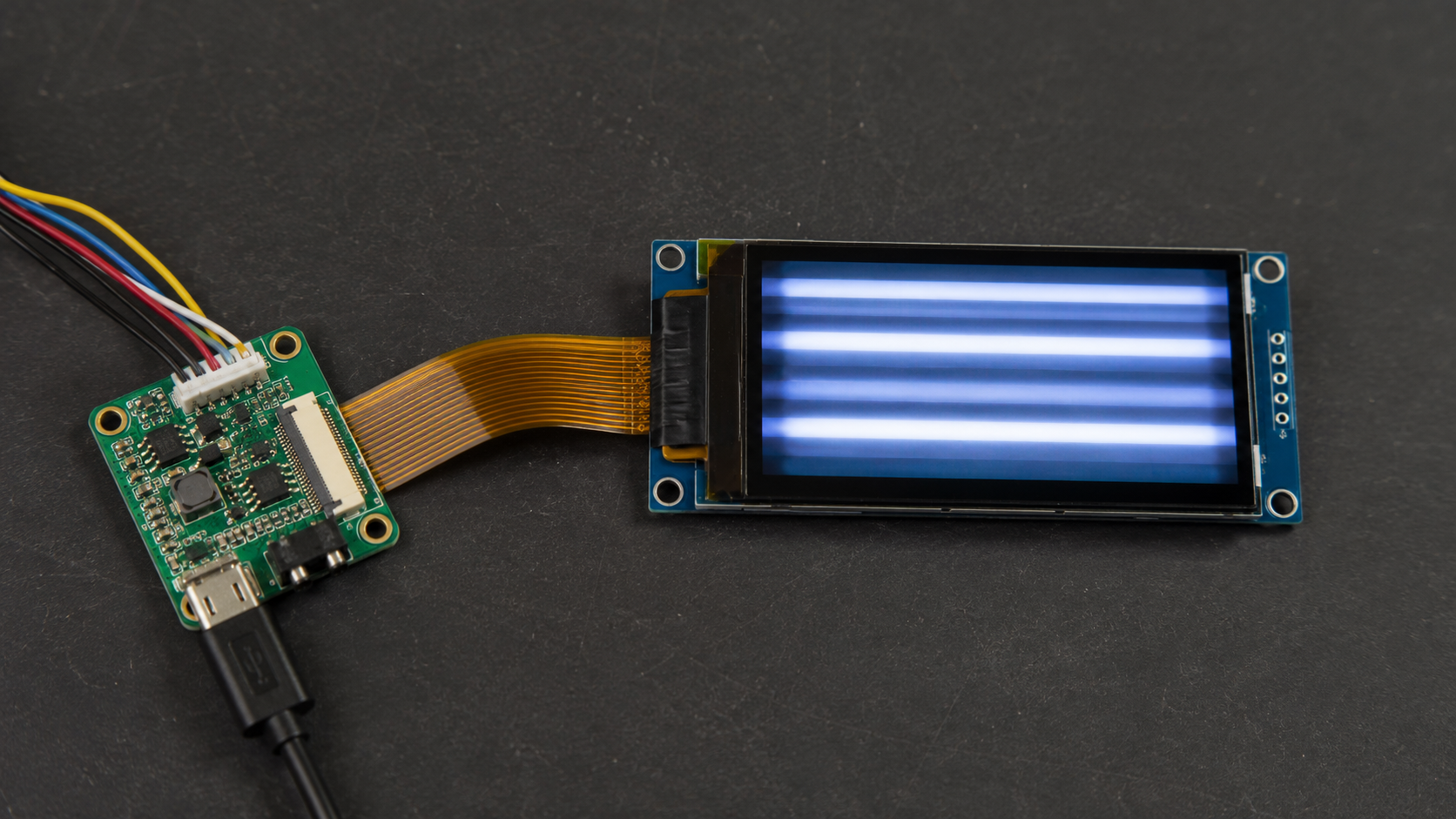
A PMOLED display has uneven row brightness when one physical row receives less current, less effective lighting time, or more voltage loss than the other rows. Common causes include incorrect scan settings, an unstable OLED power rail, a weak COM connection, high row resistance, a damaged driver output, heat, or OLED aging.
A horizontal dark band is not always a panel fault. An eight-pixel-high band may come from one missing display-memory page, while moving bands seen only through a camera may be caused by the camera shutter. First check whether the defect stays at the same position on the glass or follows the displayed image.

How Row Scanning Works
A PMOLED panel is driven one row at a time. COM lines normally select the physical rows, while SEG lines control which columns light in the selected row. The controller scans all rows repeatedly to build a complete image.
On a 64-row panel, the theoretical time available for one row changes with the frame rate:
| Frame rate | Frame time | Theoretical time per row |
|---|---|---|
| 80 Hz | 12.5 ms | About 195.3 μs |
| 100 Hz | 10 ms | About 156.3 μs |
| 120 Hz | 8.33 ms | About 130.2 μs |
These are calculation examples, not fixed PMOLED settings. The useful lighting time is shorter because part of each row period is used for discharge, pre-charge, and signal switching.
If one row has a weak connection or extra resistance, it may need more time to reach the intended current. At a higher frame rate, the shorter row period can make that weak row look darker.
Average brightness mainly depends on:
- The peak current delivered to the pixel.
- The useful emission time during each row period.
- The multiplex duty ratio.
- The efficiency and age of the OLED material.
- The voltage margin available to the driver.
A higher frame rate does not automatically make a PMOLED brighter or darker. It matters when the shorter row period leaves too little time for pre-charge or current settling. A more detailed explanation is available in this guide to how PMOLED row and column driving works.
Know Which Row Is Wrong
Three different parts of the display may be described as a row:
- Logical row: A row in the image created by the software.
- Physical row: A real COM conductor on the OLED glass.
- Memory page: A group of pixel bits stored together in the controller.
An SSD1306-controlled 128×64 display contains 8,192 monochrome pixels:
128 columns × 64 rows = 8,192 pixels
Because each pixel needs one bit, a complete frame needs 8,192 bits, or 1,024 bytes:
8,192 bits ÷ 8 = 1,024 bytes
The SSD1306 divides this memory into eight pages. Each page contains 128 bytes and spans eight vertical COM rows. One byte controls eight vertically arranged pixels in one column.
- 8 pages × 128 bytes = 1,024 bytes
- 1 page = 8 vertical pixel rows
This gives useful fault clues:
- A one-pixel-high fixed line is more likely to involve one physical COM path.
- An eight-pixel-high band is more likely to involve one memory page or data transfer.
- A half-screen fault is more likely to involve mapping, grouped connections, or power distribution.
Not every 128×64 OLED uses the same controller or memory layout. The PMOLED display collection includes modules with different sizes, controllers, interfaces, voltages, and panel designs.
Read the Defect Pattern
| What you see | What to check first |
|---|---|
| One fixed row is always dim | COM output, row bond, electrode, or local aging |
| Several neighboring rows are dim | Grouped outputs, flex damage, COG bond, or glass stress |
| An eight-pixel-high band is wrong | GDDRAM page, buffer length, or incomplete transfer |
| Rows are skipped or repeated | Multiplex ratio, COM configuration, or mapping |
| The upper and lower areas do not match | COM mapping, offset, or grouped connection |
| The defect follows the image content | Framebuffer, addressing, or mapping |
| The defect stays at the same glass position | COM path, bond, electrode, driver, or panel |
| One row gets darker as more pixels turn on | Row resistance or insufficient current margin |
| The row fades from left to right | Electrode resistance or a cracked conductor |
| Most rows become uneven on a full-white image | OLED power rail, current limit, or excessive contrast |
| The fault appears after warm-up | Heat, bond resistance, converter drift, or housing pressure |
| Bands appear only in a photograph | Camera shutter and display scanning |
Check the Multiplex Ratio
The multiplex ratio tells the controller how many COM rows it must scan. The SSD1306 supports programmable multiplex settings from 16 to 64 rows. Other PMOLED controllers may support different ranges.
A wrong multiplex value can cause:
- Missing or repeated rows.
- A vertically compressed image.
- A blank strip at one edge.
- Content appearing in the wrong position.
- A change in overall brightness because the duty ratio changed.
A wrong multiplex ratio does not usually explain one isolated physical row that is permanently dim. For that symptom, inspect the COM connection and driver output first.
Do not copy initialization code only because two modules have the same resolution. DisplayModule’s 0.96-inch 128×64 OLED uses the SSD1306, while the 2.42-inch 128×64 OLED uses the SSD1309. Their pixel counts are the same, but their controllers, panel sizes, driving voltages, and operating currents are different.
Check COM Mapping
Several settings control how image data reaches the physical OLED panel:
- COM scan direction changes which end of the panel is scanned first.
- COM pin configuration matches the controller outputs to the panel wiring.
- Segment remapping changes the horizontal direction.
- Display offset changes where image data starts on the physical COM lines.
Incorrect settings can produce skipped, repeated, interleaved, shifted, or wrapped rows. These errors may look like uneven brightness even when the physical pixels are working normally.
Use a moving horizontal-line test:
- Clear the whole screen.
- Draw one horizontal line.
- Move it down one logical pixel at a time.
- Check that every physical row appears once.
- Record any skipped, repeated, misplaced, or weaker row.
When reversing the COM scan, mark the dark line’s physical position on the glass. The image will flip. If the dark line stays at the same glass position, the panel or COM path is more likely at fault. If the abnormal area follows the same image content to another position, check the software and mapping.
Check Pre-Charge
OLED pixels need time to charge and discharge. The controller divides each row period into several phases. These may include discharge, pre-charge, emission, and deselection.
If the pre-charge period is too short, pixels may not reach the intended drive condition before the controller selects the next row.
Poor pre-charge settings are more likely to cause:
- Ghosting around bright objects.
- Weak thin lines.
- Uneven black levels.
- Brightness changes after adjusting the display clock.
- Problems near the module’s temperature limits.
Pre-charge errors normally affect several rows or the whole display. They rarely cause one fixed physical row to fail by themselves, but they can make a weak connection easier to see.
Check VCOMH
VCOMH is the deselect voltage used on inactive COM rows in controllers such as the SSD1306.
A wrong VCOMH setting more often causes:
- Ghost images.
- Pixels glowing faintly when they should be off.
- Poor black levels.
- Crosstalk between selected and unselected rows.
VCOMH is not usually the first suspect for one isolated dark row. Return the display clock, pre-charge, and VCOMH settings to the values recommended for the actual module before making small adjustments.
Check the OLED Voltage
The voltage supplied to the module is not always the same as the voltage used to drive the OLED panel.
The SSD1306 controller supports:
- Logic voltage VDD from 1.65 V to 3.3 V.
- Charge-pump input VBAT from 3.3 V to 4.2 V.
- Panel-driving voltage VCC from 7 V to 15 V.
- 256 contrast-current levels.
The SSD1309 controller supports:
- Logic voltage VDD from 1.65 V to 3.3 V.
- Panel-driving voltage VCC from 7 V to 16 V.
- 256 contrast-current levels.
These are controller ranges. The correct voltage for a finished module may be narrower because it depends on the OLED glass, color, power circuit, and supplier settings.
A screen showing a few characters uses less current than a full-white screen. If the power circuit cannot support the heavier load, the display may show:
- Overall brightness loss.
- Flicker or unstable contrast.
- Bands that become stronger as more pixels turn on.
- Brightness that improves when contrast is reduced.
- Problems when the battery voltage falls.
Compare Module Data
Module current and brightness vary greatly even when two products have the same 128×64 resolution.
| Example module | Controller | Current | Brightness | Operating temperature |
|---|---|---|---|---|
| 0.96-inch 128×64 OLED | SSD1306 | 12.3 mA typical operating current | 100 cd/m² typical, 120 cd/m² maximum | −40°C to +85°C |
| 2.42-inch 128×64 OLED | SSD1309 | 42.3 mA at full brightness | 60–80 cd/m², 80 cd/m² typical | −40°C to +70°C |
The 2.42-inch example also specifies a panel voltage of 12.5–13.5 V, with 13.0 V typical. Its sleep currents are listed as no more than 5 μA on VDD and no more than 10 μA on VCC.
These numbers show why one current value cannot be used for every PMOLED. A larger display may need several times more current than a small module even when both contain 8,192 pixels.
Brightness numbers also cannot be compared without checking color, test current, temperature, measurement method, and panel age.
Measure the Power
Measure as close to the display connector as possible. A normal voltage at the main regulator does not prove that the same voltage reaches the module.
Use these test images:
- All pixels off.
- A small amount of text.
- A checkerboard or half-filled screen.
- All pixels on.
Compare:
- The average voltage.
- The lowest voltage during scanning.
- The ripple level.
- Any slow voltage drop after the full-white image appears.
- Noise caused by processors, radios, motors, or other switched loads.
A multimeter may miss short scan-related drops. An oscilloscope can show whether the power rail falls during a specific part of the frame.
Where possible, trigger the oscilloscope from a frame-related or COM signal. Move a bright horizontal bar to different rows and check whether the voltage drop or dark band also moves.
Confirm the ground reference before connecting the probe. Do not connect an earth-grounded oscilloscope clip to an unknown floating supply or switching node.
Check Contrast Current
The contrast register normally controls segment current. It is not only a software appearance setting.
High contrast can expose:
- Power-rail collapse.
- Driver current limiting.
- Voltage loss in COM and SEG conductors.
- A weak flex or chip-on-glass connection.
- Local heating.
Test at low, medium, normal, and approved high contrast. Do not use one fixed percentage because the relationship between the register value and actual panel current varies by controller and module.
If most rows improve when current is reduced, inspect the common power rail and driver margin. If one row changes much more than the others, inspect that row’s connection and resistance.
Test Row Resistance
Current for one row passes through the COM driver, bonded connection, row electrode, active pixels, SEG conductors, and return path. Resistance at any point creates voltage loss.
Possible weak points include:
- A partly inserted connector.
- Dirty or oxidized flex contacts.
- A cracked solder joint.
- A damaged flex cable.
- A weak chip-on-glass bond.
- Corrosion near the panel edge.
- A cracked transparent electrode.
Test the same physical row with four loads:
- One illuminated pixel.
- One-quarter of the row illuminated.
- Half of the row illuminated.
- The complete row illuminated.
Read the result as follows:
- One pixel is normal, but the full row is dim: The row path probably has too much resistance or too little current margin.
- The row is equally dim at every load: Check the COM pulse, bond, timing, or OLED material.
- Brightness depends on where pixels are placed: Check the panel electrode or a local conductor crack.
- Normal rows also become dim at high load: Check the common power rail.
A row that fades from one side to the other often points to resistance along the transparent electrode. A complete row that is evenly dim points more strongly to its COM output or row connection.
Check the COM Output
One COM driver channel can fail while the remaining rows continue working.
Possible causes include electrostatic discharge, panel overvoltage, reverse voltage, a shorted row, incorrect power sequencing, moisture near the bond, or physical damage.
A failed COM channel normally:
- Stays at the same position on the glass.
- Appears under different test patterns.
- Remains visible in all-on mode.
- Does not move when the image is remapped.
- Follows the display module during board-and-module swapping.
When safe test points are available, compare a normal COM waveform with the suspect waveform. Check pulse height, pulse width, scan order, rise time, fall time, deselect level, and missing pulses.
If the controller-side waveform is correct but the row remains dim, the fault is likely in the bond, flex, conductive adhesive, glass conductor, or OLED material.
Check Image Data
A row can look dim because some pixels were never written.
Common software causes include:
- The wrong framebuffer width or row stride.
- An incorrect page address or column offset.
- A buffer overrun.
- A transfer ending before all bytes are sent.
- Two tasks changing the display buffer at the same time.
- Data bytes being sent as commands.
- Code written for a different controller or resolution.
Communication problems can also corrupt the image or controller settings:
- Missing I²C acknowledgements.
- Incorrect I²C pull-up resistors.
- Excessive bus capacitance.
- SPI chip-select changing during a transfer.
- The data-command pin changing at the wrong time.
- Noise on the reset line.
Write one fixed image after startup and stop all animation. If the fault disappears, inspect the buffer and communication process.
Test recovery in this order:
- Rewrite the 1,024-byte display buffer.
- Resend the configuration commands.
- Apply a hardware reset.
- Remove power completely.
- If rewriting memory fixes it, suspect the buffer or data transfer.
- If resending commands fixes it, suspect a changed register.
- If hardware reset fixes it, suspect an invalid controller state.
- If only power removal fixes it, check startup order and remaining voltage.
Use All-On Mode
On the SSD1306, command A5h forces the complete active display on without using the normal GDDRAM image. This is one of the fastest ways to separate image-data problems from row-drive problems.
If the display becomes uniform, the rows can emit under the test. Check the framebuffer, page addresses, column offset, display offset, transfer length, and pattern-dependent power load.
If the same row remains dim, continue checking the multiplex setting, COM configuration, timing, power, driver output, connections, and OLED panel.
All-on mode bypasses the normal image stored in memory. It does not bypass the COM driver, scan settings, power circuit, panel electrodes, or OLED pixels.
Check Reset and Wake-Up
A display that is uneven only after some startups may have an incomplete reset or power sequence.
Check:
- Whether the reset pulse meets the controller requirement.
- Whether logic power is stable before commands are sent.
- Whether the panel supply or charge pump starts in the correct order.
- Whether the full initialization sequence runs after every reset.
- Whether the supplies have enough time to discharge before restart.
- Whether the MCU can reset while the display remains powered.
Display OFF may keep memory and settings, while a hardware reset or partial power loss may not. The exact behavior depends on the controller and module power design.
After wake-up, restore the multiplex ratio, scan direction, COM configuration, offset, pre-charge, VCOMH, contrast, memory mode, and panel power when required. Sending only a display-on command may not be enough. More information is available in this guide to display sleep modes and power control.
Check Heat and Mounting
Temperature changes the OLED material, driver, power converter, capacitors, and connection resistance.
One 0.96-inch module is specified for operation from −40°C to +85°C, while the 2.42-inch example is specified from −40°C to +70°C. These values show why the temperature limit must be checked for the exact module rather than assumed from the controller.
A heat-related problem often:
- Appears gradually after startup.
- Gets worse at high contrast.
- Improves after cooling.
- Appears inside the enclosure but not on an open bench.
Compare the display when cold and warm, both outside and inside the final housing.
Mechanical pressure can create similar faults. Check for:
- Screws or plastic ribs near the glass edge.
- Foam tape that is too thick or uneven.
- A front cover pressing on the display.
- A flex cable bent too sharply.
- Adhesive shrinkage.
- A small glass crack after impact.
Disconnect power before loosening the module or moving the flex cable. Pressing the glass while powered can make the damage worse.
Check Aging and Moisture
OLED material becomes dimmer after long electrical and thermal use. The shape of the weak area helps separate aging from a row fault:
- Text- or icon-shaped dimming usually follows static content.
- A broad band may follow a permanently bright status area.
- A complete straight row that appears suddenly is more likely to be a COM, bond, or electrode fault.
Do not increase current to hide an aged area. It may improve the appearance briefly while speeding up wear across the rest of the panel.
Moisture damage normally begins near a damaged edge and produces irregular dark spots that grow over time. A straight line that does not spread is less likely to be caused by general seal failure, although corrosion along one conductor can create a row-shaped fault.
Rule Out Camera Banding
If the display looks normal to the eye but a camera shows dark horizontal bands, change the shutter speed or frame rate. PMOLED rows and camera sensor lines are both scanned in sequence, so their scan cycles can interfere.
A band that moves between frames or disappears with a slower shutter is a camera effect. A line that remains visible to the eye and stays at the same position on the glass is a real display condition.
Use a Fixed Test Method
Automatic camera settings cannot measure small row differences reliably.
Keep these conditions fixed:
- Test image.
- Input voltage.
- Contrast setting.
- Warm-up time.
- Ambient temperature.
- Camera distance and angle.
- Exposure, ISO, shutter speed, focus, and white balance.
A luminance meter may average several rows if its measurement spot is too large. Confirm that the instrument has enough spatial resolution before using it to judge one row.
Do not use one universal brightness-uniformity limit. Acceptance should follow the module specification and the normal viewing conditions of the finished product.
Follow This Test Order
- Freeze the image and stop all updates.
- Show all-off, all-on, horizontal-line, vertical-line, checkerboard, and full-white patterns.
- Measure whether the defect is one row, eight rows, several rows, or half the screen.
- Test several contrast levels.
- Use all-on mode.
- Reverse the COM scan and mark the physical glass position.
- Rewrite memory, resend settings, reset, and power-cycle the module.
- Capture the startup commands with a logic analyzer.
- Measure the OLED power under light and heavy screen loads.
- Compare cold, warm, open-board, and enclosed operation.
- Cross-test the board and display.
- Compare COM waveforms only when safe test points are available.
For cross-testing, use all four combinations:
- Suspect board with suspect display.
- Suspect board with known-good display.
- Known-good board with suspect display.
- Known-good board with known-good display.
Keep the firmware, initialization, voltage, test image, contrast, cable, and temperature unchanged.
Read the Test Result
| Result | Likely cause |
|---|---|
| The defect follows the image content | Framebuffer, addressing, offset, or mapping |
| The line stays at the same glass position | COM path, bond, electrode, driver, or panel |
| The defect disappears in all-on mode | Memory, addressing, transfer, or pattern load |
| The defect remains in all-on mode | MUX, COM configuration, timing, power, connection, or panel |
| An eight-row band is corrupted | SSD1306 memory page, buffer, or transfer length |
| Most rows improve at lower contrast | Power, driver margin, common resistance, or heat |
| Only one row changes strongly with load | Local resistance or weak COM path |
| The fault follows the display | Panel, flex, bonded controller, or module circuit |
| The fault follows the main board | Firmware, power design, connector, or PCB |
| The fault appears only after assembly | Housing pressure, flex stress, or trapped heat |
Prevent Uneven Rows
Use the initialization sequence supplied for the exact module. Record the module number, controller, interface, panel revision, supply mode, and firmware version together.
Design the OLED power circuit for the lowest input voltage, full-white load, highest approved contrast, highest operating temperature, capacitor aging, and connector loss.
Use the lowest brightness that meets the viewing requirement. Avoid keeping the same bright horizontal status bar on continuously.
Keep the glass edge and chip-on-glass area free from screws, foam pressure, thick adhesive, and sharp flex bends. Test the display inside the final enclosure, not only on an open development board.
When changing modules, compare the controller, interface, dimensions, brightness, temperature range, and supply design rather than only the resolution. The Graphic OLED collection shows products with different controllers, sizes, and interfaces. This OLED selection guide covers additional points for choosing a suitable module.
Final Answer
Uneven PMOLED row brightness usually comes from scan settings, power, a weak row connection, or the OLED panel. On a 64-row screen, the theoretical row time falls from about 195 μs at 80 Hz to 130 μs at 120 Hz, so a weak row may become darker as the scan gets faster. An eight-row band on an SSD1306 often points to one 128-byte GDDRAM page, while a single line fixed on the glass points more strongly to a COM output, bond, or electrode. Use all-on mode, load patterns, power measurements, reset tests, and board-module swapping before replacing the display.
Hinterlasse einen Kommentar
Diese Website ist durch hCaptcha geschützt und es gelten die allgemeinen Geschäftsbedingungen und Datenschutzbestimmungen von hCaptcha.