



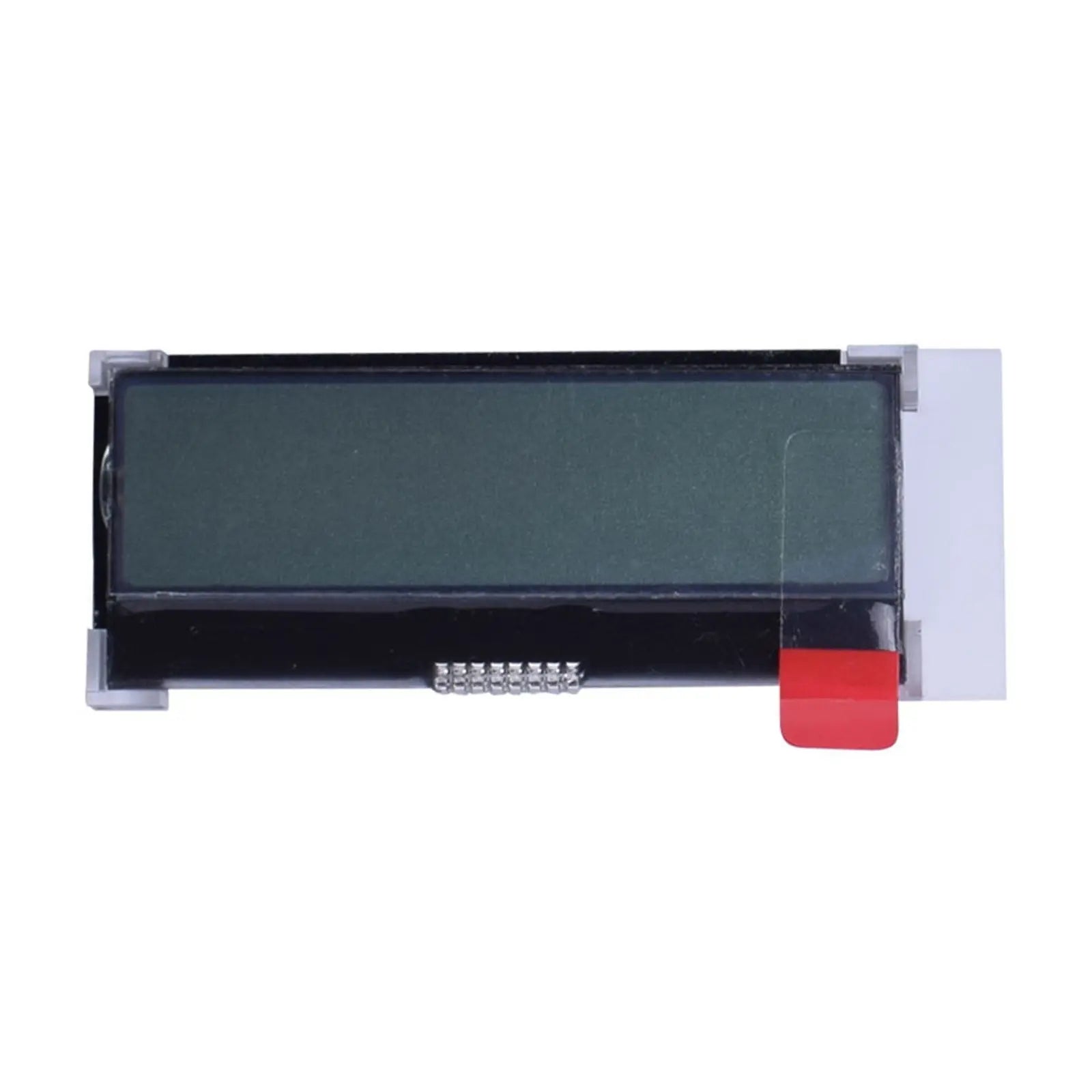
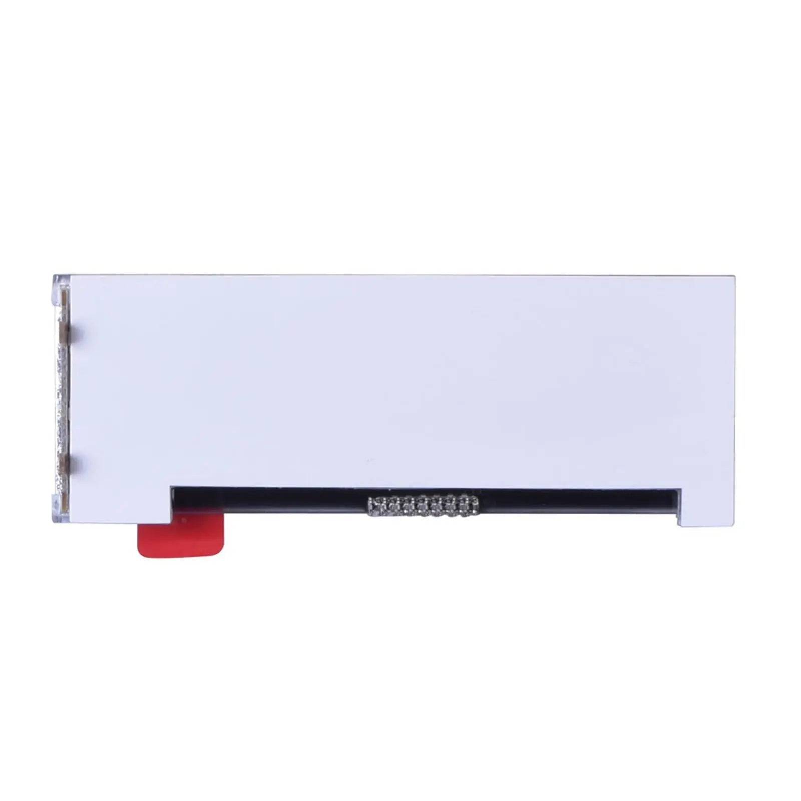

16x2 Character COG LCD Transflective Large - I2C
- 💹 Enjoy a 20% discount for orders over 500
- 📉 A 15% discount is available for orders ranging from 200 to 499
- 🎁 A 10% discount is available for orders ranging from 50 to 199
- 🎁 A 5% discount is available when ordering 10-49
Interested in customizing this product? Get in touch with us.
Order samples, immediate delivery.
Factory bulk lead time: 3 weeks.
16x2 Character COG LCD Transflective Large - I2C
- 💹 Enjoy a 20% discount for orders over 500
- 📉 A 15% discount is available for orders ranging from 200 to 499
- 🎁 A 10% discount is available for orders ranging from 50 to 199
- 🎁 A 5% discount is available when ordering 10-49
Resources & Downloads
16×2 Character COG LCD – FSTN Positive Transflective, I2C
DM-COG1602-712 is a 16-character by 2-line COG (Chip-on-Glass) LCD module with an FSTN positive transflective display, ST7032I controller IC, and I2C MPU interface. The module logic supply is specified at 3.0–5.0V, with 3.3V typical, and the specified weight is 11.3g.
The display is specified as transflective with a white LED backlight. Evaluate display readability, viewing direction, backlight operation, and mechanical fit in the final application.

Technical Specifications
The following specifications are based on the DM-COG1602-712 product datasheet. For complete electrical characteristics, optical performance, interface timing, and recommended application circuits, please refer to the official datasheet.
| Parameter | Specification |
|---|---|
| Product Model | DM-COG1602-712 |
| Display Format | 16 characters × 2 lines |
| LCD Type | FSTN Positive |
| Display Mode | Transflective |
| Controller IC | ST7032I |
| Interface | I2C MPU Interface |
| Power Supply (VDD) | 3.3V typical (3.0–5.0V range) |
| Duty / Bias | 1/16 duty, 1/5 bias |
| View Direction | 6:00 |
| Backlight | White LED |
| Operating Temperature | −20°C to +70°C |
| Storage Temperature | −30°C to +80°C |
| Weight | 11.3g |
Optical & Electrical Characteristics
The following electrical and optical values are specified in the DM-COG1602-712 module datasheet.
Pin Configuration & I2C Interface
The DM-COG1602-712 uses an 8-pin I2C MPU interface. SDA and SCL require pull-up resistors to the I2C bus supply. Follow the module reference circuit and mechanical drawing for PCB design.
I2C Bus Details
ST7032I Controller IC Features
The DM-COG1602-712 uses the ST7032I, the I2C version of the ST7032 dot-matrix LCD controller/driver family. The controller documentation specifies integrated display RAM, character-generator ROM/RAM, LCD driver circuitry, an internal oscillator, and a voltage booster/follower. The module I2C interface remains write-only.
I2C Timing Parameters
The following I2C timing parameters are based on the module datasheet and ST7032I controller documentation. The ST7032I controller documentation specifies tHIGH = 0.6µs minimum; refer to the full datasheets for complete timing diagrams and all parameters.
SCL Clock Frequency
SCL Low Period (tLOW)
SCL High Period (tHIGH)
Bus Free Time (tBUF)
START Setup Time (tSU:STA)
Bus Capacitance (Cb)
Example Application Considerations
The module specifications can be evaluated for embedded equipment that requires a 16 × 2 character display with an I2C MPU interface. Verify optical performance, electrical design, environmental conditions, and mechanical fit in the complete system.
Industrial Equipment
For equipment readouts and status displays operating within the specified −20°C to +70°C temperature range. Verify readability, viewing direction, backlight operation, and environmental conditions in the final installation.
Portable Instruments
For compact instruments requiring an I2C character display. The module logic current is specified at 0.18mA typical; total display power must also include the white LED backlight current.
Test & Measurement
For equipment requiring a compact alphanumeric display. Evaluate the specified 6:00 viewing direction against the final mounting orientation.
Consumer Electronics
For embedded equipment using an I2C interface. Confirm that MCU I/O levels meet the specified VIL/VIH requirements at the selected VDD voltage.
Reliability Test Conditions
The module datasheet lists the following reliability test conditions for engineering reference. They are not a statement that each shipped module is individually subjected to every listed test.
High Temp Storage
Endurance test at high storage temperature for extended duration.
80°C, 200hrsLow Temp Storage
Endurance test at low storage temperature for extended duration.
−30°C, 200hrsHigh Temp Operation
Electrical and thermal stress endurance test under operating conditions.
70°C, 200hrsLow Temp Operation
Electrical stress endurance under low temperature operating conditions.
−20°C, 200hrsHumidity Operation
High temperature and humidity test under no-load condition, excluding polarizer.
60°C, 90%RH, 96hrsThermal Shock
Thermal-shock resistance test using the reference profile shown in the datasheet: 30 minutes at −20°C, 5 minutes at 25°C, and 30 minutes at 70°C per cycle.
−20°C / 70°C, 10 cyclesVibration Test
Vibration endurance test during transportation and use. The specified condition is 1.5mm total fixed amplitude, 10–55Hz, a 60-second cycle, and 16 minutes in each of the X, Y, and Z directions; packaging is included in the test.
1.5mm, 10–55Hz, X/Y/Z, 16min/axisESD Test
Electrostatic discharge endurance test applied to module terminals.
800V, 1.5kΩ, 100pF, 1 timeEngineering Notes
Review the following module-datasheet and controller-documentation items before PCB layout and system validation.
Power-On and Reset
Review the ST7032I initialization sequence after VDD stabilizes. The module reference circuit shows RST pulled up to VDD through 10kΩ. If the internal reset conditions cannot be guaranteed, use the external reset function from the MCU as described in the controller documentation. The module datasheet includes example initialization code for 3V and 5V operation.
Booster Capacitor Configuration
Follow the module reference circuit for the selected supply voltage. At VDD = 3.0V, connect VOUT to VDD through a 1µF capacitor and connect CAP1N to CAP1P through a 1µF capacitor. At VDD = 5.0V, connect VOUT directly to VDD; CAP1N and CAP1P are marked NC. Do not use the 3.0V capacitor configuration for 5.0V operation.
I2C Pull-up Resistors
SDA and SCL require pull-up resistors to the I2C bus power. The module reference circuit shows 10kΩ pull-up resistors. Final resistor selection should be verified for bus capacitance (maximum 400pF), wiring length, supply voltage, and required I2C clock rate.
Voltage Level Matching
VDD supports 3.0V–5.0V operation. VIL is max 0.2×VDD and VIH is min 0.7×VDD, which are proportional thresholds. Confirm MCU I/O levels meet these requirements at your operating voltage.
I2C Slave Address
The ST7032I uses a fixed 7-bit slave address of 0111110. No address modification is possible. Confirm your MCU I2C library uses 7-bit or 8-bit address formatting correctly.
Backlight Drive
The white LED backlight is specified at VLED = 3.0–3.5V, with 3.3V typical, and ILED = 32mA typical / 40mA maximum at VLED = 3.3V. The product datasheet does not specify an external backlight resistor value; validate the drive method and current limit in the final system design.
I2C Write-Only Limitation
The ST7032I I2C interface supports writing data and instructions only. It cannot read data back from the controller, other than the I2C acknowledge signal. Use timing-based delays after commands instead of polling the busy flag through I2C.
Reference Documents
Use the official module datasheet and ST7032 controller documentation for dimensions, pin functions, electrical and optical limits, timing, initialization, and reliability test conditions.
Frequently Asked Questions
Common technical questions for integrating DM-COG1602-712 into a product design.
Q What I2C slave address does the module use?
The ST7032I controller uses a fixed 7-bit I2C slave address of 0111110. This address cannot be changed. Confirm your MCU I2C library uses the correct address format (7-bit vs 8-bit with R/W bit).
Q Can I read data back from the display via I2C?
No. The ST7032I I2C interface supports writing data and instructions only. It cannot read data back from the controller, except for the I2C acknowledge signal. Use timing-based delays instead of polling the busy flag.
Q How should the module be connected for 3V and 5V operation?
DM-COG1602-712 supports a 3.0–5.0V logic supply. At VDD = 3.0V, the reference circuit uses a 1µF capacitor between VOUT and VDD and a 1µF capacitor between CAP1N and CAP1P. At VDD = 5.0V, VOUT is connected directly to VDD, while CAP1N and CAP1P are marked NC.
Q Is the module compatible with 5V microcontrollers?
Yes, when the module is operated with VDD = 5.0V and the MCU I/O levels meet the specified thresholds: VIL ≤ 0.2×VDD and VIH ≥ 0.7×VDD. SDA and SCL require pull-up resistors to the I2C bus supply; verify the complete I2C voltage domain in the final circuit.
Q Can I use custom characters on this display?
Yes. The ST7032I provides 64 bytes of CGRAM supporting up to 8 user-defined 5 × 8 dot custom characters. The CGROM also includes 256 built-in character fonts.
Q What pull-up resistor values should I use for I2C?
The module reference circuit shows 10kΩ pull-up resistors on SDA and SCL. In a specific system, select and verify the final pull-up value according to bus capacitance (maximum 400pF), wiring length, supply voltage, and required I2C clock rate.
Download Official Datasheets
Download the module datasheet and controller documentation for dimensions, pin descriptions, electrical characteristics, optical data, I2C timing, command tables, font tables, initialization code, and reliability conditions.