

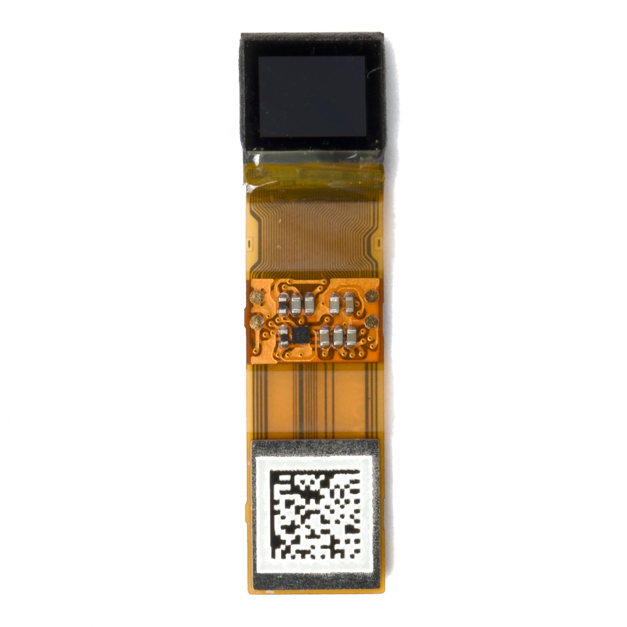
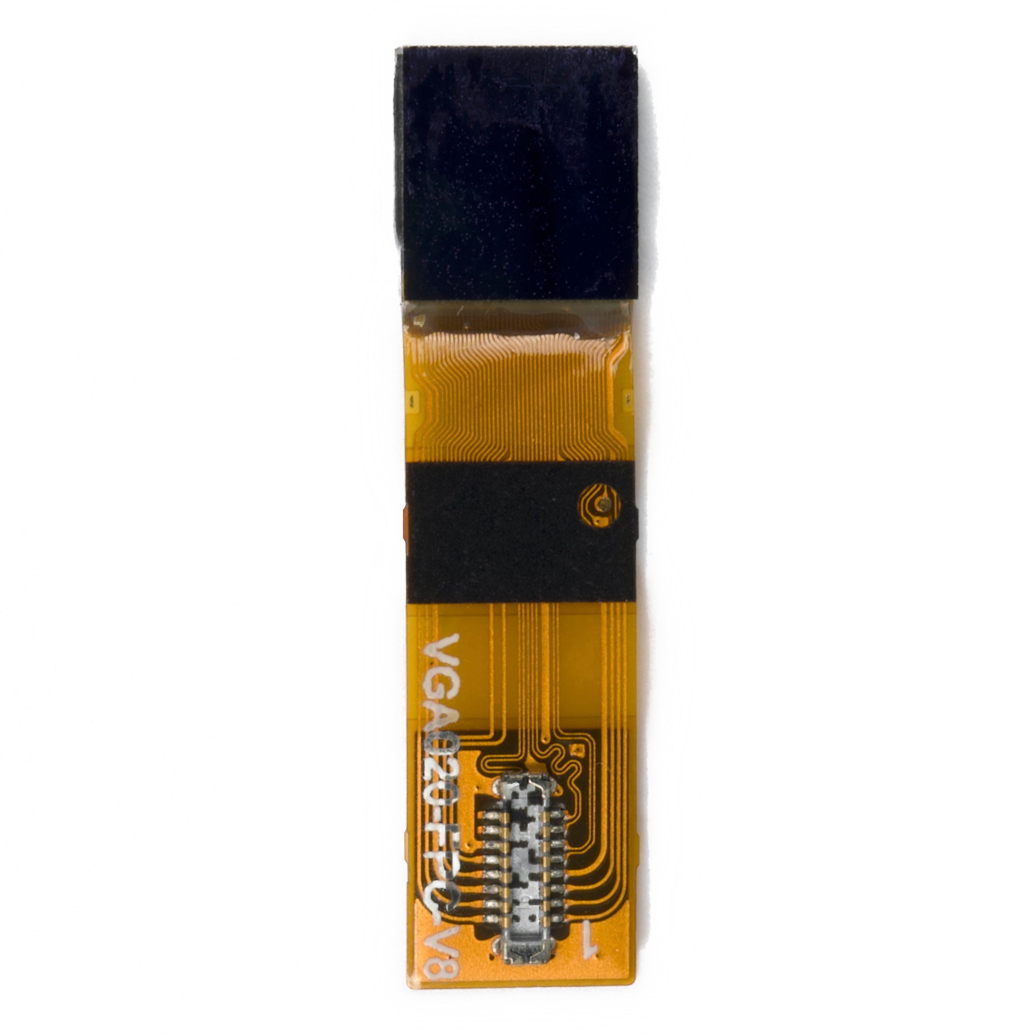
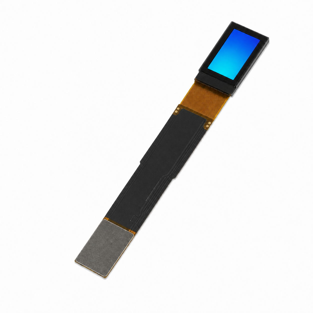
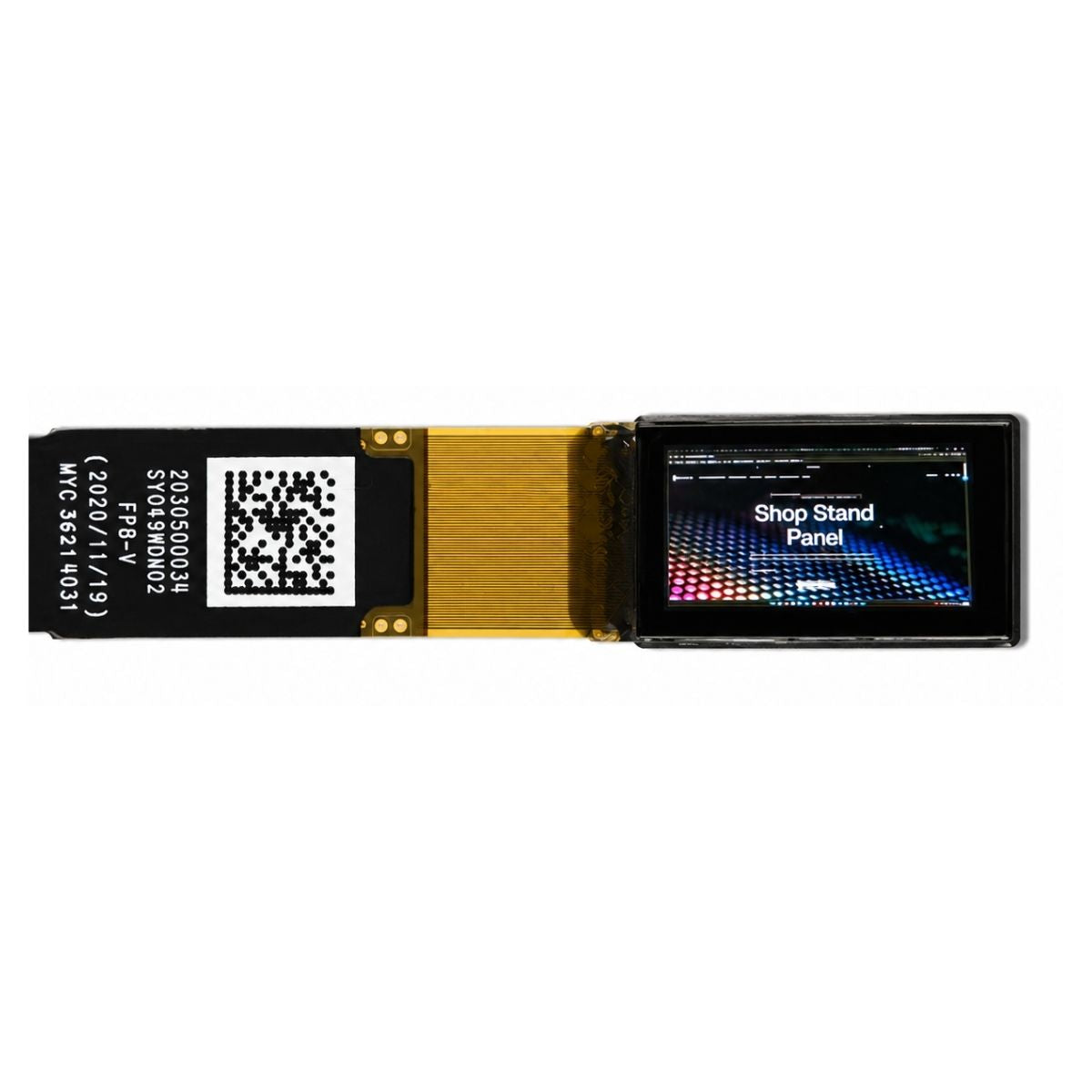


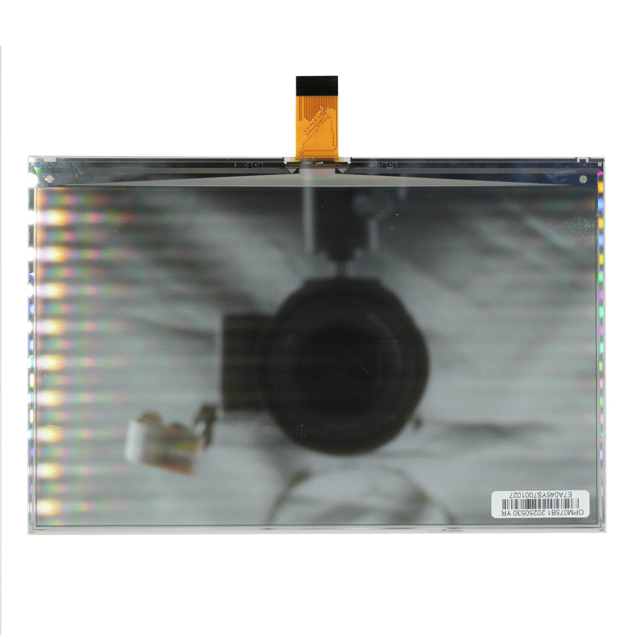
7.5" ePaper Display 800x480 - SPI
- 💹 Enjoy a 20% discount for orders over 500
- 📉 A 15% discount is available for orders ranging from 200 to 499
- 🎁 A 10% discount is available for orders ranging from 50 to 199
- 🎁 A 5% discount is available when ordering 10-49
Interested in customizing this product? Get in touch with us.
Order samples, immediate delivery.
Factory bulk lead time: 3 weeks.
7.5" ePaper Display 800x480 - SPI
- 💹 Enjoy a 20% discount for orders over 500
- 📉 A 15% discount is available for orders ranging from 200 to 499
- 🎁 A 10% discount is available for orders ranging from 50 to 199
- 🎁 A 5% discount is available when ordering 10-49
Resources & Downloads
DMAYE0750WVNA 7.5-Inch 800×480 ePaper Display
Pure Reflective AM EPD with Selectable 4-Wire or 3-Wire SPI
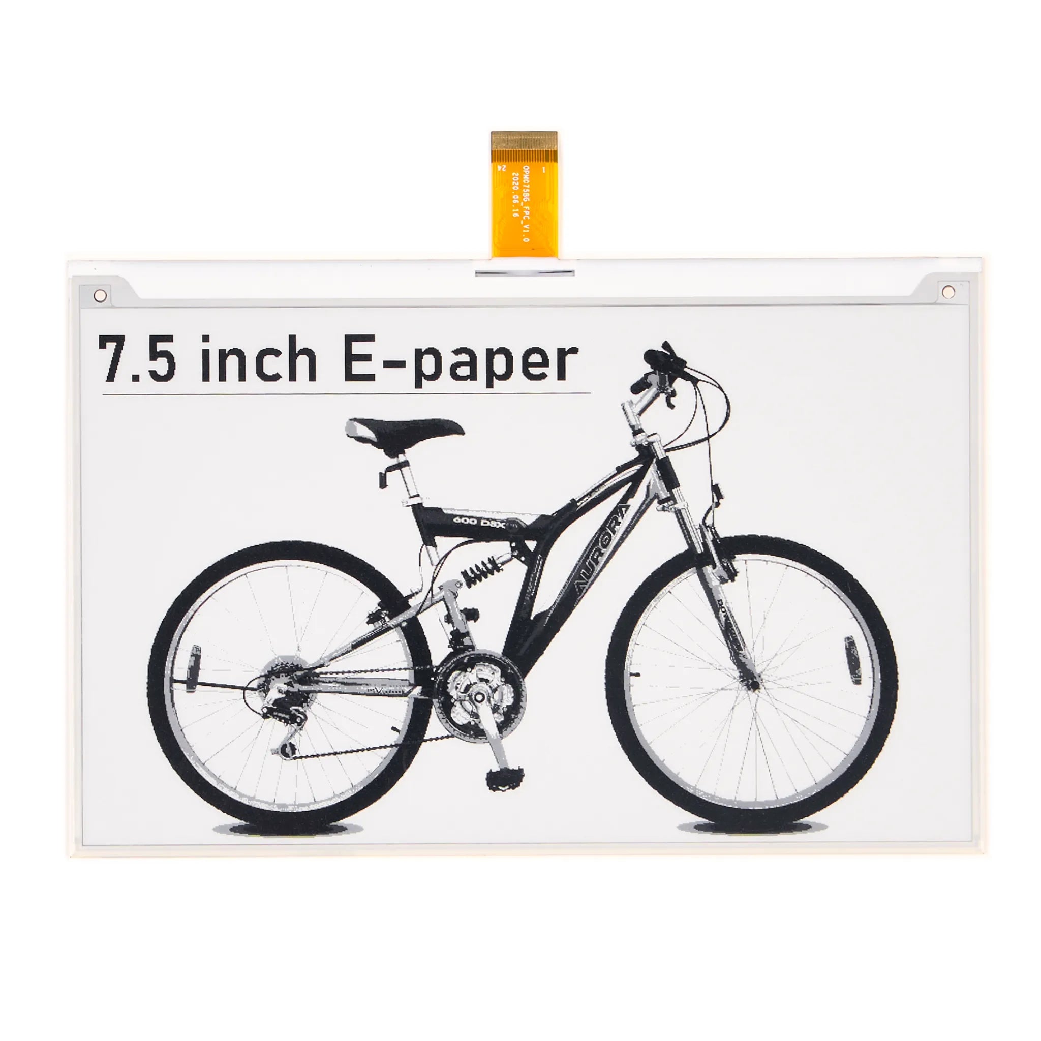
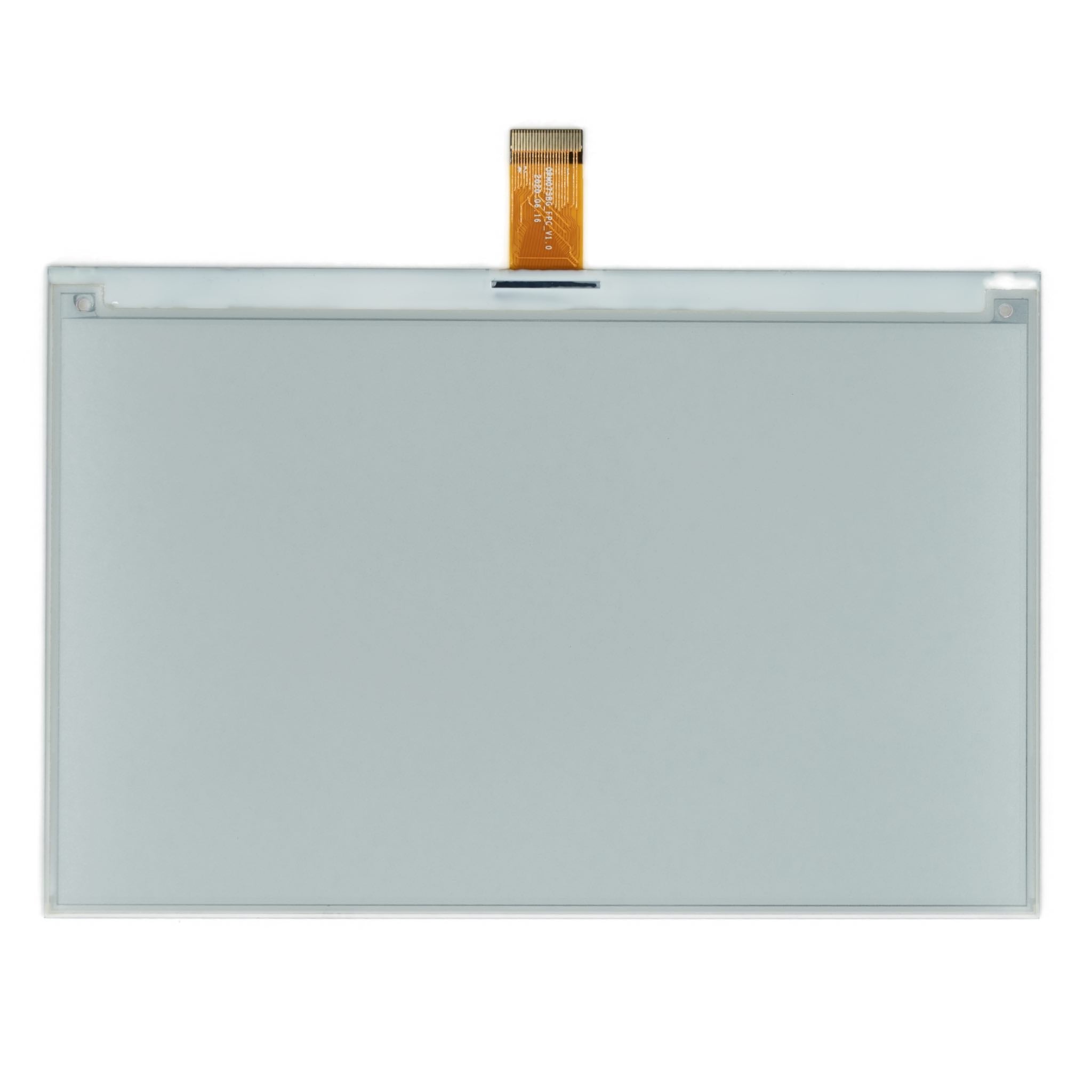
DMAYE0750WVNA is a 7.5-inch active-matrix electrophoretic display with 800(H)×480(V) pixels, a 163.2(H)×97.92(V) mm active area, and a 170.2(H)×111.2(V)×1.02(D) mm outline. The specification identifies the panel as pure reflective and bi-stable.
The module supports hardware-selectable 4-wire SPI and 3-wire 9-bit SPI. Integrated functions listed in the specification include gate and source buffers, an MCU interface, timing-control logic, an oscillator, a DC-DC converter, SRAM, LUT, and VCOM circuitry. The documented application is an electronic shelf label system.
Key Specifications
Documented values for product selection and integration.
Document reference: DMAYE0750WVNA Product Specification, V1.0.0, dated July 1, 2025. Use the linked specification and its mechanical drawing for component selection and PCB release.
Product Specifications
The values below are taken from the DMAYE0750WVNA Product Specification V1.0.0. Minimum, typical, and maximum values are shown only where the document defines them.
| Parameter | Specification |
|---|---|
| SKU | DMAYE0750WVNA |
| Display Technology | Active Matrix Electrophoretic Display (AM EPD) |
| Screen Size | 7.5 inch |
| Resolution | 800(H)×480(V) pixels |
| Active Area | 163.2(H)×97.92(V) mm |
| Pixel Pitch | 204(H)×204(V) µm |
| Pixel Configuration | Rectangle |
| Module Outline | 170.2±0.2(H)×111.2±0.2(V)×1.02±0.1(D) mm |
| Weight | 41 g |
| Display Mode | Pure reflective, bistable electrophoretic display |
| MCU Interface | 4-wire SPI or 3-wire 9-bit SPI, selected by the BS pin |
| Serial Access | Write-only in both SPI modes |
| Pin Count | 24 pins |
| Logic Supply Voltage | 2.8 V minimum, 3.0 V typical, 3.6 V maximum |
| Operating Temperature | 0°C to 50°C |
| Operating Illuminance | Indoor only; 2000 lux maximum |
| Storage Temperature | -25°C to 60°C |
| Storage Relative Humidity | 30%RH to 60%RH |
| White Reflectivity | 45% minimum, 48% typical |
| Contrast Ratio | 20:1 minimum, 25:1 typical |
| Full Refresh Time | 500 ms minimum, 750 ms typical at 25°C with the specified waveform |
| Partial Refresh Time | 250 ms typical at 25°C with the specified waveform |
| Panel Operating Power | 45 mW typical, 450 mW maximum under the datasheet transition test condition |
| Panel Operating Current | 15 mA typical, 150 mA maximum at VDD = 3.0 V |
| Sleep Current | 35 µA typical at VDD = 3.0 V with DC-DC off, no clock, and no output load |
| Deep-Sleep Current | 1 µA typical at VDD = 3.0 V with DC-DC off, no clock, no output load, and RAM data not retained |
| Deep-Sleep Power | 3 µW typical |
| Temperature-Sensor Interface | TSCL and TSDA provide an I2C master interface for an external digital temperature sensor |
| RoHS | Marked as compliant in the supplied specification |
Document limits: The specification does not identify a controller part number, mating connector part number, or touch-panel configuration. CE and FCC are marked as not certified. The 45 mW typical panel-power value is measured during the documented two-gray-scale transition test; electrical and optical characteristics are guaranteed only with the controller and waveform specified by the panel provider.
Display and Refresh Characteristics
The display operates in pure reflective mode. Optical and refresh performance must be evaluated under the measurement conditions and waveform requirements stated in the datasheet.
Reflective Optical Performance
White reflectivity is specified at 45% minimum and 48% typical. Contrast ratio is specified at 20:1 minimum and 25:1 typical. The feature list states an ultra-wide viewing angle, but no numeric viewing-angle range is provided.
Bi-Stable Operation
The specification identifies the panel as bi-stable and separately lists operating, sleep, and deep-sleep power or current values.
Full Refresh
Full refresh is specified at 500 ms minimum and 750 ms typical at 25°C. The screen flickers several times during the refresh process, and the specified waveform is required.
Partial Refresh
Partial refresh is specified at 250 ms typical at 25°C. The specification states that the screen does not flicker during the partial-refresh process, and the specified waveform is required.
Optical test method: Measurements are made with illumination at 45 degrees and detection perpendicular to the panel unless otherwise stated. White reflectivity is measured with an Eye-One Pro spectrophotometer, and contrast ratio is calculated from all-white and all-black surface reflectance.
SPI Interface Options and Control Signals
The module supports two hardware-selected serial interfaces. Both modes are write-only. CSB must be low for MCU communication, and the host must not send commands while BUSYN is high.
Interface Selection
BS = Low: 4-wire SPI using SDIN, SCLK, CSB, D/C, and RSTN.
BS = High: 3-wire 9-bit SPI using SDIN, SCLK, CSB, and RSTN. Each transfer contains the D/C bit followed by D7 through D0.
Serial data is shifted into the controller on the rising edge of SCLK.
24-Pin Assignment
Use the pin numbering and FPC orientation shown in the official mechanical drawing. NC pins must not be connected to each other.
| Pin | Name | Function |
|---|---|---|
| 1 | NC | No connection. Do not connect to other NC pins. |
| 2 | GDR | N-channel MOSFET gate-drive control output. |
| 3 | RESE | Current-sense input for the control loop. |
| 4 | NC | No connection. Do not connect to other NC pins. |
| 5 | VDHR | Positive source-driving voltage 1 capacitor pin. |
| 6 | TSCL | I2C clock output for an external digital temperature sensor. |
| 7 | TSDA | I2C bidirectional data for an external digital temperature sensor. |
| 8 | BS | Bus-interface selection input: low for 4-wire SPI; high for 3-wire 9-bit SPI. |
| 9 | BUSYN | Busy-state output. |
| 10 | RSTN | Active-low reset input. |
| 11 | D/C | Data/command control input for 4-wire SPI. |
| 12 | CSB | Active-low chip-select input. |
| 13 | SCL | SPI serial-clock input. |
| 14 | SDA | SPI serial-data input. |
| 15 | VDD | Power supply for interface logic pins. |
| 16 | VDD | Power supply for the controller chip. |
| 17 | VSS | Ground. |
| 18 | VDDD | Core-logic power pin. A capacitor must be connected between VDDD and VSS under all circumstances. |
| 19 | VPP | Power supply for OTP programming. |
| 20 | VSH | Positive source-driving voltage 2 capacitor pin. |
| 21 | VGH | Positive gate-driving voltage capacitor pin. |
| 22 | VSL | Negative source-driving voltage capacitor pin. |
| 23 | VGL | Negative gate-driving voltage capacitor pin. |
| 24 | VCOM | VCOM driving-voltage capacitor pin. |
Electrical Limits and Serial Timing
Recommended operating values must be used for normal operation. Absolute maximum ratings identify limits beyond which device damage may occur and are not normal operating conditions.
| Electrical Item | Documented Value |
|---|---|
| Absolute Maximum Logic Supply | -0.5 V to +4.0 V |
| Absolute Maximum Logic Input | -0.5 V to VDD + 0.5 V |
| Absolute Maximum Logic Output | -0.5 V to VDD + 0.5 V |
| Recommended VDD | 2.8 V minimum, 3.0 V typical, 3.6 V maximum |
| High-Level Input Voltage | 0.8×VDD minimum |
| Low-Level Input Voltage | 0.2×VDD maximum |
| High-Level Output Voltage | 0.9×VDD minimum at IOH = -100 µA |
| Low-Level Output Voltage | 0.1×VDD maximum at IOL = 100 µA |
| OTP Programming Voltage | 7.5 V typical at VPP; this is not the normal VDD supply |
| Serial Timing Parameter | Specification |
|---|---|
| Timing Conditions | VDD - VSS = 2.4 V to 3.3 V, TOPR = 25°C, CL = 20 pF |
| Clock Cycle Time, tcycle | 250 ns minimum |
| Address Setup Time, tAS | 150 ns minimum |
| Address Hold Time, tAH | 150 ns minimum |
| Chip-Select Setup Time, tCSS | 120 ns minimum |
| Chip-Select Hold Time, tCSH | 60 ns minimum |
| Write-Data Setup Time, tDSW | 50 ns minimum |
| Write-Data Hold Time, tDHW | 15 ns minimum |
| Clock Low Time, tCLKL | 100 ns minimum |
| Clock High Time, tCLKH | 100 ns minimum |
| Rise Time, 20%-80% | 15 ns maximum |
| Fall Time, 20%-80% | 15 ns maximum |
Operating, Storage, and Handling Requirements
The EPD module contains fragile glass and plastic materials. Handle the panel carefully and follow the documented operating, storage, cleaning, and environmental requirements.
Specified Environment
Operate the panel from 0°C to 50°C. Store it from -25°C to 60°C at 30%RH to 60%RH. The operating illuminance entry is listed as indoor only, with 2000 lux as the maximum.
Mechanical Handling
Protect the panel from drops. Do not bend, twist, press, disassemble, reassemble, or stack panels. Do not connect or disconnect the interface while the panel is operating.
Surface Cleaning
Use a soft, dry cloth without chemicals. The protection film is soft and has no hard coating; pressure or abrasive cleaning may cause dents or scratches.
Moisture and Light Exposure
Prevent moisture penetration, frost, and condensation. Do not expose an unprotected panel to high temperature, high humidity, sunlight, or fluorescent light for extended periods.
Recommended Warehouse Storage
Keep the panel in its original packaging without sunlight or condensation at 15°C to 35°C and 30%RH to 60%RH.
Chemical Environment
Do not expose the module to harmful acid or alkali gases that may corrode electronic components.
Reliability Test Conditions
The following values are qualification stress conditions stated in the datasheet. They are not continuous-use ratings and do not replace the specified operating and storage ranges.
| Test | Documented Condition | Method / Remark |
|---|---|---|
| High-Temperature Operation | +50°C, 30%RH for 168 hours | IEC 60068-2-2Bp |
| Low-Temperature Operation | 0°C for 168 hours | IEC 60068-2-2Ab |
| High-Temperature Storage | +70°C, 23%RH for 168 hours | IEC 60068-2-2Bp |
| Low-Temperature Storage | -25°C for 168 hours | IEC 60068-2-1Ab |
| High-Temperature, High-Humidity Operation | +40°C, 90%RH for 168 hours | IEC 60068-2-3CA |
| High-Temperature, High-Humidity Storage | +60°C, 80%RH for 168 hours | IEC 60068-2-3CA |
| Thermal Shock | 100 cycles; -25°C for 30 minutes followed by +70°C for 30 minutes per cycle | IEC 60068-2-14 |
| Package Vibration | 1.04G, 10-500 Hz, X/Y/Z directions, one hour in each direction | Fully packed for shipment |
| Package Drop Impact | 122 cm onto concrete; one corner, three edges, and six faces, one drop each | Fully packed for shipment |
| Non-Operating Electrostatic Effect | Machine-model test at ±250 V | IEC 62179 and IEC 62180 |
| Post-Test Requirement | Electrical, mechanical, and optical specifications must remain satisfied after the stated tests | Applies to the reliability tests above |
Selection and Integration Checks
Before ordering or releasing a PCB, review the mechanical drawing, pin assignment, electrical limits, SPI timing, waveform requirement, block diagram, and typical application circuit. The specification does not identify a mating connector part number, controller part number, or touch-panel configuration.
Mechanical fit: Verify the 170.2±0.2×111.2±0.2×1.02±0.1 mm outline, active area, FPC orientation, and enclosure clearances.
Power circuit: Follow the typical application circuit for GDR, RESE, VDHR, VSH, VGH, VSL, VGL, VCOM, VDDD, and the required external components.
Firmware: Validate reset, SPI timing, BUSYN monitoring, the specified waveform, full and partial refresh, and sleep-mode entry.
Optical evaluation: Evaluate reflectivity and contrast under the intended lighting, and protect the panel from moisture, condensation, prolonged sunlight, and prolonged fluorescent-light exposure.
Common Questions
Is the panel specified as bi-stable?
The specification identifies the panel as bi-stable and lists separate operating, sleep, and deep-sleep power or current values.
Is this panel specified for outdoor use?
No outdoor rating is stated. The operating table lists indoor-only use with 2000 lux as the maximum, and the handling section warns against prolonged sunlight exposure of an unprotected panel.
Which SPI mode is supported?
BS low selects 4-wire SPI. BS high selects 3-wire 9-bit SPI. Both modes are write-only.
What conditions apply to the 250 ms partial-refresh value?
The documented value is 250 ms typical at 25°C and requires the specified waveform.
Is a touch panel included?
No touch-panel specification is provided in the supplied datasheet. Confirm separately before ordering if touch functionality is required.
What controller IC is used?
The supplied V1.0.0 specification describes integrated controller functions but does not identify a controller part number. Confirm with DisplayModule when the exact controller identification is required.
Download Official Datasheet
Review the official DMAYE0750WVNA specification for the mechanical drawing, 24-pin assignment, electrical limits, SPI timing, optical measurement method, reliability conditions, block diagram, and typical application circuit.