


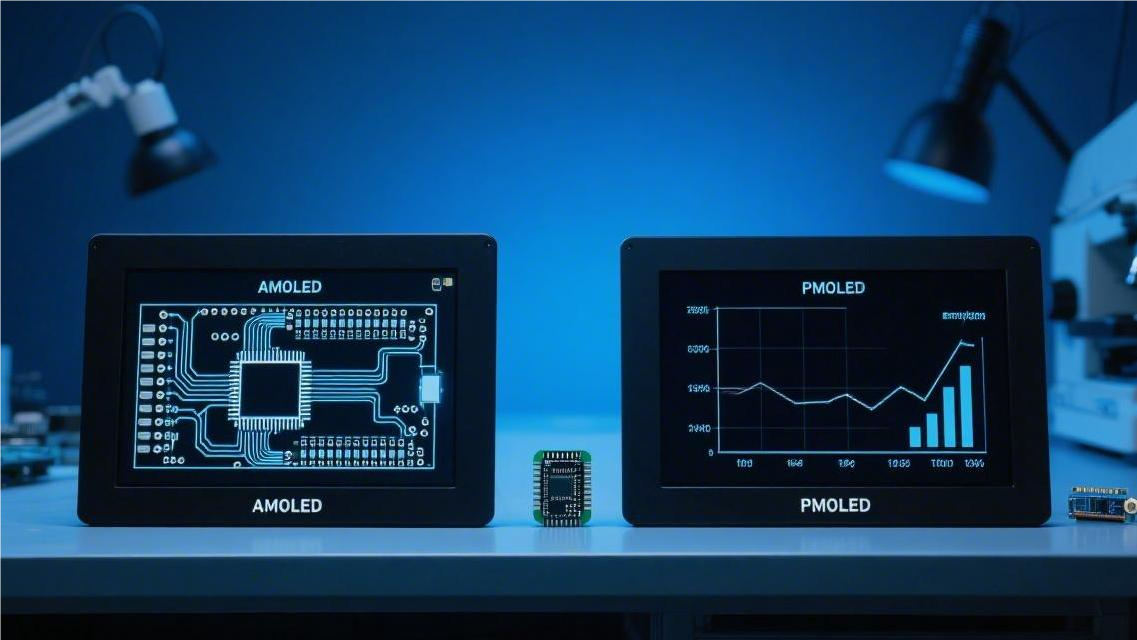
AMOLED vs PMOLED | Driving Method, Size Limits & Cost
AMOLED utilizes a TFT array for active driving, where pixels are independently controlled, allowing sizes to exceed 100 inches. Although the cost is high, the picture quality is exquisite;
PMOLED relies on row-and-column scanning for passive driving, and due to voltage drop limitations, its size is usually less than 3 inches. Because of its extremely simple structure, the cost is only about 30% of the former, and it is mostly used in small wearable devices.
Driving Method
PMOLED relies on high-voltage current pulses at the intersections of row and column electrodes to emit light. Limited by a low duty cycle of 1/64 to 1/256, the instantaneous brightness of a single pixel must reach dozens of times the average value, and the driving voltage is usually maintained at 15V-20V.
AMOLED utilizes a TFT backplane and storage capacitors to lock the voltage, enabling pixels to emit light continuously at a constant current under 3V-5V, eliminating flicker and significantly reducing power consumption.
Passive Matrix (PMOLED)
Under a 1/128 duty cycle, each row of pixels only receives about 130 microseconds of lighting time within a 16.7-millisecond frame period, remaining turned off for the rest of the time.
Since there are no capacitors to store charge, the driving IC must pump high-intensity current into the electrodes in a very short time, forcing the pixels to generate an instantaneous brightness exceeding 10,000 nits so that the average brightness perceived by the human eye is maintained at 100-150 nits. This high-voltage driving environment typically requires an external bias voltage of 15V to 20V, much higher than the 3.3V of standard CMOS logic circuits, increasing the complexity of DC-DC conversion circuits.
Physical Layer Composition:
- Anode Array: Uses an Indium Tin Oxide (ITO) glass substrate with a thickness of approximately 100nm to 150nm.
- Organic Functional Layer: Contains the Hole Transport Layer (HTL) and Emission Layer (EML), with a total thickness of less than 200nm.
- Cathode Separators: Inverted trapezoidal structures formed by photolithography, approximately 3μm to 5μm high, ensuring physical isolation of the cathode strips.
- Metal Cathode: Vapor-deposited Al (Aluminum) or Ag (Silver), with resistivity controlled to within a few ohms per square centimeter.
This structure eliminates the expensive TFT (Thin-Film Transistor) masking process, reducing the number of masks from the 10-14 layers required by AMOLED to 4-6 layers. Because the production equipment requires a vacuum level of 10⁻⁶ Pa and does not involve high-temperature annealing processes, the substrate utilization rate for a single 2-inch panel is as high as 90%. However, as the number of rows increases, the current energy allocated to a single row is diluted, resulting in a linear decrease in overall screen brightness.
Electrical Performance Data:
- Response Time: Maintained at the microsecond (μs) level, about 1000 times faster than regular LCDs.
- Contrast Ratio: Can reach 10,000:1 in dark laboratory environments.
- Power Consumption Curve: About 20mW during text display (10% pixels lit), soaring to over 150mW on an all-white screen.
- Resolution Bottleneck: The pixel pitch is typically above 0.2mm, making it difficult for PPI to exceed 150.
In actual operation, the row resistance of PMOLED becomes the primary heat source, and ITO traces that are several centimeters long will generate a significant voltage drop. When current passes through a 128x64 array, the brightness difference between the terminal and initial pixels can reach about 10%. This usually requires a dedicated Reverse Bias technology built into the driver chip to suppress crosstalk currents between pixels.
To prevent the light-emitting layer from overheating under high current, which shortens the T50 lifespan (the time it takes for brightness to drop to half its initial value), engineers often limit the operating current to between 10μA and 40μA. Because PMOLED does not require cooling and its components are thin and light (total thickness often less than 1.5mm), it can still maintain a normal refresh rate in a freezing environment of minus 40°C, without the severe ghosting/smearing typical of LCD screens.
Typical Application Specifications:
- 0.91 Inches: 128x32 resolution, commonly found in entry-level fitness trackers.
- 1.3 Inches: 128x64 resolution, standard for industrial instrument interfaces.
- 2.4 Inches: 320x240 resolution, which is close to the physical limits of passive driving.
- Interface Protocols: Broadly supports I2C, 4-wire SPI, and 8-bit parallel ports.
As the production scale expands, the depreciation costs of PMOLED panel production lines have dropped to extremely low levels. In the Bill of Materials (BOM) for a single module, the Driver IC and Flexible Printed Circuit (FPC) account for about 60% of the cost. Despite the power consumption bottleneck, this low-cost solution remains the preferred choice for embedded devices that do not require complex animations and only need to display white, green, or blue characters.
Active Matrix (AMOLED)
Taking a 6.7-inch 1440p screen as an example, the panel integrates over 11 million independent pixel circuits to precisely control the amount of current passing through the organic light-emitting layer. The most basic circuit topology usually adopts a 2T1C (two transistors and one capacitor) structure.
When the Scan Line writes the data voltage, the Storage Capacitor charges to a range of 1V to 3V. After the scanning cycle ends, the row drive pulse disconnects, but the dozens of picofarads (pF) of charge stored internally can maintain the conduction state of the driving transistor's gate. The pixel maintains nearly 100% emission duration throughout a complete 16.7 millisecond (60Hz) frame period.
The organic layer does not need to withstand extremely high transient pulses; an extremely low current density of around 3A/cm² is sufficient to reach a peak brightness of 1000 nits. The internal power supply of the panel is divided into a positive pole (ELVDD, usually set around 4.6V) and a negative pole (ELVSS, typically varying between -1.5V to -4.0V). The extremely small steady-state constant current significantly delays the thermal quenching speed of excitons in organic materials.
-
LTPS (Low-Temperature Polycrystalline Silicon): Processed via excimer laser annealing, with an electron mobility exceeding 100 cm²/Vs, mostly used in high-density mobile phone screens above 500 PPI.
-
Oxide (IGZO): Indium Gallium Zinc Oxide has extremely low leakage current (10⁻¹² A level), supporting 12.9-inch tablets lowering their refresh rate to 10Hz to save power.
-
LTPO (Low-Temperature Polycrystalline Oxide): Combining both of the above, it supports dynamic refresh rates from 1Hz to 120Hz, potentially reducing overall panel power consumption by about 15% to 20%.
TFT arrays experience threshold voltage (Vth) drift during large-area manufacturing, so high-end panels have universally upgraded to 7T1C or even more complex pixel circuits. The added transistors are specifically responsible for measuring and compensating for internal voltage deviations, ensuring that the brightness uniformity of 33 million pixels on a 77-inch 8K panel reaches over 95%. Response time is compressed to under 0.1 milliseconds, eliminating physical ghosting in high-speed motion images.
| Specification Parameter | Data Range | Technical Reference |
|---|---|---|
| Number of Mask Layers | 10 to 15 layers | Depends on TFT topology complexity |
| Dynamic Contrast Ratio | 1,000,000:1 | Pure black state without background backlight |
| Total Emissive Layer Thickness | 100nm to 200nm | Includes hole transport and electron injection layers |
| T50 Test Lifespan | > 30,000 hours | Test baseline is 500 nits brightness |
Building a production line with a monthly capacity of 30,000 sheets (Gen 6 line, substrate size 1500mm x 1850mm) often requires an initial equipment investment exceeding 5 billion USD. Vacuum Evaporators and high-precision Fine Metal Masks (FMM) account for massive expenditures. The aperture precision of the FMM must be strictly controlled within 2 micrometers (μm) to prevent red, green, and blue light-emitting materials from color mixing during evaporation.
To avoid the problem of blue light materials degrading too quickly at high resolutions, manufacturers adopt sub-pixel rendering technologies like Diamond or PenTile arrangements. The areas of red and blue sub-pixels are enlarged to 1.5 to 2 times that of the green sub-pixels. In a panel nominally rated at 400 PPI, the true density of the green sub-pixels is 400 PPI, while the physical density of the red and blue lights is only 283 PPI.
The Display Driver IC (DDI) is responsible for converting digital image signals into analog voltages, usually graded as 10-bit (1024 grayscale levels) or 12-bit. When displaying pure black content, the DDI cuts off the corresponding pixel's TFT gate voltage, dropping the operating current to the nanoampere (nA) level. All-white screen power consumption might reach 5 watts (W), while the average power consumption when playing dark-colored videos is only 1.2 watts.
Every layer of semiconductor photolithography process may introduce particle contamination, and the overall yield rate in the early stages of mass production is often below 60%. If a storage capacitor shorts out, the corresponding pixel will uncontrollably remain permanently on or permanently off. Before leaving the factory, optical inspection equipment (AOI) locates defects, and a laser is used to cut the damaged pixel wiring, turning it into an unnoticeable dark dot.
Replacing the rigid glass substrate at the bottom with a polyimide (PI) film just 10 to 50 micrometers thick forms the physical foundation for flexible screens. The PI film can withstand the 450°C high temperatures required for TFT curing, and upon completion, it is detached from the glass carrier board using a Laser Lift-off process. Finished panels can achieve a bending radius of less than 1.5 millimeters and withstand over 200,000 folding tests.
Size
PMOLED is limited by the 1/N duty cycle; an increase in rows leads to a surge in instantaneous current that burns out the organic material. As a result, its display panels are usually locked under 3 inches, and resolutions rarely exceed 256x128.
AMOLED relies on TFT capacitors to achieve 100% duty cycle light emission, requiring a driving voltage of only 3V-5V. This supports a span ranging from a 1.4-inch watch dial to a 97-inch TV, with PPI easily exceeding 500.
Size Comparison
When the screen reaches 3 inches (about 7.6 cm), since a single row only lights up for 1/240th of a second, the instantaneous current must surge to more than 200 times the average. This physical load locks the expansion path for PMOLED, concentrating its resolution mostly between 128x32 to 256x64.
In contrast, AMOLED equips each pixel with a capacitor through TFT (Thin-Film Transistors), achieving constant light emission at a 100% duty cycle. This driving method maintains the operating voltage in a low-voltage range of 3V to 5V, supporting sizes ranging from a 1.4-inch (3.5 cm) circular watch dial to a 97-inch (246 cm) ultra-large TV, with pixel density (PPI) easily crossing the 500 threshold.
| Physical Characteristics Indicator | PMOLED (Passive Matrix) | AMOLED (Active Matrix) |
|---|---|---|
| Maximum Commercial Size | Typically <= 3.0" | = 100" |
| Pixel Arrangement Precision | 0.15mm - 0.25mm pitch | 0.04mm - 0.08mm pitch |
| Typical Current Load | 100mA - 300mA transient pulse | 1μA - 10μA constant current |
| Substrate Driving Layers | 2 intersecting electrode layers | 5 - 9 layers mask process |
PMOLED's cathodes and anodes intersect in a crisscross pattern, and each Scan Line must carry the sum of the current for all pixel dots in that row. On a 2.4-inch panel, the current stress on a single pin often causes the heat generation in the ITO (Indium Tin Oxide) conductive layer to exceed 50°C, accelerating the physical degradation of the organic thin film.
Due to the lack of independent charge storage units, PMOLED cannot handle high-frequency image signals. When the display area expands to the size of a mobile phone, RC (Resistor-Capacitor) delay effects cause severe waveform distortion as signals travel to the edges of the screen. This leads to a brightness deviation (Uniformity) between the top and bottom of the screen often exceeding 20%, far below the standard of less than 5% required for commercial displays.
AMOLED's size advantage stems from LTPS (Low-Temperature Polycrystalline Silicon) or Oxide backplane technologies. In a 6.7-inch phone screen, each sub-pixel takes up only about 40 micrometers of space but integrates at least 2 transistors and 1 capacitor. This high degree of integration allows over 250,000 emissive units to be squeezed into 1 square inch without risking current overload.
In the field of large-sized TVs, IGZO (Indium Gallium Zinc Oxide) technology has become key to AMOLED's expansion. IGZO's electron mobility is 20 to 50 times that of traditional amorphous silicon, maintaining extremely low voltage drops on ultra-long signal lines for panels over 80 inches. This ensures that all 8.2 million pixels at 4K resolution (3840x2160) receive a uniform voltage distribution, guaranteeing consistent brightness across the entire large screen.
Physical flexibility is also part of the size equation. PMOLED uses rigid glass approximately 0.7mm to 1.1mm thick as a support because high-frequency, high-voltage driving requires a solid physical structure to prevent electrode fractures. AMOLED, however, can peel off the glass substrate in favor of a PI (Polyimide) film that is 10 to 20 micrometers thick, realizing special physical forms such as folding, stretching, or rolling.
In actual industrial design, because the module width of PMOLED needs to reserve a large amount of Fan-out routing space around the edges, its screen-to-body ratio is usually below 60%. In contrast, AMOLED utilizes the COP (Chip on Plastic) packaging process, allowing the driver chip to be bent directly onto the back of the screen. This achieves ultra-narrow bezel designs, bringing the effective display area to over 90% of the device's front footprint.
Passive Matrix Limitations
The structure of PMOLED consists of mutually perpendicular anode rows and cathode columns, where its pixels only light up at the instant the row and column are selected. In this 1/N duty cycle operation mode, if the screen has 128 rows, a single pixel is in the ON state for only 0.78% of a complete frame cycle.
To achieve a visibly average brightness to the naked eye within such a short time, the system must drastically increase the transient driving voltage. This voltage fluctuation is usually maintained between 15V to 20V, much higher than the 3.3V of logic circuits. This high-voltage pulse causes the power consumption of the Driver IC to grow geometrically as the number of rows increases.
-
Transient Brightness Overload: To achieve an average brightness of 100 cd/m², the instantaneous brightness under a 1/128 duty cycle must reach 12,800 cd/m².
-
Accelerated Material Decay: The luminous efficiency of organic materials drops drastically under ultra-high brightness, a phenomenon known as Singlet-Triplet Annihilation.
-
Thermal Accumulation Effect: Over 80% of the electrical energy input is converted into heat, causing the center temperature of the panel to rise by 10°C to 15°C after 10 minutes of continuous operation.
When the current density exceeds 50 mA/cm², the recombination area of holes and electrons within the emissive layer shifts, causing chromaticity coordinates to deviate from the origin. In long-term operation, this current stress triggers the physical and chemical degradation of the organic thin film, shortening its half-life to less than 5,000 hours.
Resistor-Capacitor Delay (RC Delay) limits increases in refresh rate. The ITO (Indium Tin Oxide) conductive layer used by PMOLED has a sheet resistance of about 10-15 Ω/sq. In panels larger than 3 inches, the delay for signals traveling from the driving end to the terminal pixels often exceeds 5 microseconds, which directly causes ghosting on the screen.
| Limitation Dimension | Typical Parameter Index | Description of Impact on Performance |
|---|---|---|
| Max Driving Rows | Usually ≤ 240 rows | Exceeding this limit causes transient currents to break down the organic functional layer. |
| Electrode Line Resistance | 10 Ω to 100 Ω | Generates significant IR drop, causing screen brightness non-uniformity to exceed 15%. |
| Driver Chip Pins | 300 to 500 Pins | High resolutions require numerous pins; a single IC accounts for over 40% of total module costs. |
| Refresh Rate Range | 45Hz to 75Hz | Cannot support high-speed dynamic image displays above 120Hz. |
Parasitic capacitance between electrodes can cause severe Cross-talk phenomena. When the pixels in a certain row are lit, pixels in adjacent rows emit faint light due to capacitive charging and discharging effects. This light leakage causes PMOLED's static contrast ratio, although high in lab settings, to frequently drop to 2000:1 when actually displaying complex images.
The physical compression of routing space limits resolution. At a precision of 200 PPI, the width of the insulating layer (PDL) between row and column electrodes must be compressed to under 10 micrometers. If pixel density is increased further, the electric field strength between electrodes risks triggering air breakdown or short circuits, causing production yield rates to plummet from 90% to under 50%.
-
Fan-out Routing Redundancy: The edges of the screen require 3mm to 5mm of reserved routing area, making it difficult for the effective display area (screen-to-body ratio) to break through 70%.
-
Non-linear Power Consumption Growth: When displaying a white background, the total machine current can instantly soar to 250mA, which is 3 to 5 times that of an equivalent-sized AMOLED.
-
Grayscale Control Precision: Relying on Pulse Width Modulation (PWM) to control grayscale results in noticeable Flicker at low brightness.
Because the turn-on voltage (Vth) of RGB sub-pixels varies, the passive matrix struggles to achieve precise color balance via simple voltage pulses. Under the 65K color specification, inconsistent decay rates of the three colors of light will cause obvious color shifts after the screen has been used for 1,000 hours.
PMOLED's ITO electrodes are highly prone to generating micro-cracks during repeated bending, and the resistance value can instantly increase by over 5 times. Lacking a TFT compensation circuit, this change in resistance is directly reflected in screen brightness, creating visual bright and dark patches.
In the loop of every frame, the proportion of time a pixel is in an off state exceeds 99%. This extremely low light-on time utilization renders PMOLED's readability extremely poor in bright outdoor environments; even with added backlight compensation, peak brightness is hard to stabilize above 500 nits.
Traditional SPI or I2C interfaces can only support low-resolution instruction transmission. To drive a 320x240 true-color image, data bandwidth requirements will exceed 100 Mbps. This necessitates equipping more expensive parallel interface driver chips, further driving up the total system cost of what is ostensibly positioned for the budget market.
Active Matrix Large Screens
Behind every pixel point in an AMOLED is an integrated driving circuit comprised of at least two Thin-Film Transistors (TFT) and one Storage Capacitor (Cs). This structure achieves a 100% duty cycle, allowing the pixels to emit light continuously throughout the frame without needing high-frequency pulses like a passive matrix.
This driving mode reduces a single pixel's current load from milliamperes to the nanoampere (nA) level, solving the hazard of large-area organic materials burning out under high-voltage pulses. Driving voltages are maintained in the low-voltage range of 3.3V to 4.6V, supporting sizes ranging from a 1.4-inch (about 3.5 cm) watch dial to a 97-inch (about 246 cm) ultra-large TV.
In a 6.7-inch smartphone panel, Low-Temperature Polycrystalline Silicon (LTPS) technology provides an electron mobility of up to 100 cm²/(V·s). This conductive efficiency permits complex compensation circuits to be inserted within a sub-pixel space of just 40 micrometers, easily pushing the screen's pixel density past 500 PPI.
When the diagonal size expands to 88 inches or 97 inches, IGZO (Indium Gallium Zinc Oxide) backplanes become the mainstream choice. Its leakage current is merely at the 1e-13 A level, ensuring that the charge across an ultra-large panel remains stable during long refresh cycles, preventing noticeable brightness flickers on the large screen.
The electron mobility of IGZO technology is about 10-25 cm^2/V·s. Although lower than LTPS, its excellent physical uniformity can support metal routing for resolutions of 3840 x 2160 or even higher. Within a display area of over 80 inches, brightness non-uniformity is controlled to within 3%.
-
Frame Rate Scalability: Supports adaptive refresh rates (LTPO) from 1Hz to 120Hz, saving 15% of battery life by lowering the refresh rate during static images.
-
Packaging Technology: Adopts the COP (Chip on Plastic) process, mounting the driver chip on a flexible plastic substrate and bending it backward, reducing the bottom bezel width to 2mm.
-
Color Depth: Supports 10-bit native color display, capable of presenting over 1.07 billion colors, covering 100% of the DCI-P3 color gamut.
AMOLED breaks free from rigid glass, using a Polyimide (PI) film only 10 micrometers thick as the substrate. The lightweight nature of this material makes a 65-inch panel over 40% lighter than an LCD of the same size, and it can achieve physical bends of R3 or even smaller radii.
In actual routing, the active matrix solves the voltage drop issues caused by large current transmission through a multi-layer metal stacking process. On a 75-inch 4K panel, voltage loss generated by bus resistance is kept under 0.1V, ensuring perfectly consistent color performance from the top left corner to the bottom right corner of the screen.
| Parameter Dimension | 5.5" Phone Panel Specification | 77" TV Panel Specification |
|---|---|---|
| Backplane Material | LTPS | Oxide (IGZO) |
| Driving Current | Nanoampere (nA) level | Microampere (μA) level |
| Peak Brightness | 1200 - 2500 nits | 800 - 1500 nits |
| Contrast Ratio | Infinity (∞) | Infinity (∞) |
| Grayscale Levels | 256 levels (8-bit) | 1024 levels (10-bit) |
Large-sized AMOLEDs introduce an internal compensation circuit to offset the threshold voltage (Vth) drift of the TFT. The system automatically detects current feedback from each pixel and adjusts driving signals to neutralize material aging, thereby extending the panel's effective working lifespan to over 30,000 hours.
This pixel-level compensation logic solves the "Mura" (clouding) phenomenon caused by non-uniform large-area organic films. When displaying a white image at 500 nits brightness, the algorithm can calculate and correct a 5% voltage deviation in real-time, maintaining a stable color temperature across the entire large screen.
At a high refresh rate of 240Hz, AMOLED exhibits extremely short grayscale response times, usually within 0.03 milliseconds. Benefiting from the active matrix charge pre-charging mechanism, signals can complete the charging of storage capacitors within 10 microseconds, eliminating motion blur for moving objects on ultra-large screens.
By integrating flexible touch sensors (On-cell) above the TFT layer, the overall thickness of an AMOLED module can be controlled at around 0.6mm. This ultra-thin property frees up internal space for large-capacity batteries and also allows for the manufacture of wallpaper TVs less than 5mm thick, which can be magnetically mounted directly to walls.
-
Contrast Advantage: Each pixel is independently turned off to achieve pure black; the static contrast ratio exceeds 1,000,000:1, with high retention of dark details.
-
Response Delay: There is no liquid crystal molecule rotation process; the delay from electrical signal input to optical signal output is less than 1 millisecond.
-
Environmental Attributes: Requires no Backlight Unit (BLU), reduces the use of brightness enhancement films, and reduces total module parts by 30% compared to LCDs.
On a Gen 8.5 production line, the flatness error of a single piece of mother glass (2200mm x 2500mm) must be controlled at the nanometer level to ensure that hundreds of millions of micro-transistors do not physically deform under high-temperature processes.
Active matrix technology signal transmission utilizes Low-Voltage Differential Signaling (LVDS) or V-by-One interfaces, capable of processing Gigabits per second (Gbps) of image data. On a 98-inch 8K TV, data can be synchronously delivered to 33.17 million pixel units, maintaining the integrity of the picture quality.
Thanks to the self-regulating capability of the TFT array, AMOLED maintains second-level responses across a temperature range of -40°C to 85°C. This extends its reach from personal consumer electronics into the automotive display sector, supporting pillar-to-pillar cabin screens up to 1.2 meters long.
Cost
PMOLED manufacturing expenditure is mainly concentrated on external control chips, approximately 0.2-0.5 USD per piece.
Because there are no complex circuit layers internally, the mask steps are only 5-8 passes, and the production line construction investment is about 50 million USD.
AMOLED, however, requires 10-15 mask passes and integrated LTPS modules; the investment for a Gen 6 line often exceeds 1.5 billion USD.
In screens under 2 inches, PMOLED holds an obvious price advantage;
But at large sizes, PMOLED's over 80% energy waste caused by resistance drastically increases operational expenditures, at which point AMOLED becomes the more economical choice.
Facilities & Equipment Expenditure
PMOLED production lines are mainly based on Gen 2.5 (370mm x 470mm) or Gen 3 (550mm x 650mm) substrate specifications. Since these lines do not require Excimer Laser Annealing (ELA) and complex ion implantation equipment, their entire line construction costs usually remain between 40 million to 80 million USD. In contrast, AMOLED must rely on Gen 6 (1500mm x 1850mm) flexible or rigid lines, with Capital Expenditures (CAPEX) for a single factory starting at 2.5 billion to 4.5 billion USD.
- Vacuum Evaporation Equipment (Evaporation): PMOLED uses medium-low precision linear evaporation sources, with an equipment unit price of about 5 million USD; AMOLED must use high-precision FMM (Fine Metal Mask) evaporators, where a single machine (such as Canon Tokki) is priced at a staggering 120 million USD.
-
Backplane Deposition Process (Backplane): PMOLED merely requires a simple Sputtering process to deposit the ITO conductive layer, costing about 2 million USD per machine; AMOLED requires building an LTPS (Low-Temperature Polycrystalline Silicon) line, where the expenditure for a single laser annealing machine alone exceeds 15 million USD.
-
Photolithography Mask (Photomask): PMOLED only requires 4-6 layers of low-precision masks, costing about 20,000 USD per set; AMOLED requires 10-14 layers of high-precision masks, costing over 300,000 USD per set, with a replacement frequency 3 times higher.
-
Cleanroom Rating (Cleanroom): PMOLED can maintain a 92% yield in a Class 1000 environment; AMOLED's TFT array segment must reach a Class 10 standard or higher, increasing the electricity costs for air circulation and filtration per square meter by 150%.
Regarding substrate utilization, when cutting 1.5-inch PMOLED screens on a Gen 3 line, a single substrate can yield about 500 modules, bringing equipment depreciation per piece below 0.1 USD. Although AMOLED is more efficient in cutting on Gen 6 lines, it can only process about 20 large substrates per hour. The steep equipment depreciation keeps the substrate amortization cost for a single 6-inch screen consistently above 3.5 USD.
This heavy burden of hardware assets is directly reflected in Minimum Order Quantities (MOQ). Due to the low cleaning costs when switching products, PMOLED production lines usually accept small orders of 500-1000 pieces. Once an AMOLED line halts or changes mask plates, the economic loss is as high as 10,000 USD per hour, so it typically only accepts large-scale procurement contracts of over 100,000 pieces to dilute the extremely expensive hourly equipment operational rates.
- Packaging Equipment Expenditure: PMOLED mostly uses glass cover packaging, with an automatic dispensing and capping machine costing about 800,000 USD; AMOLED, especially for flexible screens, must use TFE (Thin-Film Encapsulation) technology involving alternating multiple inorganic/organic layers, with a single TFE module suite valued at 40 million USD.
-
Driver Chip Integration (COG/COP): PMOLED's bonding equipment accuracy requirement is at the 20-micrometer level, costing about 1.5 million USD per unit; AMOLED has extremely small pin spacing and needs bonding machines with 3-5 micrometers accuracy, costing over 6 million USD per unit.
-
Detection & Repair Expenditure: Defective PMOLEDs are usually discarded by visual inspection; AMOLED must be equipped with Laser Repair machines to cut short-circuited TFT units, with a single machine equating to 2 million USD, and each screen must go through 5 passes of Automatic Optical Inspection (AOI).
Running a medium-scale AMOLED Gen 6 line requires substation power exceeding 150 Megawatts, and the annual electricity bill just for equipment cooling and vacuum maintenance tops 80 million USD. The power requirements of a PMOLED factory are usually less than 10% of that, giving PMOLED enormous gross margin room in small-scale manufacturing environments. Even on the raw material side, the purchasing unit price of high-purity electronic specialty gases (like phosphine and diborane) for AMOLED is more than 5 times that of PMOLED's standard organic materials.
Process & Yield Comparison
The manufacturing process of PMOLED usually involves 5 to 8 mask steps, primarily including ITO anode etching, organic layer evaporation, and cathode formation. Since there are no independent switches between pixels, the processes do not involve complex semiconductor photolithography cycles, keeping the overall assembly line yield consistently between 90% and 95%.
In contrast, AMOLED needs to construct millions of Thin-Film Transistors (TFTs) on a glass or polyimide (PI) substrate, causing its mask steps to surge to 10 to 15 passes. Every mask step includes 7 sub-steps such as cleaning, film formation, photoresist coating, exposure, development, etching, and resist stripping, often totaling over 80 sub-steps.
| Process Parameter Comparison | PMOLED (Passive Matrix) | AMOLED (Active Matrix) |
|---|---|---|
| Total Photomasks | 5 - 8 sheets | 12 - 15 sheets |
| Cycle Time per Piece | 18 - 24 hours | 48 - 72 hours |
| Lithography Feature Size | 10 - 20 micrometers | 1.5 - 3 micrometers |
| Typical Overall Yield | 93% | 65% - 82% |
| Throughput per Hour | 60 - 80 substrates | 25 - 40 substrates |
This difference in complexity is reflected in the backplane process. AMOLED must undergo LTPS (Low-Temperature Polycrystalline Silicon) annealing or oxide semiconductor deposition, which demands a vacuum level of 10⁻⁵ Pa. PMOLED only requires thermal evaporation of organic molecules in a 10⁻³ Pa environment, making equipment maintenance frequency nearly 60% lower than that of AMOLED.
-
Defect Density Sensitivity: PMOLED line widths are mostly over 10 micrometers; dust particles with a diameter of 2 micrometers rarely cause open circuits.
-
TFT Array Uniformity: Each AMOLED pixel contains a 2T1C or 7T1G circuit; if the threshold voltage drift of any single transistor exceeds 0.1V, the entire screen will exhibit uneven brightness (Mura).
-
Organic Material Evaporation Waste: PMOLED uses Open Masks, achieving a material utilization rate of about 30%; AMOLED uses Fine Metal Masks (FMM), with material utilization rates dropping below 10%.
-
Alignment Precision Standards: PMOLED's alignment tolerance range is ±5 micrometers; AMOLED's FMM alignment accuracy must be controlled within ±1.5 micrometers.
In the exposure process, AMOLED must use Steppers to ensure a 1.5-micrometer resolution, with a single machine only capable of processing 30 substrates per hour. PMOLED mostly employs lower-cost Proximity Mask Aligners, with throughputs exceeding 100 substrates per hour.
The high-precision requirements directly drag down initial pilot yields. During the AMOLED production ramp-up phase, due to the non-uniformity of LTPS crystallization, yields often start at 30% and climb slowly. Relying on simple physical stacking structures, PMOLED can surpass an 85% yield in its first month of production, giving it a massive advantage in small-batch customized orders.
Minor yield fluctuations have an enormous impact on the single-piece amortization cost of AMOLED. When a Gen 6 line's yield rises from 60% to 80%, production expenses for a single 6-inch panel instantly plunge by over 25%. However, AMOLED's Excimer Laser Annealing (ELA) process is highly unstable; if laser energy fluctuations exceed 3%, the transistor performance of an entire batch of substrates will be ruined.
PMOLED's simplicity means it generates virtually no "downgraded products" due to process fluctuations. Its unqualified products mostly stem from physical scratches or short circuits caused by large particle impurities. Such defects are easily identifiable in pre-factory Automatic Optical Inspection (AOI), with a single inspection taking only 30 seconds.
-
Packaging Process Challenges: PMOLED commonly uses glass covers and desiccants for packaging, requiring a Water Vapor Transmission Rate (WVTR) of 0.001 g/m2/day.
-
Thin-Film Encapsulation (TFE): AMOLED, especially flexible screens, must alternately grow 3-5 layers of inorganic and organic films, with stringent WVTR requirements reaching 0.000001 g/m2/day.
-
Laser Lift-Off (LLO): Flexible AMOLEDs require using a 308nm laser to separate the PI substrate from the glass backplane; the risk of breakage during this step is around 0.5% - 1%.
-
Aging Test Time: PMOLED only requires a 24-hour high-temperature aging test; AMOLED generally needs 48 to 72 hours of powered aging to ensure the stability of every TFT unit.
These extra process steps make AMOLED's material loss rate 4 times higher than that of PMOLED. When dealing with 0.5-inch micro screens, thanks to streamlined processes, PMOLED's output consistency fluctuation per 10,000 pieces can be kept within 1.5%. In contrast, even on mature Gen 5.5 lines, due to the complexity of drive circuits, AMOLED batch-to-batch color rendering deviations often still show slight fluctuations of 0.005.
Testing and Repair steps further widen the cost gap. When bright or dark spots are found on a PMOLED, it is usually scrapped directly, as its repair value is less than its 1 USD manufacturing cost. AMOLED must use Femtosecond Laser Repair Systems to salvage yields by severing faulty transistors and wiring up backup circuits in parallel; maintenance costs for each repair machine run up to 150,000 USD annually.
In cleaning steps, AMOLED requires the use of more electronic-grade chemicals; Deionized Water (DI Water) consumption per substrate is 3.2 times that of PMOLED. To remove trace metal ions from the TFT surface, AMOLED processes incorporate RCA Standard Cleans, causing the operational expenses of wastewater treatment facilities to take up 8% of total manufacturing costs.
PMOLED's pin spacing (Pitch) is typically around 50 micrometers, placing low demands on the precision of automatic placement machines, with a failure rate under 0.1%. AMOLED's pin spacing is reduced to below 20 micrometers; when compressing with Anisotropic Conductive Film (ACF), alignment deviations caused by thermal expansion and contraction often cost an extra 2% in bonding yield losses.
Hardware Components Expenditure
The unit price of a PMOLED Driver IC usually remains around 0.4 to 0.6 USD, accounting for over 45% of the total module materials expenditure. Since PMOLED lacks an internal current-holding circuit, the driver chip must provide instant currents of up to 50mA within an extremely short pulse duration.
This high current demand forces the chip to adopt high-voltage CMOS processes, generally needing to withstand 15V to 20V operating voltages. In comparison, AMOLED driver chip voltages are mostly controlled at 3.3V to 5V. Although the logic circuits are more complex, the area of a single transistor is smaller, making it more conducive to high-density integration.
Although AMOLED driver chips run between 1.5 to 2.5 USD apiece, they account for only around 10% of the total cost. The bulk of expenditure is buried in the Thin-Film Transistor (TFT) array on the back of the screen. Every 6-inch AMOLED panel contains roughly 3 million pixels, corresponding to nearly 20 million transistors and capacitors.
These transistors are made of LTPS (Low-Temperature Polycrystalline Silicon) or metal oxide materials. Procurement of LTPS substrates costs about 300 USD per square meter. PMOLED only requires regular ITO conductive glass, with a substrate cost of just 20 to 40 USD. This 10x price gap in base materials forms the initial cost chasm.
-
Polarizer Expenditure: To eliminate metal electrode reflections, AMOLED must be laminated with high-transmittance circular polarizers, costing about 0.8 USD a piece; PMOLED often only needs ordinary mid-gray polarizers, priced as low as 0.15 USD.
-
Flexible Substrates (PI) and Glass: After AMOLED shifted to flexibility, it uses Polyimide (PI) slurries instead of glass; PI slurry costs about 150 USD per kilogram. PMOLED firmly sticks to 0.5mm soda-lime glass, exerting almost no pressure on material procurement.
-
FPC (Flexible Printed Circuit) Specs: AMOLED signal transmission usually exceeds 40 pins, requiring 4-layer or 6-layer high-density FPCs priced around 0.5 USD; PMOLED only needs single or double-layer FPCs, with unit prices often under 0.1 USD.
-
Drive Protocol Cost: AMOLED supports high-speed MIPI interfaces, incurring technical licensing fees and specialized control logic overhead; PMOLED carries on using traditional SPI/I2C serial protocols, which feature extremely cheap logic circuits.
Grade differences in packaging materials also widen the expenditure gap. PMOLED uses ordinary Ultraviolet (UV) curing adhesives paired with glass covers, costing about 80 USD per liter of glue. AMOLED, especially large TV panels, requires extremely high-purity Frits (glass powder) or complex TFE organic monomer materials.
In the consumption of Organic Materials, AMOLED displays a higher rate of material waste. Because it uses FMM (Fine Metal Masks) for color-separated evaporation, over 85% of the expensive organic light-emitting material gets deposited onto the mask rather than the screen surface. The unit price per gram for these materials typically exceeds 200 USD.
Although PMOLED also faces material waste, it mostly involves single-color or multi-colored zone displays, typically not requiring high-precision FMMs, which lifts material utilization to around 30%. This microscopic difference in material utilization means that producing an identical area of light-emitting region in AMOLED usually requires about 3 times the organic material expenditure of PMOLED.
-
Fine Metal Mask (FMM): A necessary consumable for AMOLED, each FMM set costs a staggering 30,000 USD and only supports about 2,000 passes of evaporation.
-
Desiccant: PMOLED modules must embed highly absorbent desiccant patches, unit priced at about 0.02 USD.
-
Anisotropic Conductive Film (ACF): AMOLED's dense pins require the use of high-purity ACF tape, costing about 120 USD per roll; consumption is directly proportional to pin density.
To achieve high color saturation, AMOLED must purchase different Dopants specifically for the red, green, and blue (RGB) sub-pixels. These proprietary chemical compounds are protected by patents, and prices can reach up to 500 USD per gram, making them more expensive than gold.
PMOLED widely adopts a single white or yellow light material combined with Color Filters, or simply uses monochromatic materials. This simplified path avoids expensive blue-light material patent fees, keeping total material expenditure for producing common display modules like the 0.96-inch well under 0.8 USD.
This expenditure structure makes PMOLED an extremely sensitive technology to large-volume procurement. On the hardware procurement list, the combined expense of PMOLED's glass substrate, ITO film layer, and organic layer often totals less than an external 128-segment driver chip. This reflects that PMOLED's price ceiling is determined by the semiconductor market.
The TFT backplane is not just structural support but also the most expensive electronic component. In a typical 5.5-inch AMOLED panel, the material and processing amortization of the TFT substrate accounts for 55% of expenditure, which is also the barrier preventing its popularization in low-frequency devices.
-
Protective Films & Tapes: AMOLED assembly requires 3+ layers of high-performance protective films to prevent electrostatic discharge (ESD) from breaking down the TFT during processing; PMOLED has lower ESD sensitivity and only requires standard PE protective films.
-
Touch Integration (On-cell/In-cell): AMOLED generally integrates touch layers, requiring the sputtering of an extra layer of sensing ITO, adding 1.2 USD in material costs; PMOLEDs mostly use externally attached touch panels, with an independent Bill of Materials.
-
Heat Dissipation Components: Due to high brightness, AMOLED requires graphite sheets for cooling, costing about 0.3 USD a piece; PMOLED's power consumption is extremely low, generally requiring no expenditure on specialized cooling materials.
These compounded hardware costs are ultimately reflected in storage expenses. AMOLED modules are extremely sensitive to environmental temperature and humidity, requiring vacuum packaging and placement in climate-controlled warehouses. Its logistics and storage overhead per thousand units is 2.5 times that of PMOLED.
Through data comparison, it is evident that PMOLED represents a chip-heavy, panel-light expenditure model, whereas AMOLED is a highly integrated model where the panel IS the chip. In the small screen arena under 2 inches, PMOLED successfully strips out complex TFT circuits, dropping material expenses per square centimeter to below 0.5 USD.
The wiring density of the driving circuit also indirectly affects yield-related loss overheads. AMOLED pin spacing (Pitch) usually falls under 20 micrometers, placing extreme demands on auto-placement machine precision, with equipment running rates near 200 USD per hour. PMOLED pin spacing is mostly above 50 micrometers, which can be completed using low-cost equipment.
더 읽기
High-brightness LCD panels often reach a brightness of 2500 nits. Since a 55-inch panel consumes approximately 250W, it requires an aluminum substrate and forced convection cooling via fans. During...
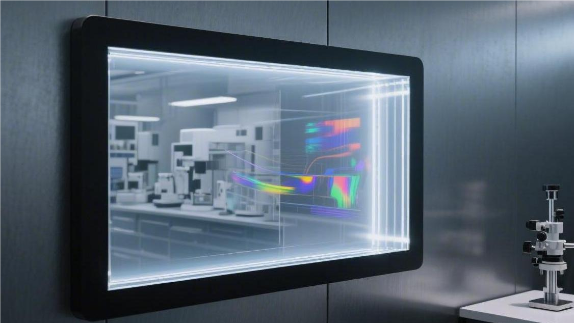
Transparent OLED has a transmittance rate of 38%-50% and a peak brightness of about 600 nits. It drives the pixels to self-illuminate through transparent electrodes. In AR applications, it controls...
댓글 남기기
이 사이트는 hCaptcha에 의해 보호되며, hCaptcha의 개인 정보 보호 정책 과 서비스 약관 이 적용됩니다.