


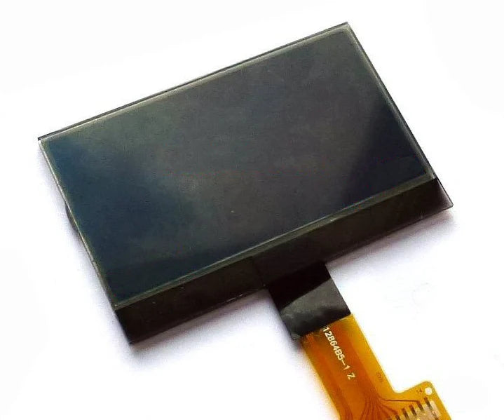
How Does COG LCD Works | Structure, Bonding Process
COG (Chip-On-Glass) technology utilizes Anisotropic Conductive Film (ACF) to directly bond driver ICs onto the LCD glass substrate through thermal ultrasonic or heat-pressure processes.
The core of the process lies in high-temperature hot pressing at 150-200°C, which enables point-to-point conduction of the conductive particles within the ACF.
Compared to traditional processes, COG can reduce packaging space by approximately 30%.
It features low power consumption, high reliability, and lower production costs, making it the industrial choice for narrow-bezel and high-resolution displays.
Structure
The COG structure directly presses the driver IC onto the Array platform of the TFT glass via the ACF medium.
Typical IC thickness ranges from 0.2mm to 0.4mm, with pin pitch reduced to the 20-micrometer level.
This solution eliminates the traditional COF (Chip-on-Film) carrier board, reducing signal transmission impedance by about 20%, while controlling the display module's bezel width to below 1.5mm, supporting the signal drive for high-PPI screens.
Glass Substrate Specifications
The substrates commonly used in industrial production are mostly alkali-free aluminosilicate glass.
Its chemical composition excludes alkali metal ions such as sodium and potassium to prevent charge migration from interfering with the electrical performance of TFT devices.
The density of this glass is typically between 2.4 and 2.5 grams per cubic centimeter.
The Coefficient of Thermal Expansion (CTE) of the substrate is the underlying logic for achieving a stable connection.
Since the CTE of the silicon material in the driver chip is approximately 2.6 ppm/°C, the CTE of the glass substrate must be controlled between 3.2 and 3.8 ppm/°C.
This minute numerical deviation is intended to compensate for the expansion and contraction displacement difference between the chip and the glass during the high-temperature hot pressing process at 180 to 220 degrees Celsius.
If the CTE matching is unbalanced, after cooling from the hot press, the conductive particles inside the ACF will shift due to shear stress, causing the pin contact resistance to soar from less than 1 ohm to hundreds of ohms, or even resulting in an open circuit.
Standard thickness has evolved from 0.7 mm in the early stages to the mainstream 0.5 mm and 0.4 mm.
In high-end ultra-thin mobile devices, the substrate thickness can be further compressed to 0.2 mm or 0.1 mm through hydrofluoric acid (HF) chemical thinning processes.
The requirements for glass surface flatness are extremely high, with flatness deviation in the center area usually required to be less than 20 micrometers, and the arithmetic mean roughness (Ra) of local areas must be lower than 0.5 nanometers.
| Physical & Electrical Parameters | Industrial Standard Specifications | Application Environment Description |
|---|---|---|
| Young's Modulus | 70 to 80 GPa | Determines the glass's ability to resist deformation during hot pressing. |
| Strain Point | Above 660°C | Ensures no permanent physical deformation occurs under high-temperature processes. |
| ITO Sheet Resistance | 10 to 100 Ω/sq | Affects the voltage drop of the drive voltage and signal response speed. |
| Conductive Layer Transmittance | 85% to 92% | Directly relates to the peak brightness and energy efficiency ratio of the display. |
| Terminal Pin Pitch | 20 µm to 50 µm | Adapts to the layout requirements of high-density pin driver chips. |
| Alignment Accuracy | Within ±3 µm | Ensures effective overlapping area between gold bumps and ITO electrodes. |
Through the DC magnetron sputtering process, a conductive film with a thickness of approximately 1000 Å to 1500 Å (100 to 150 nm) is deposited on the glass surface.
In the COG bonding area, the design of ITO terminals must consider current-carrying capacity, with a typical single pin design width of 10 to 15 micrometers.
To prevent electrochemical corrosion of ITO electrodes in humid environments, a passivation layer of Silicon Nitride (SiNx) or Silicon Oxide (SiOx) is usually covered on the surface, with a thickness of about 200 to 400 nm.
The conductive parts are exposed only at the window positions where connection with chip bumps is required through dry etching.
This multi-layer thin-film structure must possess extremely strong adhesion, with no peeling allowed in the cross-hatch test, to support the instantaneous vertical pressure of approximately 30 to 100 MPa generated during ACF hot pressing.
The lower substrate extends 2 mm to 5 mm wider than the upper substrate for mounting driver ICs and FPCs.
In this area, the cleanliness of the glass surface is a critical variable restricting bonding strength.
Before the bonding process, the glass must undergo dual-wavelength UV cleaning at 185 nm and 254 nm or oxygen plasma treatment to reduce the water droplet contact angle on the glass surface from over 40 degrees to below 10 degrees.
This treatment removes residual organic contaminants and increases surface wettability, allowing the ACF resin to form stronger covalent bonds with the glass within the flow channels.
If surface tension is insufficient, moisture will penetrate along the glass interface during subsequent reliability tests (such as the 85°C/85% RH test), leading to resin swelling and electrode oxidation.
Chip Pin Characteristics
Gold with a purity of 99.99% is selected as the pin material, primarily utilizing its extremely high chemical stability and excellent ductility to ensure that contact resistance does not rise due to oxidation over long-term use.
The hardness of the gold bumps is usually controlled between 40 and 80 HV (Vickers Hardness), which is a balanced range.
If the hardness is lower than 30 HV, the bumps will undergo excessive plastic deformation during the hot pressing process, causing the ACF adhesive material squeezed between adjacent pins to carry conductive particles and shift laterally, triggering a short circuit.
If the hardness is higher than 100 HV, the enormous pressure (usually 30 to 100 MPa) during hot pressing will be transmitted through the conductive particles to the underlying TFT glass, potentially causing micrometer-level cracks in the glass substrate.
In mainstream high-definition displays, the height standard for gold bumps is usually set at 9 micrometers to 15 micrometers.
To ensure connection reliability, the height deviation (Coplanarity) of thousands of bumps on the same chip must be strictly limited to within ±1 micrometer.
This extremely high flatness ensures that each pin can uniformly capture 3 to 5 ACF conductive particles when the hot pressing head descends.
"The flatness deviation of the pin surface must be controlled within 1 micrometer to ensure consistency in electrical connection."
| Pin Physical Parameter Item | Typical Specification Value | Industrial Precision Requirement |
|---|---|---|
| Bump Height | 9 to 15 µm | Deviation < 1 µm |
| Bump Width | 10 to 20 µm | Deviation < 0.5 µm |
| Pin Pitch | 20 to 50 µm | Cumulative tolerance < 0.2 µm |
| Single Bump Resistance | < 0.5 Ω | Stability fluctuation < 10% |
| Shear Strength | > 50 MPa | Ensures physical fixation firmness |
| Passivation Window Size | 8 µm x 8 µm | Adapts to ultra-fine pitch layouts |
In 4K or 8K high-resolution screens, due to the surge in the number of drive channels, the length of the chip edge is no longer sufficient to carry thousands of pins.
By using staggered arrangements, the effective pin pitch can be reduced from 50 micrometers to about 20 micrometers.
Under such extremely fine pitch, the aspect ratio design of the pins becomes particularly important.
Typically, the length of a rectangular pin is designed to be 50 to 100 micrometers, while the width is only 10 to 15 micrometers.
This structure not only increases the overlapping area with the glass terminals and improves mechanical strength but also provides better flow effects for the ACF adhesive, reducing bubble residue.
The current-carrying capacity of a single pin is usually designed to be around 50 mA, which fully satisfies the electric field drive signal required for liquid crystal molecular deflection while ensuring no excessive heat loss occurs under high-frequency signal transmission.
In an ideal pressing state, the contact resistance of a single gold bump through the path formed by ACF conductive particles should be stabilized between 0.3 and 0.8 ohms.
If the resistance exceeds 2 ohms, the signal will produce a significant voltage drop during transmission, leading to uneven brightness or color distortion on the screen.
"Low contact resistance is the basis for maintaining signal integrity, usually requiring stability below 1 ohm."
After bonding, the binding force between the chip pins and the glass must be verified through a Shear Test, with the standard usually requiring each bump to withstand a thrust of 10 to 20 grams.
Additionally, the Taper Angle of the pin edges is usually maintained at 70 to 80 degrees.
This slight slope facilitates the exhausting and filling of the ACF resin during the pressing process, preventing the formation of stress points at the root of the pins.
For ultra-high PPI applications, Copper Pillar bumps combined with a thin top gold layer have also begun to emerge.
Compared to pure gold bumps, the copper pillar structure has a higher modulus and thermal conductivity, allowing pin height to be further reduced and improving chip heat dissipation during high-current operation.
The Young's modulus of copper is about 120 GPa, making it more resistant to deformation than gold under extreme pressure, thereby supporting denser pin layouts without the risk of lateral short circuits.
Adhesive Film Physical Performance
In a room-temperature environment, the resin manifests as a B-stage semi-cured state, with standard thickness specifications usually distributed between 10 micrometers and 25 micrometers.
Upon entering the hot pressing process, the environmental temperature climbs from room temperature to above 150 degrees Celsius within 1 to 2 seconds.
The dynamic viscosity of the resin rapidly drops from an initial high-viscosity state to about 10 Pa·s.
This extremely low-viscosity fluid state lasts for 2 to 4 seconds, ensuring the resin fully fills the tiny gaps between the driver chip pins and the glass substrate and exhausts air bubbles between interfaces before curing.
As the hot pressing temperature continues to rise and stabilizes at 180 to 210 degrees Celsius, the latent curing agent inside the adhesive film is activated, triggering a cross-linking reaction of polymer chains, converting the resin into a high-strength solid structure within 5 to 10 seconds.
The cured resin possesses a Glass Transition Temperature (Tg) of 120°C to 150°C, ensuring that the connection site does not fail due to softening when the device generates heat during operation.
| Film Thermal & Mechanical Parameter | Industrial Standard Specifications | Physical Environment Constraint |
|---|---|---|
| Initial Thickness | 10, 15, 18, 25 µm | Selected based on chip bump height. |
| Glass Transition Temp (Tg) | 120 to 150°C | Determines modulus stability at high temperatures. |
| CTE Alpha 1 | 40 to 60 ppm/°C | Expansion rate below Tg; must match glass and silicon. |
| CTE Alpha 2 | 120 to 180 ppm/°C | Expansion rate above Tg; affects thermal stress. |
| Moisture Absorption | < 1.5% | 24-hour immersion test to prevent migration. |
| Young's Modulus | 3 to 5 GPa | Maintains physical structural strength at 25°C. |
| Peel Strength | > 600 g/cm | 90-degree peel test to verify glass adhesion. |
Mainstream ACF uses polymer spheres as the inner core, covered with a metal layer through an electroless plating process.
The diameter deviation of the inner core must be strictly limited to within ±0.1 micrometers.
The metal coverage usually consists of a nickel layer approximately 50 nm thick and a gold layer of 15 to 25 nm.
The nickel layer provides structural support and preliminary conduction, while the outer gold layer utilizes its ductility to reduce contact resistance and prevent metal oxidation.
To adapt to ultra-fine pin pitches below 20 micrometers, particle diameter specifications have evolved from the early 10 micrometers to the current 3, 3.5, or 4 micrometers.
In a 1 square millimeter area of the film, the number of conductive particles is usually set between 30,000 and 100,000.
Each particle is also coated with an insulating charge layer or micro-insulating spheres of 10 to 50 nm thickness.
This design ensures that only when subjected to a vertical pressure of 30 to 100 MPa and generating 20% to 40% deformation will the insulation layer rupture to achieve vertical conduction.
In the horizontal direction, uncompressed particles maintain their complete insulating shells, keeping the insulation resistance between pins above 10^9 ohms.
| Conductive Particle Physical Parameter | Typical Numerical Specification | Technical Application Details |
|---|---|---|
| Particle Diameter | 3.0, 3.5, 4.0 µm | Selected based on pitch and bump flatness. |
| Metal Layer Thickness (Plating) | 70 to 100 nm | Composite thickness of inner nickel and outer gold. |
| Particle Distribution Density | 40k to 100k pcs/mm² | Ensures each Bump captures 3 to 5 particles. |
| Insulation Layer Thickness | 10 to 50 nm | Ensures electrical insulation in X-Y directions. |
| Recovery Rate | 30% to 60% | Ability to maintain contact pressure after release. |
| Conduction Rupture Pressure | 10 to 30 MPa | Minimum pressure to trigger insulation rupture. |
Due to the high-activity curing agents in the resin, ACF must be stored in a low-temperature freezer at -10 degrees Celsius, where the shelf life is typically 6 months.
If exposed to room temperature (25°C), the effective usage cycle of the film will rapidly shorten to 15 to 30 days.
Before use, the film needs 30 to 60 minutes of rewarming to prevent moisture condensation during hot pressing, which could cause bubbles.
Module Stacking Logic
The bottom foundation is composed of a TFT Array glass substrate with a thickness of 0.4 mm to 0.7 mm, which includes an extended platform (Ledge) of 2.5 mm to 6 mm in length.
On this platform, the driver IC is bonded in a Flip-chip manner with the circuit side facing down, and its height is typically 0.2 mm to 0.4 mm.
The gap between the IC and the glass surface is filled by the ACF cured layer, which is only 3 to 6 micrometers thick.
To prevent liquid crystal leakage and maintain Cell Gap, the upper and lower glass layers are kept apart by Photo Spacers with a diameter of 3.5 to 4.5 micrometers, with the periphery sealed by a Sealant about 0.5 mm wide.
| Stacking Layer | Material Composition | Physical Thickness Spec | Function Description |
|---|---|---|---|
| Top Polarizer | Iodine PVA film & TAC layers | 0.12 mm to 0.15 mm | Filters light polarization direction. |
| Color Filter Substrate | Alkali-free aluminosilicate glass | 0.4 mm or 0.5 mm | Provides RGB color filter matrix. |
| Liquid Crystal Layer | Biphenyl or ester LC molecules | 3.5 µm to 4.0 µm | Changes polarization via electric field. |
| TFT Array Substrate | Glass with ITO circuits | 0.4 mm to 0.7 mm | Carries pixel switches and drive pins. |
| Bottom Polarizer | High transmittance polarizer | 0.13 mm | Works with top polarizer as a light shutter. |
| Driver IC | Thinned silicon wafer | 0.3 mm typical | Provides row and column scanning signals. |
The total Z-axis height of the module is controlled between 1.2 mm and 1.8 mm .
On the lateral layout of the Ledge area, the pin arrangement logic determines signal integrity.
The signal input end of the driver IC usually connects to a Flexible Printed Circuit (FPC), while the output end is distributed on the side near the liquid crystal cell.
To achieve reliable electrical shielding, the IC surface is usually covered with a 0.1 mm to 0.2 mm layer of silicone or epoxy resin protection.
The viscosity of this coating material must be maintained between 1500 and 3000 cps to ensure complete wetting of the four sides of the IC and the edges of the ACF.
The cured protection adhesive maintains a hardness of about Shore D 80.
- Alignment Accuracy: Fitting deviation of upper and lower substrates must be below 2 micrometers.
- Pin Overlap Rate: Overlapping area ratio between IC gold bumps and glass ITO electrodes must reach over 85%.
- Protection Glue Width: Glue must exceed the IC edge by 0.3 mm to 0.5 mm to form a moisture-proof dam.
- FPC Bonding Thickness: Total thickness of the FPC reinforcement plate and glass junction is set around 0.3 mm.
- Particle Deformation: In the Z-axis direction, conductive particles must be compressed to about 60% of their original diameter.
To lead out thousands of signal lines within the extremely narrow Ledge space, the Line/Space width and pitch are often compressed to 5 micrometers x 5 micrometers.
On the edge of the COG area, a Silicon Nitride (SiNx) passivation layer of about 200 nm is also set, with etching openings only at the IC bonding window positions.
In environmental stability experiments, this stack must withstand severe temperature cycles from -40°C to 85°C.
Due to differences in the linear expansion coefficients of silicon, glass, resin, and metal, complex shear stresses are generated within the stack.
To balance this stress, the Young's modulus of the ACF must be maintained between 3 GPa and 5 GPa after curing, acting as a mechanical buffer.
During thermal expansion, the ACF layer can absorb part of the displacement, preventing the gold bumps from detaching from the ITO electrodes.
In an 85% humidity environment, the lateral seal structure can reduce the Water Vapor Transmission Rate (WVTR) to the level of 0.01 g/m²/day.
Bonding Process
COG bonding relies on ACF (Anisotropic Conductive Film) to establish electrical paths between LCD glass ITO terminals and the driver IC.
Standard processes at 170-210°C, combined with 50-100 MPa pressure, cause 3.5-micrometer diameter conductive particles in the ACF to undergo 30%-50% plastic deformation.
Alignment tolerance must be strictly controlled within ±3 micrometers, with single-point contact resistance maintained at 1-5 ohms, supporting high-density signal transmission of over 400 pixels per inch.
Cleaning and Pre-bonding
Since glass absorbs organic molecules from the environment during storage and transport, the surface is usually covered with a hydrocarbon contamination layer about 2 to 5 nm thick.
These contaminants reduce surface energy to 30-40 mN/m, leading to poor wettability of the subsequent ACF film.
To solve this, production lines are usually equipped with UV Ozone cleaning systems.
This system uses 184.9 nm and 253.7 nm UV light to irradiate air, producing high concentrations of atomic oxygen and ozone.
Atomic oxygen is highly oxidative and can break organic molecular bonds within 30-60 seconds, converting them into CO2 and water vapor.
After treatment, the deionized water Contact Angle on the glass surface must be reduced from over 60 degrees to below 8 degrees, with surface energy increasing to above 70 mN/m.
This high-energy state facilitates rapid spreading of ACF resin during pressing, ensuring a peel strength of over 5 N/cm.
In addition to photochemical cleaning, some high-resolution lines include a Plasma cleaning process.
By introducing argon (Ar) or oxygen (O2) at 20-50 sccm into a vacuum chamber and driving glow discharge with a 13.56 MHz RF power supply, high-energy ions bombard the ITO surface at 200-500 eV to thoroughly remove stubborn inorganic particles.
- UV Lamp Power: Usually set between 20 and 30 mW/cm².
- Processing Height: Lamp distance from the glass surface is maintained at 5-10 mm.
- Cleanliness Monitoring: Particle count at sampling points must comply with Class 100 standards.
- Static Control: Glass surface charge must be neutralized to within ±50V using ion blowers.
ACF is an epoxy resin film containing a latent curing agent, with conductive particles of 3.0 to 4.0 micrometers diameter evenly distributed inside.
Due to its thermosensitivity, ACF must be stored in a freezer at -5 to -10°C.
Before use, it must be rewarmed at room temperature for 2-4 hours to prevent moisture condensation.
Pre-bonding is performed by a precision tape feeding mechanism.
The pre-bonding head is usually coated with Teflon. Parameters are set at 60-90°C, pressure at 0.1-0.4 MPa, for 1-2 seconds.
The cutter assembly cuts the ACF to match the driver IC length with a downward height accuracy of 0.01 mm to avoid damaging the glass.
The cut ACF width is usually 0.2-0.4 mm wider than the IC to allow for resin overflow during main pressing.
- ACF Width: Commonly 1.5 mm, 2.0 mm, or 2.5 mm.
- Placement Accuracy: Centerline offset must be less than 0.1 mm.
- Tension Control: Supply shaft tension is set at 0.5-1.5 N.
- Environmental Humidity: Workshop humidity is strictly controlled at 45%-55%.
If bubbles exceed 20% of the film width or long fiber-like foreign objects are found, the system alarms and rejects the substrate.
Any minor defects captured in pre-bonding will be magnified under high pressure in the main pressing stage, preventing conductive particles from forming stable mechanical contact with gold bumps.
High-quality pre-bonding is characterized by a flat, wrinkle-free ACF film with neat edges and no visible gaps with the glass substrate.
Visual Automatic Alignment
The hardware side typically uses 5MP to 12MP global shutter CCD sensors with a single pixel size of about 3.45 µm.
Combined with 1.0x to 2.0x double-sided telecentric lenses, the system eliminates parallax effects caused by depth of field fluctuations, ensuring image distortion is below 0.1% within a 0.5 mm focus range.
To accurately capture gold bumps on the driver IC and ITO Marks on the glass, a 625 nm red coaxial light source is used.
Data is transmitted via GigE or Camera Link protocols, completing sub-pixel extraction algorithms within 100 ms.
| Component Type | Performance Specification | Measurement Index |
|---|---|---|
| Camera Sensor | 2/3 inch global shutter CCD | 2448 x 2048 pixels |
| Telecentric Lens | Object-side telecentric design | Distortion < 0.05% |
| Visual Accuracy | Sub-pixel edge extraction | 1/10 pixel resolution |
| Alignment Cycle Time | Single IC recognition + movement | 0.8 to 1.2 seconds |
| Light Intensity | 10-level adjustable constant current | Above 100,000 Lux |
Gold bumps on driver ICs are usually 15 µm x 80 µm with pitches as narrow as 30 µm. Algorithms locate the geometric center of bumps in 256 grayscale levels.
Simultaneously, the upper camera aligns with L-shaped or cross-shaped Mark points on the glass.
Since ITO is nearly transparent, the light source angle is adjusted to 5-10 degrees from the normal to make outlines clear via bright-field imaging.
After obtaining center coordinates (x, y, theta) for both IC and glass, space position deviation is calculated.
To offset mechanical wear and thermal expansion, the system uses XY-Theta platforms driven by high-precision linear motors with 0.1-micrometer resolution.
Alignment accuracy (3-Sigma) must be stable within ±1.5 micrometers.
| Motion Control Item | Technical Requirement | Execution Capability |
|---|---|---|
| Platform Repeatability | Closed-loop servo feedback | +/- 0.5 µm |
| Rotation Axis Step | High sensitivity DD motor | 0.001 degree resolution |
| Guide Parallelism | Full stroke straightness | < 2 µm / 100 mm |
| Encoder Protocol | BiSS-C or Endat 2.2 | 24-bit absolute signal |
The linear expansion coefficient of glass is about 3.8 ppm/K.
In a 30°C workshop, a large panel might have a 2-5 micrometer displacement.
Visual algorithms automatically call temperature compensation models to correct target coordinates.
Simultaneously, the system features Auto Gain and Auto Exposure for different driver IC bump reflectivities.
Side View Cameras capture the parallelism between the press head and the glass; if a level difference exceeds 5 µm, the controller adjusts pressure valves to keep force fluctuation within 10%.
| Deviation Type | Cause Analysis | Control Target Range |
|---|---|---|
| Planar Displacement | Linear motor transmission error | < 1.0 µm |
| Rotation Angle | Mechanical origin drift | < 0.01 degree |
| Image Noise | Light flicker or static | SNR > 40 dB |
| Residual Error | Rounding & mechanical backlash | < 0.5 µm |
Hot Pressing Parameter Setting
The Thermal Head is usually made of ceramic or hard alloy steel, with surface flatness maintained within 2 micrometers.
Pulse Heat technology allows temperatures to rise from room temperature to 190-210°C within 1.5 seconds.
Temperature is monitored via K-type or J-type thermocouples with 1000Hz sampling, ensuring fluctuations stay within ±2°C.
Parallelism must be calibrated with Prescale paper to ensure over 90% uniformity across a 20 mm length.
Industrial standard specifications require the static calibration of parallelism for narrow-pitch driver IC pressing to ensure uniform color distribution over 90%.
Unit area pressure is set between 50 and 150 MPa.
For a 15 x 1.2 mm driver IC with 1000 gold bumps, total pressure is regulated to 60-100 Newtons.
To prevent glass damage, pressure is divided into pre-pressure (20% for 0.5-1.0s) and main pressure (switched within 0.2s).
Pressing cycles last 6-12 seconds, including heating (1-2s), constant pressure (5-8s), and cooling (2-3s).
During this time, ACF viscosity drops to 10-100 Pa·s for gap filling before cross-linking into a high-strength structure with 80-90% curing rate.
In high-PPI module production, pressure-holding time redundancy is controlled within 10% to prevent micro-cracks or thermal deformation alignment shifts.
The CTE of LCD glass (~3.8 ppm/K) and silicon (~2.6 ppm/K) creates a 4-6 micrometer size difference for a 20 mm IC at 200°C.
Visual systems pre-shrink alignment coordinates to ensure bumps hit ITO centers at target pressure.
After main pressing, a cooling system drops the head temperature to below 80°C before lifting.
This ensures the epoxy resin passes the Tg point to lock flattened particles. Particles must be compressed to 30%-50%.
If lifted too early, particles lose contact due to resin rebound, increasing resistance from 1-5 ohms to an open circuit.
Dynamic pressure monitoring curves (P-T Curve) show that residual stress at the interface must not exceed 5 N/mm² when lifting the head.
Particle Deformation Control
Usually 3.2-4.0 micrometer plastic spheres with a 0.1-0.2 micrometer gold layer.
To establish stable paths, particles must be compressed 30%-60% radially.
A standard 3.5 µm particle should reach a height of 1.8-2.2 µm, with contact resistance stabilized at 0.5-3 ohms.
- Deformation Calculation: (Initial diameter - Compressed height) / Initial diameter.
- Particle Structure: Polymer core provides elasticity; gold layer handles conduction.
- Capture Requirement: Each gold bump must capture 5 to 20 particles.
- Pressure Range: Load on a single particle must reach 50-100 mN.
Indentation marks are viewed from the glass back as quantification metrics.
Under 70 MPa, particles show a "halo" under polarized microscopes.
If deformation is <20%, contact is poor; if >70%, the polymer core breaks or the gold layer peels.
Ideal indentation diameter is 1.5-1.8x the original.
Particles must maintain a 5 µm safety margin from bump edges to prevent shorts.
99.7% of points must have resistance below 10 ohms.
- Bump Hardness: Set at HV 30 to 80 to balance "embedding" and adhesion.
- Embedding Depth: Particles should embed 0.3-0.6 µm into the gold bump.
- Height Uniformity: Bump coplanarity must be <2 µm; deformation difference <15%.
- Residual Resin: Resin layer thickness between bump and glass should be 1.0-2.0 µm.
Automated Optical Inspection (AOI) uses 520 nm green light to scan deformation.
If diameters are small, the system adds 5%-10% pressure to that area.
Systems scan 5-10 substrates per hour.
Machine stops if capture is <3 particles or deformation deviates by 20%.
Proper deformation control ensures resistance changes <50% after Dual 85 aging tests.
더 읽기
AMOLED is a pixel self-emissive technology featuring an ultra-high contrast ratio of 1,000,000:1. Black pixels do not emit light, making it more energy-efficient with more vibrant colors. It respon...
PMOLED manufacturing involves ITO patterning and organic layer evaporation. It features no TFT, relies on row and column scanning, and is suitable for small screens under 3 inches. Materials includ...
댓글 남기기
이 사이트는 hCaptcha에 의해 보호되며, hCaptcha의 개인 정보 보호 정책 과 서비스 약관 이 적용됩니다.