



How Does NexPCB Help With XR Displays
NexPCB helps XR programmes mainly at the electrical and mechanical layer: HDI and rigid-flex boards that carry display drivers, image sensors and radios inside a temple arm, plus the DFM review and pilot runs that turn a bench prototype into something a factory can build. The display is a separate purchase. The board is what makes it wearable.
The constraint is space, not speed
An XR headset has roughly a temple arm's worth of volume for everything that is not optics or battery. Inside that volume sit the display driver, a MIPI receiver, one or two cameras, an inertial sensor, a wireless radio and the power conversion for all of them. The engineering problem is fitting them without disturbing the optical stack or the wearer.
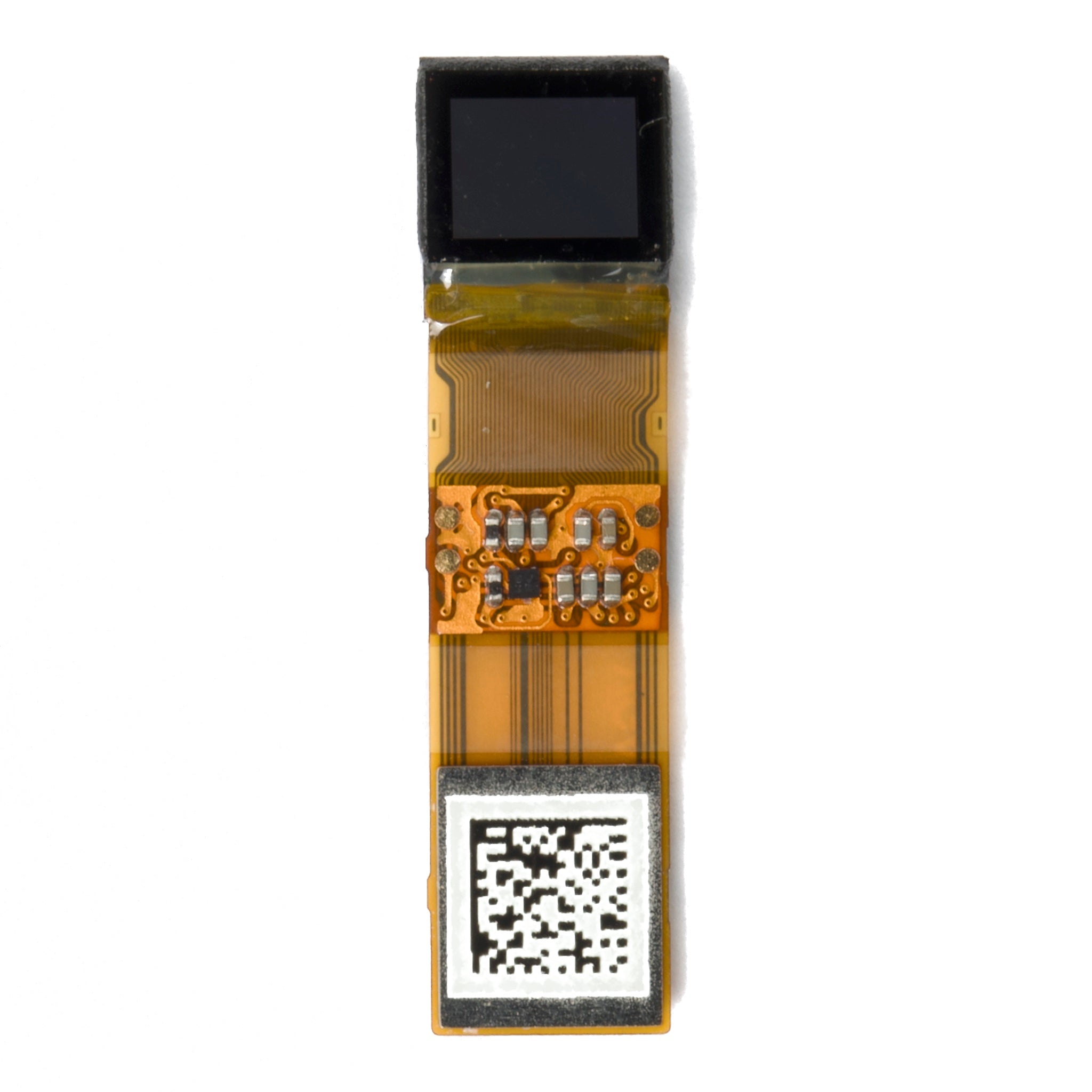
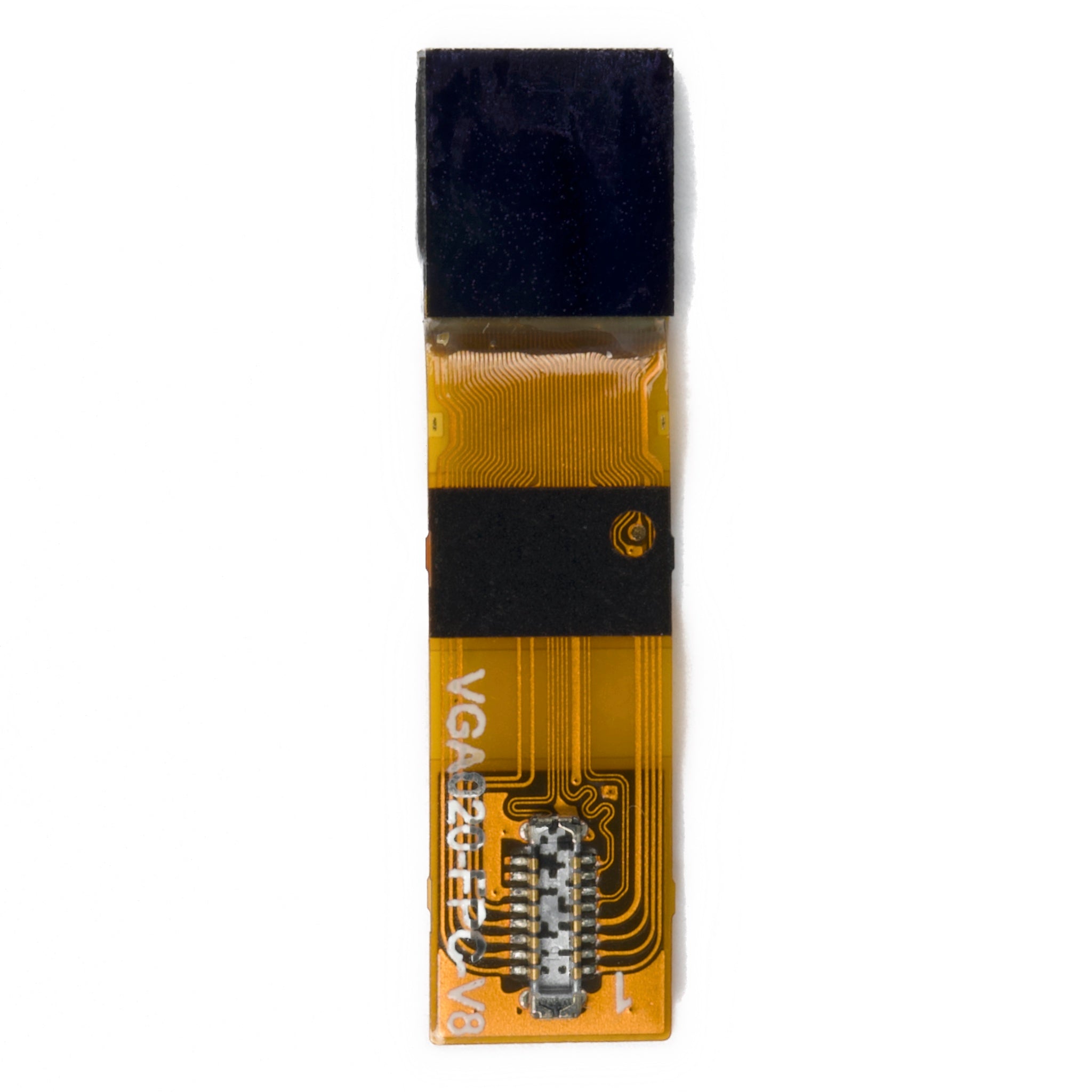
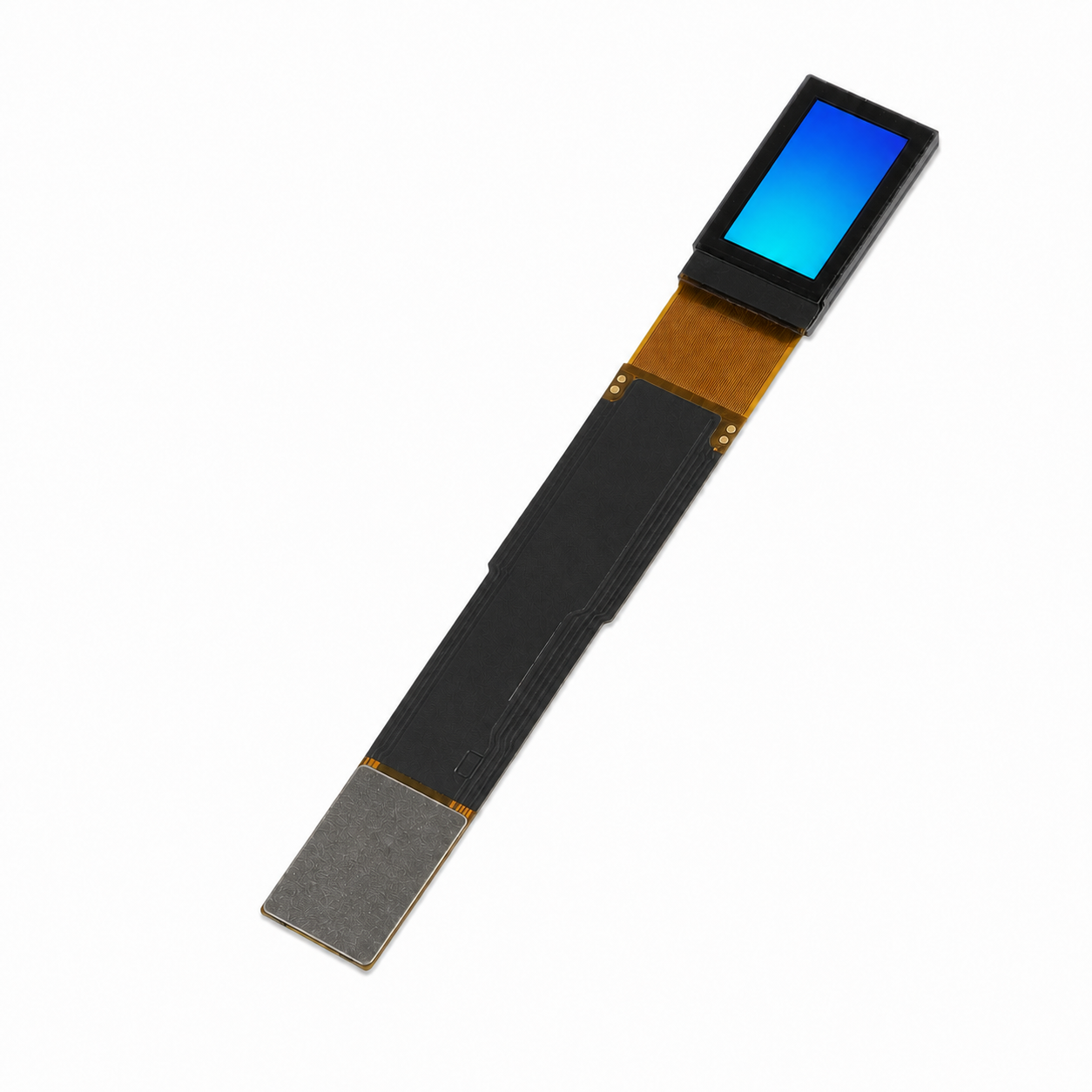
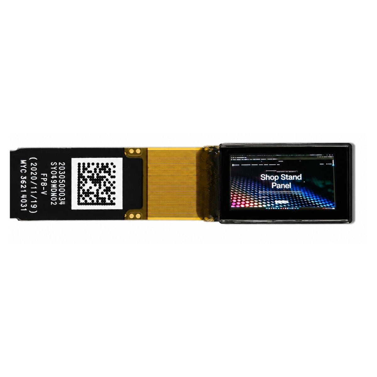
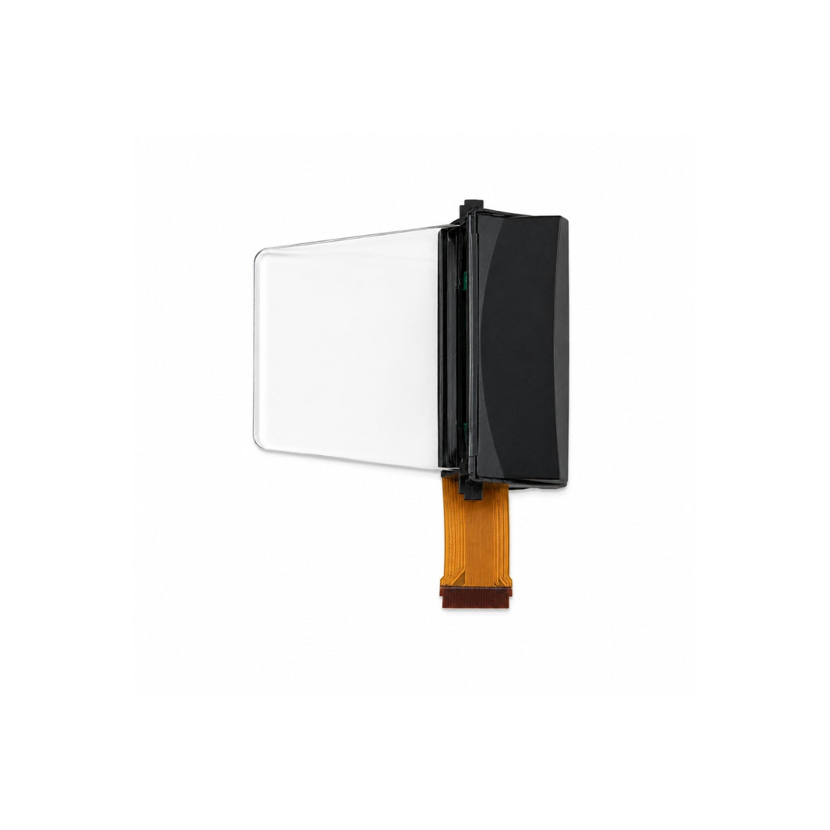
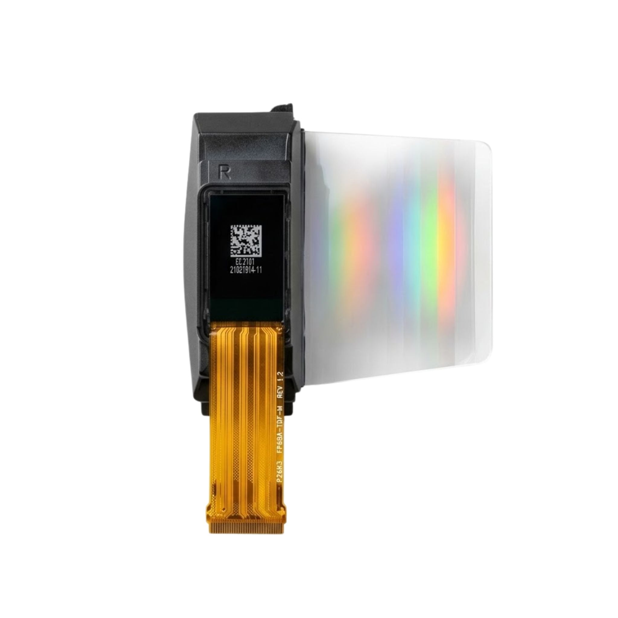
That is why board work on XR products rarely starts with a schematic. It starts with the mechanical envelope: where the panel sits, where the hinge is, how thick the arm can be, and which surfaces are allowed to get warm. The stackup follows from those answers rather than the other way round. The panel itself is chosen separately, from the micro-OLED range or from a larger AMOLED part when field of view matters more than thickness.
Rigid-flex replaces connectors
A headset bends. A rigid board does not. The conventional answer is a rigid board plus a flex cable plus two connectors, and each connector is a cost, a height and a failure mode. A rigid-flex design removes those connectors by building the flexible section into the board itself.
Four rules decide whether that works. Conductors cross the bend line at right angles rather than running along it. Vias stay out of the bend region, because a barrel is the first thing to crack. The bend radius is chosen from the finished thickness and the number of layers, not from what fits. And a stiffener is added where the flex meets a connector or a component, so the transition is not the weak point.
Static and dynamic bends are different requirements. A flex folded once during assembly can be specified more aggressively than a hinge flex that moves every time the headset is worn, and treating the two as one design produces failures that only appear after months of use.
HDI for fine-pitch drivers
Display driver packages have moved to fine pitch and small ball counts, which pushes boards toward higher density rather than more layers. HDI answers that with laser-drilled microvias, via-in-pad, and finer trace and space rules than a conventional multilayer board allows.
Two decisions dominate cost. Stacked microvias allow denser routing than staggered ones and cost more per layer pair. Via-in-pad with filled and capped vias removes the dog-bone escape that otherwise consumes space around a fine-pitch package. Both are worth it when the pitch demands it, and waste when it does not.
Assembly matters as much as fabrication. A fine-pitch package needs a stencil, paste deposit and reflow profile built for it, plus inspection that can see under the part. Asking whether the assembly house can inspect what it builds is more useful than asking its finest pitch.
Signal integrity on the display link
The display link is the part of an XR board most likely to be designed by habit rather than by analysis. MIPI DSI runs as differential pairs at rates high enough that the routing is a transmission line, which brings three requirements: controlled impedance through the whole path, matched lengths within each pair, and an uninterrupted reference plane beneath it.
The reference plane is where designs fail quietly. A pair that crosses a plane split, or passes through a region where the ground plane was cut to clear a connector, produces a reflection that may not stop the picture but will surface later as occasional corruption or as radiated emissions.
Higher lane rates cut the number of traces through the hinge but raise the energy in each one, so the same layout error radiates further. Camera links behave the same way, and a display link routed beside a camera link is a coupling path worth avoiding in the floorplan rather than patching afterwards.
Heat near the panel
Two heat sources sit close together in a headset: the display and the processor driving it. Both raise the panel temperature, and panel behaviour changes with temperature — brightness and colour shift before anything fails. Warm air against the wearer's face is the second consequence, and usually the one users complain about.
Copper balancing on the driver area, thermal vias into an internal plane, and moving the power conversion away from the panel are the standard moves. The question worth asking early is where the heat is allowed to go, because a headset has no fan and only two surfaces to reject it from.
Optical alignment is a mechanical drawing
In a see-through design, the panel, the combiner and the wearer's eye form a chain, and the board is usually the datum that holds two of the three. That makes the board's mechanical tolerances part of the optical budget rather than a fabrication detail.
Three practices help. Put the alignment features into the board itself as routed or drilled datums rather than relying on connector position. Keep the panel keep-out area explicit on the drawing, including the height of every component inside it. And account for differential expansion between board and optical element across the operating range, since a bond aligned at room temperature can shift on a cold morning.
Decide early whether alignment is fixed at assembly or adjusted per unit. Adjustment costs production time but tolerates looser board tolerance.
What to put in a quote request
Board quotations for XR work are only comparable when the request specifies the same things. Six items remove most of the ambiguity:
- Stackup and layer count, with the finished thickness the enclosure allows.
- Impedance targets for the display and camera links, and the tolerance you will accept.
- Minimum via and trace geometry, stated as a requirement rather than left to the supplier.
- Surface finish, since fine-pitch assembly and repeated flexing pull in different directions.
- Assembly scope, including which side is populated and whether test is included.
- Volume and qualification, because both change the process the supplier chooses.
A request that omits any of these will produce quotes that differ by more than the suppliers do.
From prototype to pilot
The transition that decides a programme's schedule is not the first board, it is the first thousand. Three steps make it uneventful: a DFM review before tooling covering pad geometry, solder mask dams, panelisation and assembly clearance; a pilot run built on production rather than prototype tooling; and a first-article inspection that records what was measured, so later drift is visible.
Panelisation belongs in that review too: more boards per panel lowers unit cost and raises the risk that one assembly defect wastes more material.
What a board partner does not solve
A PCB and assembly partner controls fabrication, stackup, assembly and test. It does not choose your panel, design your optics, write your firmware or certify your product. Those remain with the product team, and confusing the two leads to a schedule where the board is ready and nothing else is.
The panel decision belongs with whoever owns the AR and VR display specification, because resolution, pixel density and panel type set the link you then have to route.
Evaluating the panel
Judging a display in a headset means judging luminance, uniformity and angular behaviour under the conditions of use. ISO 9241-307 provides the analysis and compliance test methods for that, referring to the measurement procedures of ISO 9241-305.[1] None of it substitutes for the optical design, but it makes the comparison between two candidate panels meaningful.
XR panels inherit their manufacturing base from the thin-film transistor and liquid crystal work that produced laptop and television panels, with OLED arriving through a parallel chemistry route.[2] That is why small high-density panels exist at all.

XR board design is a mechanical problem with an electrical solution. Fix the envelope, decide where the flex bends, route the display link as a transmission line, and keep heat away from the panel. NexPCB's role in that chain is the fabrication and assembly that turns those decisions into a buildable board.
References
- ISO 9241-307:2008 — Ergonomics of human-system interaction — Part 307: Analysis and compliance test methods for electronic visual displays. International Organization for Standardization. https://www.iso.org/standard/40102.html
- Hilsum, C. (2010). Flat-panel electronic displays: a triumph of physics, chemistry and engineering. Philosophical Transactions of the Royal Society A, 368(1914), 1027–1082. https://doi.org/10.1098/rsta.2009.0247
더 읽기
To use a standard adapter with displays, start by aligning its input/output ports with your device (e.g., HDMI from laptop) and display (e.g.
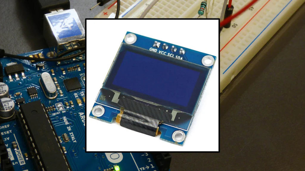
To install a PMOLED module correctly, start by wearing anti-static gloves to prevent damage, then clean the PCB surface with 99% isopropyl alcohol on a.
댓글 남기기
이 사이트는 hCaptcha에 의해 보호되며, hCaptcha의 개인 정보 보호 정책 과 서비스 약관 이 적용됩니다.