


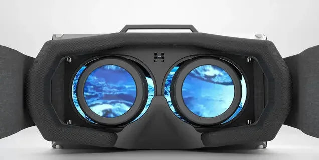
Micro OLED Displays for AR/VR | Key Specs, Performance
Micro OLED features 3000+ PPI and 5000 nit brightness, completely eliminating the screen-door effect;
The 0.01 ms ultra-fast response time solves motion sickness, serving as the performance benchmark for achieving lightweight AR/VR and 4K ultra-clear image quality.
Key Specs
Micro OLED utilizes a monocrystalline silicon backplane to achieve a PPI of over 3500, far exceeding the 800 PPI of traditional glass substrates.
Currently, the resolution of a 1.3-inch panel reaches 3840 by 3552.
By employing a tandem structure, brightness can be increased from 1500 nits to 5000 nits, with a contrast ratio exceeding 100,000:1.
The response speed is controlled within 10 microseconds, supporting a 120 Hz refresh rate.
These parameters meet the requirements of devices like Apple Vision Pro for high PPD (Pixels Per Degree) and low latency.
Pixels & Clarity
Micro OLED technology builds display pixels on 12-inch monocrystalline silicon wafers, using semiconductor lithography processes to replace the Fine Metal Mask (FMM) process used on traditional glass substrates.
This manufacturing path allows the pixel pitch to shrink to between 4 micrometers and 9 micrometers, integrating over 13 million independent light-emitting points within a 1.3-inch display area.
Compared to the PPI of approximately 460 to 550 for high-end smartphones, Micro OLED achieves a PPI increase to 3500–4500.
This high-density physical arrangement allows near-eye display devices to maintain smooth image edges even after more than 10x optical magnification.
In actual hardware tests, the resolution of a 1.3-inch panel reaches 3840 by 3552, with a physical pixel count more than six times that of a traditional 1080P panel.
| Technology Category | Substrate Material | Pixel Pitch | Pixel Density (PPI) | Transistor Technology |
|---|---|---|---|---|
| Traditional LCD | Glass | 45 to 65 µm | 400 to 800 | a-Si / LTPS |
| Mobile OLED | Flexible Polyimide | 30 to 50 µm | 450 to 600 | LTPS / LTPO |
| Micro OLED | Monocrystalline Silicon | 4 to 8.5 µm | 3000 to 4500 | Monocrystalline Silicon CMOS |
The limit of human retinal resolution is approximately 60 pixels per degree (60 PPD).
When using optical lenses with a 100-degree Field of View (FOV), the PPD of traditional headsets is typically only between 15 and 25, causing users to perceive black gaps between pixels.
By increasing the total pixel count, Micro OLED can provide 40 to 60 PPD within the same 100-degree FOV, eliminating this grid effect.
This image performance stems from the high aperture ratio under the CMOS process, which is the proportion of the light-emitting area to the total pixel area.
The aperture ratio of Micro OLED is typically maintained above 80%, whereas traditional technologies often have an aperture ratio of only about 50% due to wiring occupying space.
| Display Indicator | 0.7-inch Panel | 1.3-inch Panel | Future Standard (Expected) |
|---|---|---|---|
| Single Eye Resolution | 1920 by 1080 | 3840 by 3552 | 4096 by 4096 |
| Pixel Size | 8.1 µm | 7.4 µm | 6.3 µm |
| Screen Ratio | 16:9 | 1.08:1 | 1:1 |
| Theoretical PPI | 3147 | 3400 | 4032 |
On monocrystalline silicon wafers, electron mobility is much higher than on polycrystalline silicon on glass substrates.
High mobility allows transistor sizes to be extremely small while maintaining extremely high switching speeds.
The current mainstream White OLED plus Color Filter (WOLED+CF) architecture achieves color display by covering a white light-emitting layer with a nanometer-scale layer of red, green, and blue filters.
Each set of RGB sub-pixels is only 2 to 3 micrometers wide.
To further improve brightness and clarity, some manufacturers like Kopin or Sony are advancing Direct Patterned OLED technology, which eliminates color filters and allows sub-pixels to emit light independently.
This technical path can increase light utilization by more than 2 times, corresponding to the possibility of achieving higher sensory clarity at lower power consumption.
Micro OLED generally adopts a standard RGB stripe arrangement rather than the PenTile arrangement common in smartphones.
Standard arrangement avoids color edge interference when rendering fine text or diagonal lines.
In spatial computing scenarios, users' demand for reading virtual documents requires extremely high sharpness of text edges.
Tests show that 4000 PPI Micro OLED can clearly present the strokes of size 4 font edges without producing any blurring.
| Visual Evaluation Item | Traditional VR (LCD) | High-end VR (AMOLED) | Micro OLED Performance |
|---|---|---|---|
| Screen-door Effect Perception | Clearly visible | Relatively obvious | Completely unidentifiable |
| Dotted Edge Smoothness | Stepped feeling | Jagged | Smooth as a photograph |
| Text Reading Clarity | Limited to large titles | Barely readable body text | Supports long-term document reading |
| Image Color Purity | Medium | High | Extremely High (Lithography-grade alignment) |
When headsets adopt Pancake folded optical lenses, the increase in optical path length places higher requirements on the original resolution of the display panel.
The 12 million pixels provided by the 1.3-inch panel are distributed more uniformly across the user's field of view after lens magnification.
The width of the black area between pixels is compressed to less than 1 micrometer, which is physically close to the diffraction limit of visible light.
A single 12-inch silicon wafer can be cut into dozens of 1.3-inch display modules.
The pixel yield of each module needs to be screened through Automated Optical Inspection (AOI).
Because pixels are extremely small, any tiny dust particle can cause a dead pixel; therefore, the production environment requires an ISO Class 1 ultra-clean room.
This nearly clinical manufacturing standard ensures that screens delivered to users have extremely high pixel consistency at 4K resolution.
Panel non-uniformity (Mura) is controlled within 1%, ensuring that when displaying pure color backgrounds, no cloud-like patches appear, enhancing transparency and clarity from a visual perspective.
Brightness & Contrast
On 12-inch silicon substrates, the current mainstream dual-stack (tandem) architecture achieves doubled brightness under the same current density by vertically stacking two sets of organic light-emitting layers.
Laboratory data shows that 1.3-inch panels using this structure can maintain a peak brightness between 5000 nits and 10,000 nits.
Since AR or VR devices generally use Pancake folded optics, light loses about 85% to 90% of its energy during multiple refractions and reflections.
To ensure that the brightness reaching the user's eye remains at a comfortable level of over 500 nits, the original output of the display panel must be significantly redundant.
| Parameter Category | Industrial Standard Data | Hardware Implementation Logic | Actual Visual Performance |
|---|---|---|---|
| Peak Brightness | 5000 to 12000 nits | Multi-stack light-emitting material stacking | Ensures clear images in high-light outdoor environments |
| Black Level Brightness | Below 0.0001 nits | Silicon-based CMOS completely cuts off current | Presents physically pure black |
| Static Contrast Ratio | 1,000,000:1 | Pixel-level independent switch control | Deep images with no light leakage |
| Brightness Uniformity | Over 98% | Wafer-level process error control | Consistent full-screen brightness, no shadow spots |
To reduce visual persistence (motion blur) caused by eye movement, the panel is typically only turned on and emitting light for 10% to 20% of each frame cycle.
At a 120 Hz refresh rate, the actual pixel lighting time is only about 1 millisecond.
This means if a panel's nominal brightness is 5000 nits, after enabling Low Persistence mode, its effective sensory brightness will decay to 500–1000 nits.
To counter this, manufacturers add a Micro Lens Array (MLA) above the color filters to refocus light that would otherwise scatter sideways, increasing light extraction efficiency by more than 30%.
- Contrast Control Logic: The transistor leakage current of the silicon-based backplane is extremely low, allowing the brightness of non-emitting pixels to be suppressed below the limit of human perception.
- HDR Performance Data: Supports 10-bit or even 12-bit grayscale control, presenting over 1024 levels of detail layering when displaying the span from 0.0001 nits to 5000 nits.
- AR Transparency Matching: In AR devices, contrast determines the fusion quality of virtual objects with real backgrounds; high contrast eliminates the "cheap" feeling of semi-transparent shadows.
- Power Consumption Balance: Although brightness is extremely high, thanks to the high electron mobility of monocrystalline silicon, the current loss per 1000 nits of brightness is about 40% lower than traditional displays.
Traditional LCD panels, even with Local Dimming, still suffer from halo effects that cause dark backgrounds to appear grayish.
The self-emissive nature of Micro OLED ensures that every 4-micrometer pixel is an independent light control unit.
When users observe starry skies or deep-sea scenes in virtual reality, there is no light bleed around the stars against the black background.
When measuring instruments detect a full black signal, the ammeter reading is nearly zero; this ultimate light control capability is the physical foundation for achieving High Dynamic Range (HDR) video display.
For AAA-level VR games, high contrast enhances the sense of layering in light and shadow, making shadows produced by virtual light sources more consistent with the physical characteristics of the real world.
| Solution Comparison | Brightness Potential | Contrast Depth | Energy Conversion Rate | Applicable Optical Path |
|---|---|---|---|---|
| Single-layer WOLED | 1000 to 1500 nits | 1,000,000:1 | Medium | Fresnel Lens |
| Dual-stack WOLED | 3000 to 6000 nits | 1,000,000:1 | High | Pancake Lens |
| Direct Patterned RGB | Above 8000 nits | 1,000,000:1 | Extremely High | AR Diffraction Waveguide |
For AR diffraction waveguide devices, ambient light is often as high as tens of thousands of nits, which requires Micro OLED brightness to be extremely competitive.
In scenarios with direct noon sunlight, ambient brightness can reach 30,000 nits; if the display brightness is insufficient, virtual information will be completely obscured.
Current advanced monocrystalline silicon backplanes, combined with special high-gain materials, can push the excitation power of a single pixel to the limit.
On 0.7-inch small-size panels, overall brightness performance can be pushed higher by optimizing the arrangement ratio of red, green, and blue sub-pixels while maintaining color balance.
Some products have already achieved an explosive output of 15,000 nits brightness in a very short time to meet instantaneous strong light environment requirements.
A 1.3-inch Micro OLED running a full white screen at a full load of 5000 nits typically maintains power consumption within 2 watts.
Silicon materials themselves have excellent thermal conductivity, allowing heat generated by pixels to be quickly conducted to the metal frame of the headset.
This thermal performance avoids performance degradation of organic materials caused by excessive temperature, ensuring that the brightness decay curve remains flat over thousands of hours of use.
In actual long-term tests, panels using this process typically exhibit a brightness drift of less than 3% after 500 hours of continuous high-brightness operation, ensuring the consistency and stability of the long-term visual experience.
Response & Refresh Rate
On monocrystalline silicon substrates, electron migration speed is more than 100 times faster than on traditional glass substrates, allowing pixel state switching to be completed within 10 microseconds (0.01 ms).
In contrast, the response time of high-end LCD panels is typically between 2 ms and 5 ms. This physical performance difference allows Micro OLED to eliminate image ghosting when processing high-speed dynamic images.
In near-eye display environments like AR or VR, any pixel latency exceeding 1 ms will be magnified by the optical lens, leading to visual double-imaging.
Micro OLED's sub-millisecond characteristic ensures that each frame of the image can completely disappear and reset before the next frame signal arrives, maintaining extremely high dynamic clarity.
"Pixel switching is completed in microseconds, which is several times faster than the limit of human visual perception."
| Display Technology | Typical Response Time | Refresh Rate Upper Limit | Drive Method |
|---|---|---|---|
| Traditional LCD | 2 to 8 ms | 144 Hz | Rolling Scan |
| Mobile AMOLED | 0.5 to 1 ms | 120 Hz | Rolling Scan |
| Micro OLED | Below 0.01 ms | 120 to 240 Hz | Global Scan |
Currently, mainstream 1.3-inch Micro OLED panels support switching modes of 90 Hz, 100 Hz, and 120 Hz. In 120 Hz mode, the display period of each frame is only 8.33 ms.
The silicon-based backplane receives video streams through high-speed data interfaces (such as MIPI or DisplayPort) and utilizes integrated SRAM storage units to achieve precise control of pixel voltage.
When users rotate their heads quickly, high refresh rates increase image sampling density, making the movement trajectory of virtual objects in the field of view smoother.
Laboratory tests show that when the refresh rate is increased from 60 Hz to 120 Hz, user-observed motion discontinuity is reduced by approximately 50%.
"A frame update speed of 120 times per second is a basic requirement for achieving immersion in spatial computing devices."
By controlling the duty cycle, the panel only lights up pixels for about 1 ms to 2 ms within the 8.33 ms frame period, remaining black for the rest of the time.
In traditional displays, pixels emit light continuously throughout the frame cycle; when the eye moves, the image shifts position on the retina, creating a sense of blur.
Micro OLED's extremely short response time allows the system to complete pulsed lighting within an extremely short window.
Data shows that when the duty cycle is reduced to below 15%, dynamic blur can be compressed to a level imperceptible to the human eye, keeping dashboard digits sharp even in high-speed racing simulation applications.
| Refresh Rate Setting | Frame Period Time | Recommended Duty Cycle | Dynamic Blur (Pixels) |
|---|---|---|---|
| 60 Hz | 16.67 ms | 20% | Relatively obvious |
| 90 Hz | 11.11 ms | 15% | Slight |
| 120 Hz | 8.33 ms | 10% to 12% | Extremely Low |
Motion-to-Photon Latency is a comprehensive indicator for evaluating AR/VR performance, and the drive architecture of Micro OLED significantly shortens this path.
Since the drive circuitry is directly integrated onto the display backplane, the internal processing latency from signal reception to pixel excitation is typically below 1 ms.
Combined with high-performance sensors and algorithms, the total system latency can be controlled within 20 ms.
"The global pixel update mechanism ensures real-time alignment of physical image position with sensor data."
- Electron Mobility Performance: The mobility of monocrystalline silicon transistors exceeds 500 cm²/Vs, supporting nanosecond-level current switching.
- Synchronization Performance Data: The panel supports frame synchronization with external cameras, with the error range controlled within 100 microseconds.
- Multi-frequency Compatibility: Capable of seamlessly switching between 24 Hz, 60 Hz, and 120 Hz to adapt to the frequency requirements of movie playback and high-performance gaming.
- Afterglow Control: The brightness decay time after extinguishing is extremely short, preventing residual charge interference for the next frame.
Under high-refresh-rate operation, Micro OLED power consumption performance has a linear relationship with pixel flip speed.
Because the parasitic capacitance of the monocrystalline silicon backplane is extremely small, heat generated by frequent level switching is kept at a low level.
A 1.3-inch panel running at full load at 120 Hz typically sees an increase in logic drive power consumption of no more than 200 mW.
Performance
This technology achieves pixel densities of 3000 to 4500 PPI on panels under 1.3 inches, with single pixel size shrinking to 4 to 9 micrometers.
Its switching response speed is below 0.01 ms, and the contrast ratio exceeds 100,000:1.
At a 120 Hz refresh rate, motion blur almost disappears.
Brightness ranges from 1000 to 5000 nits, with over 95% DCI-P3 color gamut coverage, providing extremely high visual analytical power for AR/VR.
Pixel Density Performance
Currently, the physical resolution of mainstream 0.7-inch panels typically reaches 1920 * 1080, while 1.3-inch level panels have achieved a single-eye resolution of 3840 * 3552.
This arrangement density compresses the pixel pitch to between 4 micrometers and 9 micrometers, nearly a 10x reduction compared to traditional glass-substrate OLEDs.
The number of pixels per unit area shows exponential growth, with Pixels Per Inch (PPI) stabilizing in the range of 3000 to 4500; some laboratory prototypes have already demonstrated capabilities exceeding 6000 PPI.
| Screen Type | Typical Size (inch) | Resolution Specification | Pixel Density (PPI) | Pixel Pitch (µm) |
|---|---|---|---|---|
| High-end Mobile LCD | 6.7 | 2778 * 1284 | 450 - 500 | 50 - 55 |
| VR-specific LCD | 2.5 | 2160 * 2160 | 1000 - 1200 | 20 - 25 |
| Standard Micro OLED | 0.71 | 1920 * 1080 | 3100 | 8.2 |
| High-end Micro OLED | 1.3 | 3840 * 3552 | 4000+ | 6.3 |
The human eye's resolution limit under normal vision is about 60 PPD. Traditional VR devices, limited by LCD screens around 1000 PPI, typically have a PPD of only 20 to 25 within a 100-degree FOV.
Using 3500 PPI Micro OLED panels combined with advanced Pancake folded optical solutions, devices can easily provide 50 to 70 PPD visual clarity.
Because silicon wafers possess extremely high carrier mobility, transistors can be made very small with extremely fast switching speeds.
This 3D stacked structure gives Micro OLED a very high aperture ratio, with the light-emitting area often exceeding 90%.
In contrast, because LTPS technology on glass substrates needs to avoid metal routing, its aperture ratio is often below 50%.
High aperture ratio reduces the current load on individual pixels; at the same brightness output, the current density of each light-emitting unit is lower, slowing organic material decay and extending panel lifespan under high PPI operation.
| Technical Indicator | Silicon-based CMOS Drive | Glass-based LTPS Drive | Performance Gap |
|---|---|---|---|
| Transistor Size | < 1 µm | 3 - 5 µm | Silicon is more refined |
| Carrier Mobility | > 500 cm²/Vs | 50 - 100 cm²/Vs | Silicon is 5-10x faster |
| Wiring Layers | 5 - 10 Metal Layers | 2 - 3 Metal Layers | Silicon has higher integration |
| Pixel Alignment Accuracy | < 0.2 µm | 1 - 2 µm | Silicon is more precise |
Currently, Micro OLED mainly adopts the White OLED with Color Filter (WOLED + CF) structure.
In this solution, the white light layer is evaporated continuously across the entire surface, pixel division is defined by the underlying CMOS substrate, and color separation relies on the color filters covering the top.
Through semiconductor lithography, filter dimensions can precisely match 4-micrometer pixel units.
To further push pixel density and brightness, the industry is researching FMM-RGB (Fine Metal Mask) processes, attempting to directly evaporate red, green, and blue.
Constrained by mask physical tension and deformation, the current PPI upper limit for RGB solutions is around 1500, whereas WOLED solutions based on semiconductor lithography have already surpassed the 4000 PPI commercialization threshold.
A 4000 * 4000 resolution screen at 90 Hz refresh rate and 10-bit color depth generates an original data stream exceeding 40 Gbps per second.
The CMOS backplane integrates local storage and image processing algorithms into each pixel cluster, supporting Mobile Industry Processor Interface (MIPI) and Display Stream Compression (DSC) technology.
These circuits are directly embedded in the silicon wafer area at the display's edge, reducing the number of pins on external driver chips.
The good thermal conductivity of the silicon substrate also supports the operation of high-density pixels; monocrystalline silicon's thermal conductivity is approximately 148 W/mK, much higher than glass's 1.1 W/mK.
Micro OLED adds a Micro Lens Array (MLA) above the color filter layer.
Each micro lens is precisely aligned with the sub-pixel below it, converging light that would otherwise diverge sideways into a vertical direction.
This optical layer increases axial brightness by 50% to 100% without increasing power consumption.
At a microscopic scale of 3500 PPI, the micro lens diameter is only a few micrometers, and its manufacturing difficulty is comparable to wafer production.
This highly integrated optical and semiconductor structure allows Micro OLED to achieve extremely high pixel density while maintaining a peak brightness of over 3000 nits, meeting HDR10 display standards.
Motion Blur Control
During the process of switching a pixel from one grayscale to another (GtG), Micro OLED's transition time is typically less than 0.01 ms.
In contrast, even for Fast-LCDs optimized for VR, the response time remains around 1 to 2 ms.
This orders-of-magnitude difference stems from different underlying physical mechanisms: LCDs require voltage to drive the physical rotation of liquid crystal molecules to change light transmittance, whereas Micro OLED is a current-driven self-emissive technology that can instantly adjust the emission intensity of organic materials by controlling current magnitude.
At 90 Hz or 120 Hz refresh rates, this microsecond-level response ensures each frame of the image reaches target brightness in a very short time, avoiding physical overlap of the previous frame's ghosting with the next frame's display.
- Response Time Comparison: Micro OLED is at the 10 microsecond level, whereas traditional displays are mostly above 1000 microseconds.
- Dynamic Transition Latency: The rising and falling edges of pixel color switching are nearly vertical, with no trailing trails in the image.
- High Frequency Refresh Support: Silicon-based CMOS drive circuitry supports internal logic refreshes up to 240 Hz or higher, adapting to high-dynamic gaming scenes.
- Image Purity: Edges of moving objects do not produce color fringing or blurry ghosting during high-speed movement.
When the user's head rotates, the image position on the retina shifts, causing the brain to perceive a blurred image.
To solve this phenomenon, Micro OLED adopts a Low Persistence mode, which significantly shortens the actual display time of each frame through Pulsed Driving.
In a typical 90 Hz working mode, one frame's total duration is approximately 11.1 ms; Micro OLED can compress the lighting time to 1 to 2 ms or even shorter, inserting black frames for the remaining time.
- Duty Cycle Adjustment Range: Supports flexible configuration from 10% to 25%, balancing brightness and clarity.
- Visual Persistence Time: The physical residence time of each frame on the retina is strictly controlled within 2 ms.
- Display Synchronization Mechanism: Pulsed lighting time is perfectly aligned with data refreshes from IMU inertial sensors.
- Brightness Compensation Technology: Compels a momentary boost in drive current to compensate for brightness loss caused by black frame insertion, maintaining peak output.
Micro OLED's CMOS backplane integrates high-speed buffers and Timing Controllers (T-CON), capable of directly processing data streams after distortion correction and chromatic aberration compensation.
This highly integrated circuit shortens the data transmission path between the Display Driver IC (DDIC) and pixels.
Currently, combined with advanced rendering algorithms, systems equipped with Micro OLED can suppress total MTP latency to below 20 ms.
- Transmission Protocol Support: Compatible with MIPI D-PHY/C-PHY interfaces, with single-channel bandwidth up to 2.5 Gbps.
- Internal Data Throughput: Processes more than 5 billion pixels per second without frame loss.
- Intra-frame Latency Control: The latency difference from top to bottom scanning is controlled at the microsecond level, supporting global-shutter-style display effects.
- Prediction Compensation Compatibility: The circuit level supports fast responses to Time Warp algorithms.
Traditional glass substrates see liquid crystal molecules become viscous in low-temperature environments, causing response times to stretch sharply to over 10 ms, leading to severe ghosting.
Due to solid-state electronic characteristics based on monocrystalline silicon, Micro OLED pixel response times remain nearly unchanged in the range of -20°C to +70°C.
This thermal stability ensures motion control capabilities in different environments.
The high thermal conductivity of the silicon substrate (148 W/mK) also prevents heat accumulation from high-frequency driving, ensuring the image remains stable at 120 Hz without frequency drops or image jitter due to overheating.
- Temperature Stability: Response speed change rate at -20°C is less than 5%.
- Heat Conduction Efficiency: Heat dissipation speed is over 100 times that of traditional glass substrates.
- High Frequency Load Capacity: Supports continuous 120 Hz operation for long periods without phase shift.
- Anti-interference Performance: CMOS circuits come with good electromagnetic shielding, ensuring signal transmission accuracy.
Brightness Output Capability
In AR/VR hardware, light efficiency loss in the optical system is an unavoidable prerequisite.
VR devices using Pancake folded optics typically lose 85% to 90% of light; if the screen outputs 3000 nits, the brightness reaching the human eye is only 300 to 450 nits.
In AR glasses using waveguide technology, light efficiency is often below 1%, placing extremely high demands on the display source's original brightness.
Currently, commercially produced Micro OLED panels can generally maintain peak brightness of 1500 to 5000 nits, while experimental prototypes in the development stage have achieved lab data exceeding 10,000 or even 15,000 nits by improving material systems.
"At a 10% duty cycle, Micro OLED needs to instantaneously generate ten times the average pulse brightness to compensate for visual brightness loss in low persistence mode."
To increase brightness without significantly increasing power consumption, Tandem OLED (multi-layer serial structure) has become the mainstream choice.
This architecture vertically stacks two or more light-emitting units via a Charge Generation Layer (CPL); under the same drive current, the brightness of a dual-layer tandem structure can reach about twice that of a single-layer structure.
Since current density is distributed across multiple emitting layers, the physical aging speed of organic materials is significantly reduced, effectively extending the panel's lifespan under high-brightness operation.
Laboratory test data shows that panels using dual-layer tandem structures typically have an operating life exceeding 30,000 hours at 1000 nits brightness.
"The thermal conductivity of the silicon substrate is about 148 W/mK, far higher than the 1.1 W/mK of glass substrates, supporting Micro OLED thermal stability under high current density."
Micro OLED integrates a layer of micro lenses manufactured via semiconductor lithography above the color filters, with each lens being only a few micrometers in diameter.
These lenses can converge light that originally scattered at large angles toward the observer's pupil, increasing light extraction efficiency by 50% to 100%.
In 3500 PPI high-density arrangements, micro lens alignment accuracy requires sub-micrometer precision.
Besides MLA technology, the Micro-cavity Effect inside the emitting layer also causes constructive interference of specific wavelengths by precisely controlling organic layer thickness, further purifying colors and strengthening forward light intensity.
"By adjusting the thickness of the micro-cavity structure, Micro OLED can increase the intensity of specific wavelengths by over 30% and significantly narrow the FWHM to improve color purity."
To eliminate motion blur, displays typically only light up for a small percentage of a frame's duration. This low duty cycle mode solves ghosting but proportionally cuts perceived brightness.
If a system is set to a 20% duty cycle, to allow the user to perceive 1000 nits, the panel must output a real intensity of 5000 nits at the moment of lighting.
The silicon-based CMOS drive backplane possesses strong instantaneous current supply capabilities to support such high-frequency pulses.
This current control precision is typically achieved by 10-bit or higher Digital-to-Analog Converters (DACs), ensuring that grayscale performance and color consistency do not drift due to violent current fluctuations at different brightness levels.
When users use the device in outdoor daylight, the ambient background brightness can reach 3000 to 10,000 nits.
If the brightness entering the eye is insufficient, virtual information will appear semi-transparent or even disappear completely.
Micro OLED, combined with local contrast enhancement algorithms, can turn off pixels when displaying black backgrounds to provide near-infinite contrast, making color images appear deeper in bright environments.
Current industry standards are evolving toward commercial shipping specs of over 4000 nits per eye to adapt to more diverse application environments.
Power Efficiency Advantages
Backplanes manufactured using 28 nm or 40 nm CMOS processes typically maintain logic circuit operating voltages around 1.8 V, much lower than the voltage required for traditional LTPS on glass substrates.
Monocrystalline silicon possesses extremely high electron mobility, significantly reducing transistor turn-on and turn-off losses.
Drive circuits under each pixel are designed with refinement, maintaining parasitic capacitance at the femtofarad (fF) level, reducing dynamic power consumption during high-frequency refreshes.
At refresh rates common in AR/VR devices, such as 90 Hz or 120 Hz, the low capacitance characteristic keeps energy dissipation during data transmission and voltage conversion extremely low.
As it is a self-emissive technology, each pixel independently controls current based on content; when displaying dark backgrounds or night scenes in VR, pixels are completely off or in an extremely low current state, with current consumption near 0 mA.
Current dual-layer Tandem structures achieve doubled brightness at the same current intensity by adding a charge generation layer between two emitting units.
From physical parameters, single-layer OLED luminous efficiency is typically 15 to 30 cd/A, whereas dual-layer tandem structures can reach 50 to 80 cd/A.
This efficiency boost not only reduces battery load but also lowers current density in organic materials under high brightness. Lower current density results in less Joule heat, slowing the material's thermal degradation process.
At a common brightness of 1000 nits, this structure allows the panel's overall power consumption to be controlled within 300 mW.
Silicon's thermal conductivity is about 148 W/mK, whereas traditional glass is only 1.1 W/mK.
Heat generated by the panel can quickly diffuse through the silicon wafer to a heat sink or metal frame.
Lower operating temperatures improve the subthreshold swing characteristics of CMOS drive transistors, reducing leakage current caused by high temperatures.
In experimental tests, when panel temperature rose from 25°C to 60°C, the increase in static power consumption for silicon-based circuits was far less than for glass-based circuits.
To eliminate motion blur, Micro OLED typically runs in Low Persistence mode, lighting up for only about 10% to 25% of each frame's time.
During black frame insertion, pixel drive current is cut off.
Although it is necessary to increase peak current at the moment of lighting to maintain sensory brightness, overall average current is still optimized.
Through refined control of nanosecond-level timing for pixel opening, the drive chip can achieve up to 1024 levels of brightness adjustment.
Micro OLED integrates the timing controller, color compensation algorithm memory, and voltage regulation modules all on the same silicon substrate.
Traditional external drive solutions generate significant signal thermal loss due to the parasitic impedance of Flexible Printed Circuits (FPCs) when transmitting 4K-level data streams.
The integrated solution limits these signal interactions to micrometer-level on-chip wiring, reducing data transmission power consumption by more than 30%.
The application of Micro Lens Arrays (MLA) converges light from pixels into a narrower angular range.
Through this physical optical gain, light that originally radiated in all directions is collected and directed toward the human pupil.
For the same perceived brightness, the drive circuit can reduce initial emission intensity by 30% to 50%.
At an ultra-high pixel density of 3500 PPI, the precision of each micro lens determines the upper limit of electro-optical conversion efficiency.
Experimental data shows that Micro OLED modules with efficient MLA structures produce 1.8 times more effective lumens per watt than traditional structures.
In VR games or high-load rendering scenarios, the temperature rise of the screen portion is typically controlled within 5 to 8 degrees Celsius.
Under the combined action of high-efficiency materials, monocrystalline silicon backplanes, and advanced optical structures, Micro OLED achieves a balance between high resolution and low energy consumption, solving the conflict between performance and battery life in mobile headsets.
By continuing to optimize CMOS drive logic and improving charge transport layer efficiency, future panels are expected to reduce operating power consumption by another 20% while maintaining existing brightness levels.
더 읽기
PMOLED manufacturing involves ITO patterning and organic layer evaporation. It features no TFT, relies on row and column scanning, and is suitable for small screens under 3 inches. Materials includ...
Micro OLED is a silicon-based OLED technology with a pixel density exceeding 3000 PPI and a brightness of several thousand nits. It is small in size, has low power consumption, and offers extremely...
댓글 남기기
이 사이트는 hCaptcha에 의해 보호되며, hCaptcha의 개인 정보 보호 정책 과 서비스 약관 이 적용됩니다.