



Micro OLED Module Technology | How It Works, Manufacturing Process, Trends
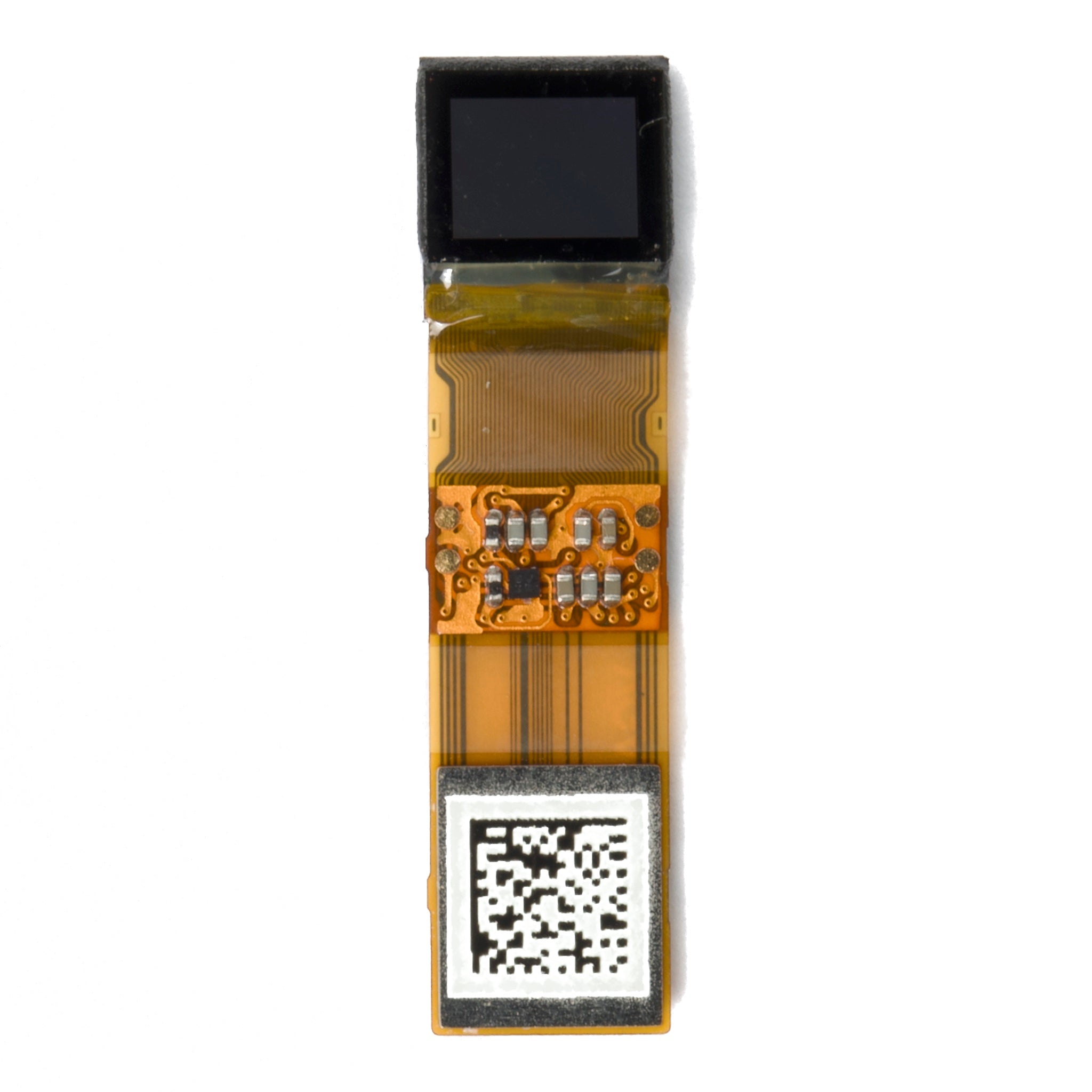
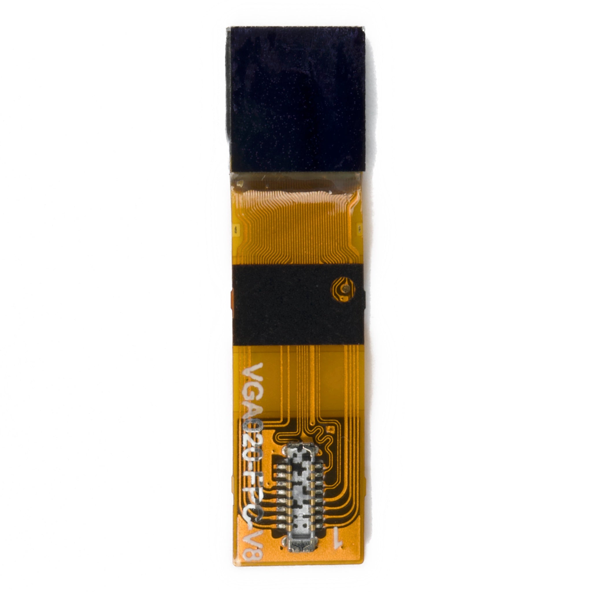
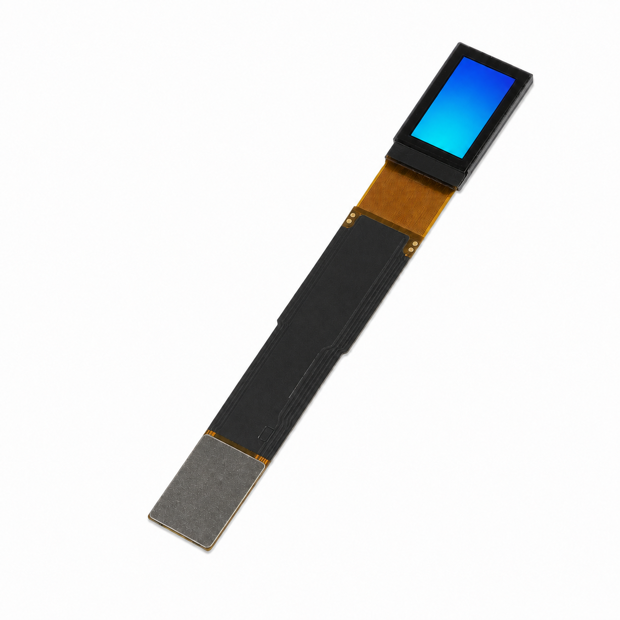
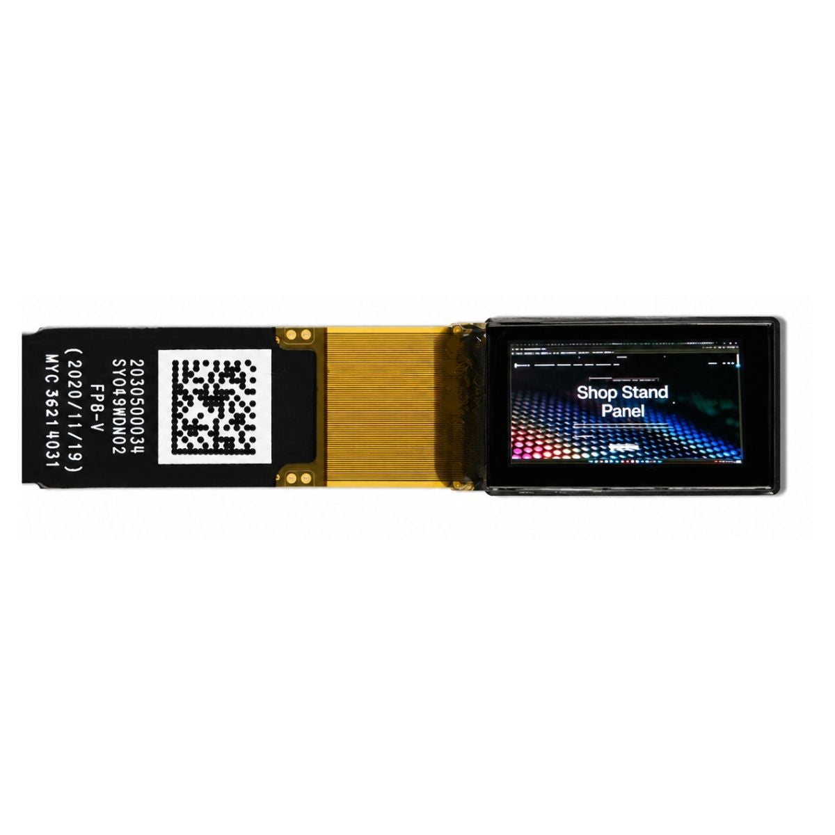
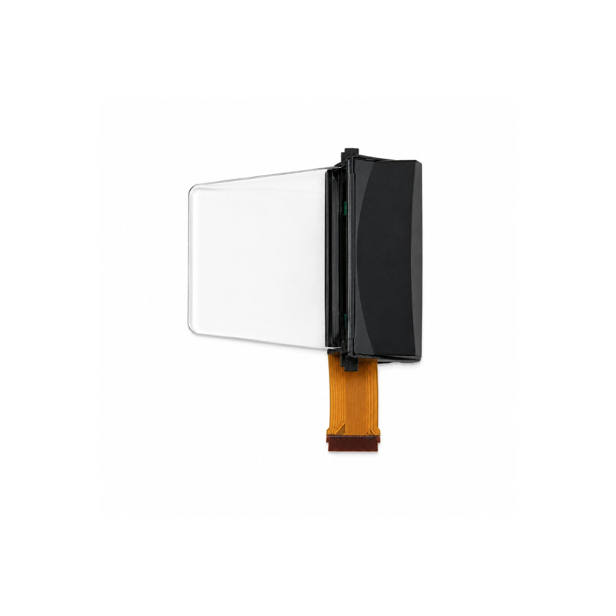
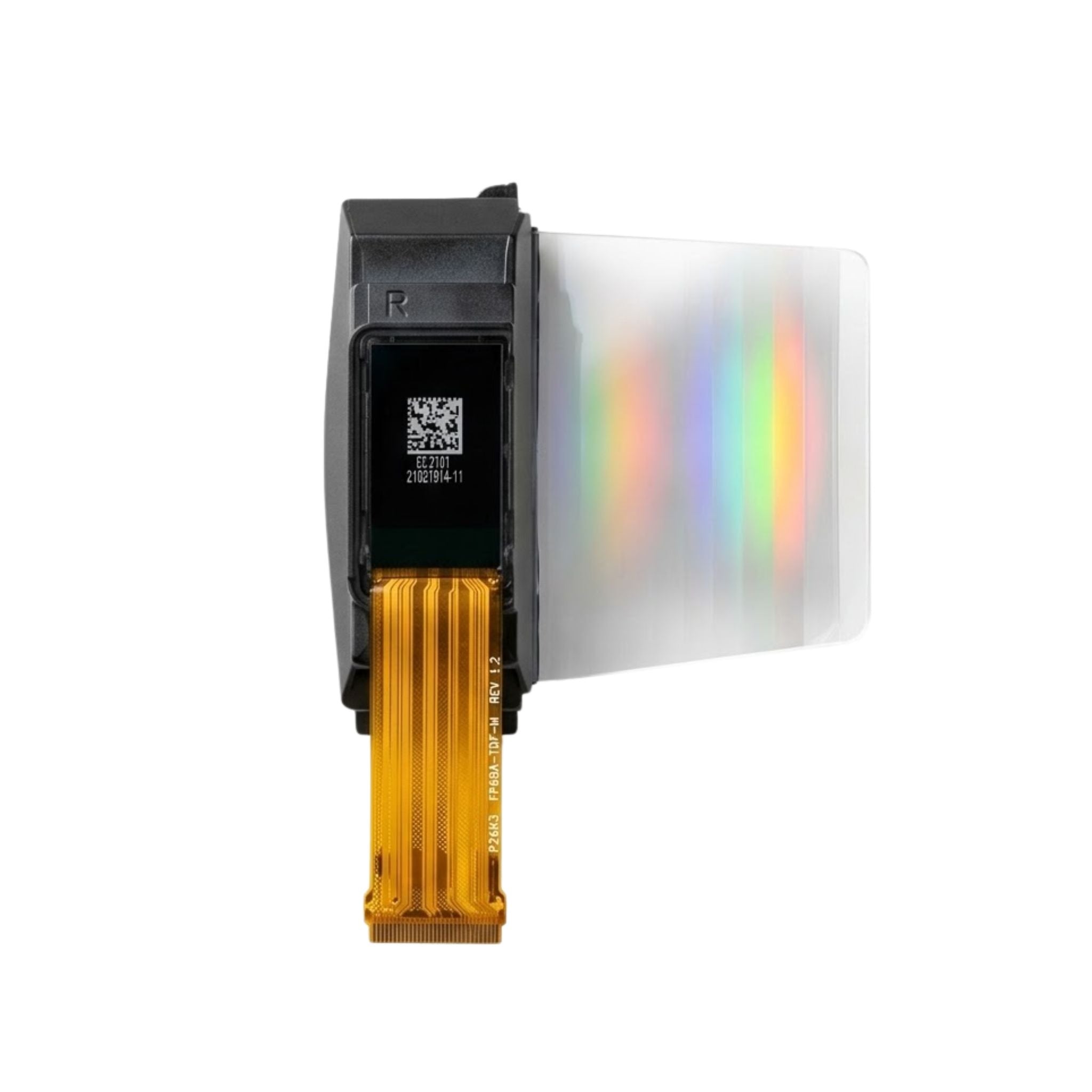
Micro OLED technology is a manufacturing route as much as a display type: organic emitters are deposited on a silicon wafer whose CMOS circuitry drives each pixel, then the wafer is encapsulated, tested and diced into individual panels. Understanding the process explains the cost structure, the yield behaviour and why these panels exist almost exclusively in small, dense formats.[1]
The backplane: where the performance is won
The wafer starts as standard CMOS. Its top metal layer is patterned into pixel electrodes, and the circuitry below provides the drive transistor, the storage capacitor and — depending on the design — some compensation logic. Because the process is a semiconductor process, feature sizes are small and uniformity can be tight, which is what allows pixel pitches of a few micrometres.
The backplane also decides what the panel can do beyond resolution. Current-driving schemes, global dimming and on-panel timing generation are all available because the logic is on the same die. That is why a micro OLED module often needs only a data interface and a supply, with no external row and column drivers.
Depositing the organic layers
Two routes dominate. In the white-plus-colour-filter route, a white emitter stack is deposited across the panel and colour is produced by filters patterned above it. In the separate-emitter route, red, green and blue emitters are deposited in separate regions, typically through fine metal masks.
The filter route is simpler and scales more easily; the emitter route is more efficient because no light is absorbed by filters, but the masks are delicate and limit panel size and resolution. Both routes finish with a cathode and an encapsulation layer, because the organic materials and the cathode react with moisture and oxygen.
Encapsulation decides field life
Thin-film encapsulation is the quiet determinant of reliability. Its job is to keep water vapour and oxygen away from the organic stack for the life of the product, at a permeation rate measured in extremely small units. A panel that passes initial test but has a marginal barrier will develop dark spots spreading from an edge over months.
Because barrier quality is not visible in a datasheet, the practical questions are about process control and about what happens after dicing — where the cut edge is the most vulnerable point. Suppliers who can describe their edge-sealing method are usually the ones who have thought about field returns.
Yield, cost and the dice-per-wafer arithmetic
Yield is measured per wafer, not per display. A defect that ruins one large panel ruins one unit; the same defect on a wafer carrying dozens of micro displays ruins several. That is why micro OLED economics depend on both defect density and panel size: shrinking the panel increases the number of dice per wafer, but each die still needs a working backplane and emitter stack.
Two cost consequences follow for buyers. Test cost matters as much as material cost, because every die must be probed and characterised. And the encapsulation and inspection steps are fixed costs per wafer, which is why very small orders carry a disproportionate premium.
Test, binning and what the numbers mean
Every die is probed before dicing. The tests include pixel-level defects, uniformity, colour coordinates, luminance at a reference current and power at a reference picture level. Panels are then binned by luminance and colour, and the bin determines both price and what optical design can compensate for.
Two consequences follow for buyers. First, the luminance figure in a quotation usually refers to a specific bin; an unusually low price may indicate a lower bin, which the optics will then have to work harder with. Second, colour binning matters for binocular systems, where left and right displays must match closely enough that the fused image does not show a tint difference.
Where the technology is heading
Three directions are visible in the market. Higher luminance, driven by the optical losses of waveguide combiners in AR glasses, where the panel must supply far more light than the eye receives. Larger silicon backplanes, which allow a bigger field of view at the same angular resolution. And tighter integration, with more of the optical and driver function moving onto or beside the die.
For a product designer, the practical reading is that micro OLED specifications should be written in terms of what the optics deliver — luminance at the eye, angular resolution, power at a stated picture level — rather than in terms of panel-only figures.
Cost drivers in the process
Three process steps dominate cost: the backplane wafer, the emitter deposition and the encapsulation. Wafer cost scales with process node and area; emitter deposition cost scales with the number of shadow masks and the deposition time; encapsulation cost scales with the barrier specification and the inspection that verifies it.
That structure explains why a modest resolution increase can move the price sharply — a finer backplane node costs more per wafer, and a higher pixel count per panel reduces the margin for defect density. It also explains why suppliers resist small custom orders: the fixed process costs are spread over too few units.
What to ask a supplier
- Backplane process and pixel pitch, with the resulting panel resolution.
- Colour route and measured gamut, plus the luminance efficiency of each route.
- Encapsulation method and edge-sealing approach.
- Luminance at the eye for the intended optical stack, with the optical assumptions stated.
- Lifetime definition at the operating brightness.
Micro OLED modules are listed in the micro OLED collection; the near-eye systems they serve are covered in the XR display range, and larger emissive panels under AMOLED displays.

Micro OLED manufacturing starts from a CMOS wafer, adds an organic emitter stack and finishes with thin-film encapsulation before dicing. The backplane sets resolution, the encapsulation sets field life, and yield per wafer sets the cost — which is why the technology lives where small panels are used behind magnifying optics.
References
- ISO 9241-307:2008 — Ergonomics of human-system interaction — Part 307: Analysis and compliance test methods for electronic visual displays. International Organization for Standardization. https://www.iso.org/standard/40102.html
더 읽기
Best Micro OLED Modules shine with 2048x2048 pixel resolution for crisp text/images, a 1,000,000:1 contrast ratio deepening blacks/boosting vibrancy, and.
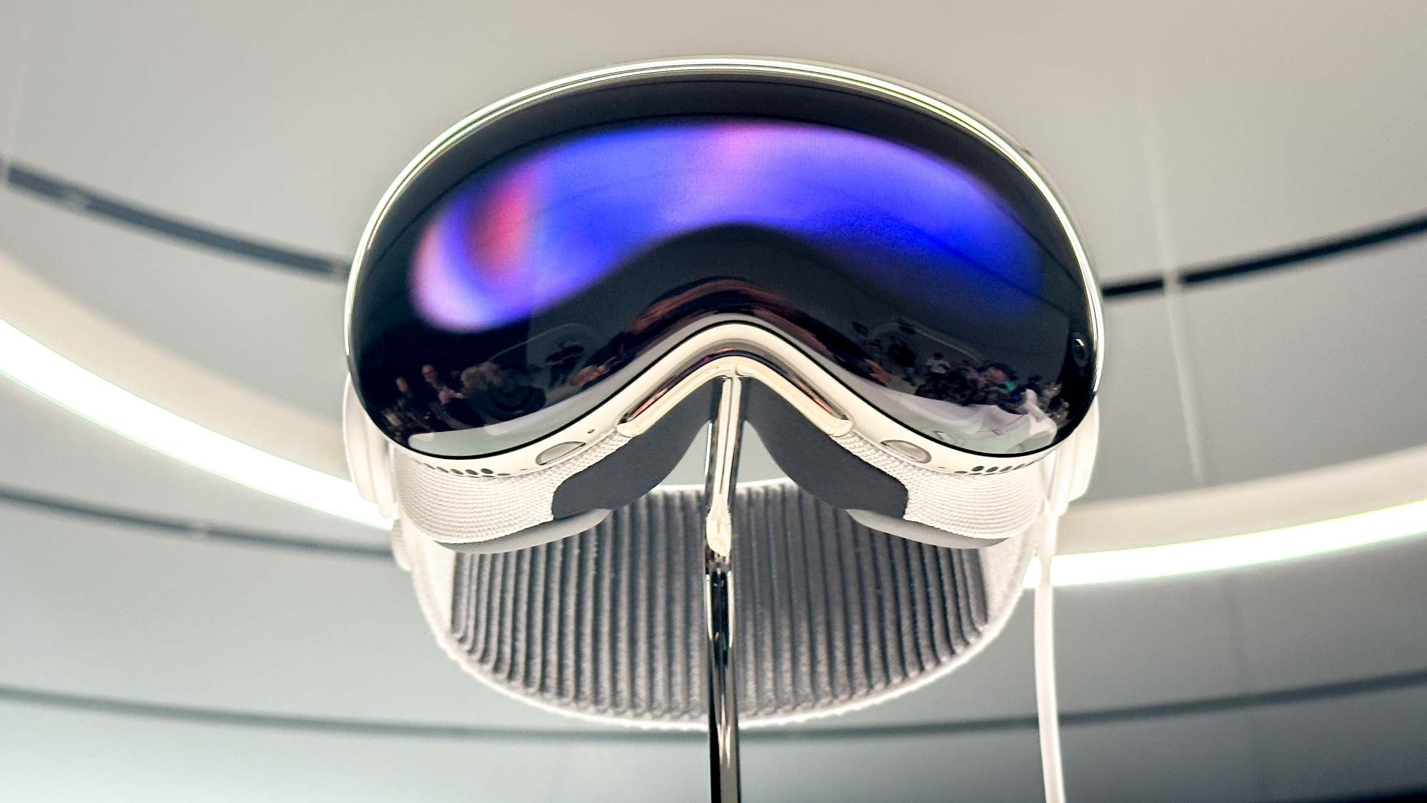
Opt for Micro OLEDs with clear specs: prioritize single/RGB panels (e.g., qVGA 320x240), check response time <0.8ms for motion clarity, and demand.
댓글 남기기
이 사이트는 hCaptcha에 의해 보호되며, hCaptcha의 개인 정보 보호 정책 과 서비스 약관 이 적용됩니다.