


TFT LCD Buying Guide | Resolution, Interface, price
Selecting a TFT LCD requires matching the scenario: MCU or SPI interfaces are suitable for low-resolution screens (such as 240x320), with an average price of about 20 RMB;
High definition requires a MIPI interface paired with 720P or above.
Be sure to verify driver models like ST7789 and pin definitions; prefer LED backlight capacitive screens to ensure durability.
Resolution
On a 7-inch screen, a resolution of 800x480 provides about 133 PPI, suitable for industrial control operation distances of over 60 cm;
If upgraded to 1024x600, data throughput increases by about 60%, usually requiring an upgrade from an RGB interface to LVDS or MIPI to resist interference.
At the same time, high resolution reduces the pixel aperture ratio.
To maintain the same brightness, backlight current usually needs to increase by 20% to 30%, which poses a direct challenge to the battery life of battery-powered equipment.
Visual Density Matching
Calculating Pixel Density
To quantify the fineness of a screen, one cannot look at resolution alone; the PPI (Pixels Per Inch) metric must be introduced.
The calculation logic is simple: first calculate the total number of pixels on the diagonal (using the Pythagorean theorem), then divide by the physical diagonal size (inches) of the screen.
- Formula: PPI = √(Horizontal Pixels^2 + Vertical Pixels^2) / Screen Size
-
Case Analysis:
-
Option A: 10.1 inches, resolution 1280 x 800.
- Diagonal pixels ≈ 1509.
- PPI = 1509 / 10.1 ≈ 149 PPI.
-
Option B: 10.1 inches, resolution 1920 x 1200.
- Diagonal pixels ≈ 2264.
- PPI = 2264 / 10.1 ≈ 224 PPI.
-
Option A: 10.1 inches, resolution 1280 x 800.
How Fine Can the Eye See
Human visual resolution has a physical limit. For an adult with normal vision (20/20 or 1.0), the resolution limit is approximately 1 arcminute, or 1/60th of a degree.
When the angle formed by two pixels in the field of view is less than 1 arcminute, the human eye cannot distinguish them as two dots and will see them as a merged patch.
Based on this physiological limit, we can derive a "Retina Distance" formula:
Ideal Viewing Distance (Inches) ≈ 3438 / PPI
This formula tells us that beyond this distance for a specific PPI, the user will not perceive any graininess.
| Common PPI | Retina Limit Distance | Typical Device | Practical Significance |
|---|---|---|---|
| 326 PPI | ~27 cm (10.5") | Smartphone | Completely grain-free during handheld operation |
| 264 PPI | ~33 cm (13") | High-end Tablet | Very detailed when viewed on a lap or desk |
| 220 PPI | ~40 cm (16") | Laptop | Clear enough under normal typing posture |
| 150 PPI | ~58 cm (23") | Car Center Console/Industrial Control | Golden balance point for driving or standing operation |
| 90 PPI | ~97 cm (38") | Desktop Monitor/Large Screen | No problem at all when viewed from a meter away |
Distance Determines Selection
Based on the above physical laws, when selecting a model for equipment, we should first define the "typical operating distance," then check the table to determine the required PPI, and finally combine with screen size to lock in the resolution.
The Red Line for Handheld Devices (15-30cm)
Handheld terminals (such as medical PDAs, handheld multimeters, smart remote controls) have the closest operating distance. Users may be only 20 cm away from the screen when focusing on reading data.
- Threshold: 250 PPI is the bottom line. Below this value, users will clearly see jagged edges (Aliasing) on fonts, and fine Chinese character strokes will blur together.
-
Recommendation:
- 3.5 inches: Must use 640x960 (326 PPI) or at least 480x800 (266 PPI). If 320x480 (165 PPI) is used, the product will look very retro and cheap.
- 5.0 inches: 720x1280 (HD) is the passing line (294 PPI). 1080x1920 (FHD) is the high-end standard (440 PPI).
Balance at Arm's Length (40-70cm)
This is the most widespread commercial and industrial scenario, including car dashboards, coffee machine interfaces, and CNC machine panels.
- Threshold: 130 - 170 PPI is the most cost-effective range. At this distance, human eye resolution capability declines, and there is no need to pursue smartphone-level detail.
-
Recommendation:
- 7.0 inches: 800x480 (133 PPI) is an industry evergreen; although grainy up close, it is completely acceptable from 50 cm away. If the budget allows, 1024x600 (170 PPI) will make the UI look more refined.
- 10.1 inches: 1280x800 (149 PPI) is the absolute mainstream. The visual improvement from upgrading to 1920x1200 (224 PPI) is not obvious from 60 cm away, but it will significantly increase costs.
Strategy for Far-Field Viewing (>1m)
Elevator advertising machines, airport flight display screens, and factory production line dashboards fall into this category.
- Threshold: < 100 PPI. Here, size (Viewable Area) is more important than resolution. Making the text larger is more critical than making it finer.
-
Recommendation:
- 21.5 inches: 1920x1080 is only 102 PPI, but the effect is excellent when viewed from 1 meter away.
- 32 inches and above: Even with 1366x768 resolution, as long as the brightness is high enough and the contrast is good, it remains an excellent display terminal from 2 meters away.
Side Effects of Pixel Mismatch
If you forcefully display a UI designed for high PPI on a low PPI screen to save trouble, or vice versa, it will cause serious display disasters.
- UI Scaling Blur: Suppose your UI assets are designed for 1920x1080, but you switched to a 1280x720 screen to save money. This non-integer compression (Scaling Ratio ≈ 0.67) will cause line breakage and pixel jitter.
- Anti-aliasing Pressure: Displaying diagonal lines or round buttons on a low PPI (e.g., 130 PPI) industrial screen without a powerful GPU for real-time anti-aliasing will make the "jagged" edges very glaring.
Interface Bandwidth Limitations
Calculate Your Data Traffic
It's not just as simple as Width x Height x Refresh Rate, because after scanning a line and a frame, the screen needs a brief "rest time" to reset signals, known as the Blanking Interval.
Actual data throughput is usually measured by the Pixel Clock (PCLK). The calculation formula is roughly as follows:
PCLK = (Horizontal Resolution + Horizontal Blanking) x (Vertical Resolution + Vertical Blanking) x Refresh Rate
Taking the most common 800x480 resolution, 60Hz refresh rate as an example:
- Horizontal Total (HT): 800 (Display) + 256 (Blanking) = 1056 clocks
- Vertical Total (VT): 480 (Display) + 45 (Blanking) = 525 lines
- PCLK: 1056 x 525 x 60 ≈ 33.2 MHz
If it is RGB888 format (24 bits per pixel), the total data bandwidth is 33.2 MHz x 24 bit ≈ 796 Mbps.
Slow Serial Interfaces Are Only Suitable for Static Images
SPI and I2C are the most common low-speed interfaces, typically having only 1 to 4 data lines.
- Bandwidth Cap: Standard SPI interface clock frequency is usually limited to under 50MHz.
- Actual Experience: Driving a small 320x240 screen (QVGA) with 16-bit color per pixel (RGB565). The data volume for one frame is 320 x 240 x 16 = 1,228,800 bits.
- Refresh Rate Trap: Under a 50MHz SPI clock, the theoretical fastest transmission for one frame takes about 0.024 seconds, or roughly 40fps maximum. But this is just a theoretical value; adding instruction overhead and MCU processing delay, the actual rate is often only 20-30fps.
If you attempt to drive 480x320 or higher resolution with SPI, you will visibly see the screen refreshing line by line like blinds; this is the "tearing" sensation caused by insufficient bandwidth.
Signal Interference in Parallel Interfaces
To solve the speed problem, engineers devised the "multi-lane parallel" method, which is the RGB and MCU (8080/6800) interface.
The RGB888 interface transmits 24 bits of data at once, equivalent to 24 lanes running simultaneously.
- Physical Limit: The biggest enemies of parallel interfaces are Signal Skew and Electromagnetic Interference (EMI). When 24 data lines flip levels simultaneously at frequencies above 30MHz, huge crosstalk is generated between them.
- Distance Limit: This is why RGB interface cables (FPC) usually cannot exceed 15-20 centimeters.
- Frequency Ceiling: For RGB interfaces with TTL levels (3.3V), it is difficult for PCLK to exceed 50-60 MHz. 800x480 is its comfort zone; it can barely handle 1024x600, but going higher (like 1280x800), parallel signal integrity is hard to guarantee.
Differential Signals Solve High-Speed Transmission
When resolution reaches High Definition (HD, 1280x720) levels, PCLK typically exceeds 70 MHz, and traditional parallel interfaces fail completely.
LVDS no longer uses high voltage swings of 3.3V, but instead uses the voltage difference between a pair of wires (about 350mV) to represent 0 and 1.
- Anti-interference Ability: Because transmission is paired, external noise acts on both lines simultaneously and cancels out. This allows LVDS to run very fast, and cables can be made longer (up to 50-100 cm).
-
Channel Quantity:
- Single-channel LVDS (1-ch): Usually consists of 4 pairs of data lines + 1 pair of clock lines, supporting up to roughly 1366x768 @ 60Hz.
- Dual-channel LVDS (2-ch): Uses 8 pairs of data lines + 2 pairs of clock lines, doubling bandwidth; it is standard for 1920x1080 (FHD) panels.
MIPI Channels Dedicated to Phone Screens
Modern phone screens easily hit 2K resolution, and LVDS bandwidth is stretched thin; moreover, LVDS power consumption is high for battery devices. MIPI-DSI (Mobile Industry Processor Interface) was born for this.
- Speed and Power: MIPI DSI uses more advanced signal transmission protocols; the speed of a single data channel (Lane) can reach 1Gbps or even 2.5Gbps.
-
Flexible Configuration:
- 2-Lane: Usually used for screens from 480x800 to 720x1280.
- 4-Lane: Standard HD configuration, easily supporting 1920x1080 @ 60Hz or even higher.
- Video Memory Mode: MIPI screens are usually divided into Video Mode (the main controller sends data non-stop) and Command Mode. MIPI screens with RAM can let the main controller sleep when the image is static, greatly saving bandwidth and power, which is the secret to long battery life in smartwatches.
Brightness and Power Balance
The Denser the Pixels, the Thicker the Window Frame
Imagine every pixel as a window. Low-resolution screens are like large floor-to-ceiling windows; the glass area is large, the frame is thin, and sunlight enters easily.
Although pixels become smaller, the Thin Film Transistors (TFT) controlling each pixel switch, the capacitors storing charge, and the metal traces transmitting signals (Gate Lines and Source Lines) are difficult to shrink proportionally.
It's like replacing a large floor-to-ceiling window with dense security bars; the frames and bars occupy most of the area, and the actual glass area that lets light through becomes smaller.
-
Aperture Ratio: This refers to the proportion of effective light-transmitting area to total pixel area.
- Low-Res Screen (e.g., 800x480): Pixels are larger, transistor blocking is minimal, and aperture ratio can usually reach 60% or higher.
- High-Res Screen (e.g., 1920x1080): Pixels are extremely dense, Black Matrix and wiring blockage is severe, and aperture ratio often drops to 40% or even 30%.
Same Brightness Requires Double the Power
After light is emitted from the backlight LED, it must pass five hurdles to reach the human eye:
- Rear Polarizer: Filters out 50% of the light.
- Glass Substrate and TFT: Depending on the aperture ratio, another 40% - 60% of light is lost.
- Color Filter (CF): To display RGB colors, each sub-pixel only allows Red, Green, or Blue to pass, chopping off about 70% of the light.
- Front Polarizer: A bit more loss.
If you choose a high-resolution screen (low aperture ratio), light transmittance might drop below 4%.
To allow users to see the screen clearly outdoors (e.g., needing 800 nits), you must frantically increase the brightness of the backlight LED.
Data Comparison:
Assume a 7-inch screen requiring a surface brightness of 1000 nits:
- 800x480 Resolution: High aperture ratio, backlight might only need to provide 12,000 nits of initial brightness. Power consumption might be around 2.5W.
- 1920x1200 Resolution: Low aperture ratio, backlight must provide close to 20,000 nits of initial brightness to penetrate that dense grid. Power consumption might soar to 4.5W or higher.
This extra 2W of power consumption directly shortens the battery life of a 5000mAh (3.7V, 18.5Wh) battery by several hours.
Changing Material Might Save Some Power
Since a-Si (Amorphous Silicon) technology transistors can't be made small and block too much light, panel manufacturers developed advanced materials to increase Electron Mobility, allowing transistors to be made very small to save power at high resolutions.
- a-Si (Amorphous Silicon): Electrons run slowly, so transistors must be made large to pass enough current. This leads to extremely low aperture ratios at high PPI, consuming the most power. Typically used for screens under 300 PPI.
- LTPS (Low-Temperature Polycrystalline Silicon): Electron mobility is over 100 times that of a-Si. Transistors can be made very tiny, and lines can be thinner. This allows high-resolution screens to have decent aperture ratios. Although LTPS panels are expensive, their backlight power consumption can be 30% - 40% lower than a-Si for the same brightness.
- IGZO (Indium Gallium Zinc Oxide): In between the two, with extremely low leakage current, suitable for scenarios requiring power saving on static images, and transmittance better than a-Si.
Electrical Energy Eventually Becomes a Hot Potato
The side effect of increasing backlight power is not just fast battery drain, but also heat.
As current density increases, LEDs suffer from Droop Effect, meaning the higher the current, the higher the proportion of heat generation, and the proportion converted to light decreases.
When you forcefully increase current to compensate for the low transmittance of a high-res screen, a large amount of energy is converted into waste heat.
- LED Aging: Long-term high-temperature operation accelerates the decay of LED phosphors, causing the screen to turn yellow or dim after a year.
- Liquid Crystal Blackening: TFT LCD liquid crystal materials are sensitive to temperature. If the backlight strip generates too much heat and heat dissipation design is poor, the bottom of the screen may reach 60°C - 80°C.
Interface
Low-speed SPI interfaces require only 3 to 4 signal lines to drive small screens of 320x240 resolution, but video frame rates are low due to clock frequency limitations around 50MHz.
The MCU 8080 parallel bus improves transmission efficiency through 8-bit, 16-bit, or 18-bit data width, and its built-in video memory (GRAM) feature makes it suitable for static displays of 480x320 specifications.
For high-definition screens above 1024x600, RGB TTL requires occupying 40+ GPIO pins to maintain a 60Hz refresh rate, while MIPI DSI utilizes low-voltage differential signals to provide 1Gbps+ rates over 4 channels (Lanes), being the standard for 1080p mobile devices.
Industrial-grade large screens over 10 inches often use LVDS, utilizing differential signal anti-interference characteristics to achieve long-distance transmission of over 5 meters.
SPI Serial Transmission
How Four Wires Move
Standard SPI TFT screens are usually called 4-line SPI. These four wires are Chip Select (CS), Clock (SCLK), Data Input (MOSI/SDA), and Data/Command Switch (DC/RS).
- Clock Frequency Data: The maximum SPI clock frequency supported by most TFT driver ICs (such as ST7789V or ILI9341) is between 10MHz and 50MHz. At a 50MHz clock, the theoretical maximum transfer rate is 6.25MB per second.
- Sync Logic: SCLK is generated by the main control board to ensure data bits are accurately sampled on the rising or falling edge.
- Bidirectional Communication Limit: Although the SPI protocol supports full duplex (MISO line), in TFT screen applications, since the screen side usually does not return large amounts of data, MISO is often omitted to save pins, or used only for reading register status.
Bandwidth Calculation Process
The following is a calculation based on 240x320 resolution and 16-bit (RGB565) color mode.
- Single Frame Data Volume: 240 times 320 times 2 bytes (16 bits), totaling 153,600 bytes.
- Transmission Time: If the clock runs at 20MHz (approx. 2.5MB/s), transmitting one frame of image takes about 0.06 seconds.
- Refresh Rate Cap: Under this configuration, the theoretical frame rate can only reach 16fps at most. If smooth 60fps animation is needed, the SPI physical layer bandwidth gap is as high as 4 times.
- Optimization Means: Developers typically use "partial refresh" technology, updating only the pixel areas on the screen that have changed, thereby achieving smooth digital jumping effects on a low-speed bus.
Data Line Variants
To squeeze more performance out of limited pins, the industry has derived several non-standard SPI variants.
- 3-line SPI: Eliminates the hardware DC pin. It adds 1 bit before sending every 8 bits of data to identify whether it is a command or a pixel. This mode changes the packet length to 9 bits; although it saves a wire, many microcontroller hardware SPI controllers do not support non-8-bit alignment, forcing the use of simulated IO (bit-banging), which actually lowers efficiency.
- Dual SPI / Quad SPI: This is a high-performance solution from recent years. By adding 1 or 3 data lines, 2 or 4 bits of data are transmitted within the same clock cycle. Under a 50MHz clock, Quad SPI throughput can increase to 25MB/s, enough to support smooth interaction at 320x480 sizes.
Signal Quality Control
Although SPI is simple, physical circuit electrical characteristics directly affect display quality when running at high frequencies (>20MHz).
- Impedance Matching: Long-distance transmission causes signal reflection. Resistors of 22 to 47 ohms are usually connected in series on the clock and data lines at the master end to suppress overshoot.
- Trace Length: SPI is a single-ended signal and lacks anti-interference ability. If the FPC cable or PCB trace exceeds 15 cm, the clock signal will distort, causing display artifacts or a white screen.
- Level Shifting: Most TFT driver ICs work at 1.8V or 3.3V logic levels. If the main control board outputs 5V levels, high-speed level shifting chips must be used; simple resistor voltage dividers will cause severe waveform deformation and cannot support high-speed clocks.
Hardware and Software Overhead
The SPI interface has a dual nature regarding resource occupation on the main control board.
- GPIO Resources: Extremely friendly to IO resources. A master supporting 4 SPI channels can control 4 screens simultaneously, whereas an RGB interface can typically only drive 1 screen.
- CPU Usage: This is SPI's weakness. Since data must be moved by the CPU or DMA, high system load is generated during screen refreshing.
- Role of DMA: In high-performance embedded designs, DMA (Direct Memory Access) technology must be used. The CPU only needs to issue a "start transfer" command, and the DMA controller will push data from the Frame Buffer to the SPI bus in the background. This can reduce CPU usage from over 90% to around 5%.
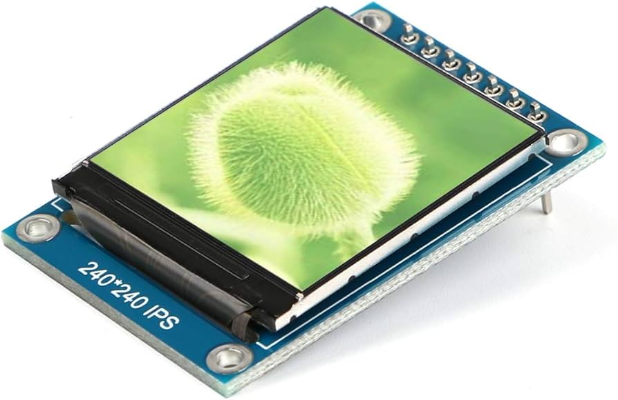
Common Driver Chips
| Chip Model | Supported Resolution | Features |
|---|---|---|
| ST7735 | 128x160 | Extremely low cost, widely compatible, common in 1.8-inch screens |
| ILI9341 | 240x320 | Classic 2.4/2.8-inch screen driver, supports parallel/serial switching |
| GC9A01 | 240x240 | Dedicated for circular screens, widely used in smartwatches |
| ST7789V | 240x320 | No external crystal needed, high integration, supports high-speed SPI |
Selection Judgment Basis
Before deciding to use an SPI interface, please check if your project meets the following quantitative standards:
- High Proportion of Static Display: If the interface is mainly text, icons, or slowly changing curves, SPI is the best cost-effective choice.
- Limited Master Performance: If the RAM of the master chip (like a microcontroller) is less than 256KB and cannot establish a complete RGB frame buffer, you must choose an SPI screen with GRAM.
- Extremely Limited Space: In wearable devices, every 1mm increase in FPC cable width affects stacking; SPI's 4-10 pin connector advantage is huge.
MCU Parallel Bus
How to Connect a Bunch of Wires
To drive a screen with an MCU interface, you need to reserve a large number of GPIO pins on the main control board.
-
Data Bus (DB0-DBx): This is the channel for transmitting pixel data.
- 8-bit Mode: Saves the most pins, but transmitting a 16-bit color pixel requires writing data twice (high 8 bits first, then low 8 bits).
- 16-bit Mode: Current mainstream configuration. A complete RGB565 pixel can be transmitted in one write cycle, doubling efficiency compared to 8-bit.
- 18-bit / 24-bit Mode: Used for pursuing ultimate color (RGB666 or RGB888), but rare in embedded applications because it occupies an extra 2 to 8 GPIOs.
-
Control Signal Lines:
- CS (Chip Select): Chip select signal; the screen obeys commands only when pulled low.
- RS (Register Select) / DC (Data/Command): This is the switch distinguishing "data" from "instruction." High level means sending pixel color; low level means sending setting instructions (like setting window position).
- WR (Write): Write signal. On the rising edge, the screen latches data on the bus.
- RD (Read): Read signal. Used to read screen ID or video memory content. Many unidirectional display applications connect this pin directly to high level to save an IO.
- RESET: Hardware reset pin.
How Fast Can It Actually Run
Checking data sheets of common driver ICs (like ILI9488), the minimum write cycle is usually between 66ns and 100ns.
Assume using a 16-bit parallel bus to drive a 480x320 resolution screen.
- Single Frame Pixel Count: 153,600 pixels.
- Data Throughput: Since it is 16-bit parallel, each pixel only requires 1 write operation.
- Theoretical Time: If the master IO toggling speed is fast enough to reach 10MHz (100ns cycle), filling a full frame of data takes about 15.3 milliseconds.
- Frame Rate Cap: Theoretically can reach 65fps.
But if resolution increases to 800x480 (384,000 pixels), at the same 10MHz write speed, one frame takes 38.4 milliseconds, and the frame rate instantly drops to 26fps.
This is why MCU interfaces are generally not recommended for high-definition screens above 800x480, unless your master can achieve extremely high bus speeds.
The Screen Remembers Things Itself
The biggest difference between MCU interfaces and RGB interfaces is that MCU screens come with GRAM (Graphic RAM).
- Zero Burden for Static Images: After you write an image to the screen, the master chip can completely stop sending data or even enter sleep mode, and the screen will stably display the image just sent.
- The Art of Partial Refresh: You don't need to redraw the entire screen every time. By sending "Column Address Set" and "Page Address Set" instructions, you can define a rectangular window (Window Address) on the screen and then write data only to this window. For example, updating only the battery icon in the upper right corner might involve data volume only 1% of the full screen, completed instantly.
The Grudge Between 8080 and 6800
When purchasing or configuring, you will often see "8080 Timing" and "6800 Timing" options. They originate from early Intel 8080 processors and Motorola 6800 processors.
- Intel 8080 Mode: Uses independent WR (Write) and RD (Read) pins. This is the most common default configuration in current TFT modules.
- Motorola 6800 Mode: Uses E (Enable) pin and R/W (Read/Write direction) pin.
- Compatibility: Modern driver ICs usually support both modes simultaneously, switching hardware via the logic levels of IM0/IM1/IM2 pins on the FPC cable.
That One Wire Against Tearing
When playing animations or videos, MCU interfaces are prone to "Screen Tearing" phenomena.
To solve this, TFT modules usually bring out a TE (Tearing Effect) pin.
- Working Principle: The screen controller periodically outputs a pulse signal telling the master: "I have just finished scanning a frame and am in the vertical blanking period (V-Blanking); you can start writing new data."
- Synchronization Mechanism: After detecting the TE signal, the master immediately starts DMA data transfer, ensuring orderly writing into video memory before the screen starts the next frame scan or during the scan, thereby achieving silky smooth animation effects.
RGB Direct Connection Mode
Brainless Screen Modules
In RGB mode, the LCD driver IC (like EK79001 or HX8264) is in a "dummy mode."
It is not responsible for remembering any image data; it only takes charge of projecting received electrical signals onto corresponding liquid crystal units.
- Workflow: The master CPU sends the color value of each pixel sequentially from left to right, top to bottom, through data lines.
- Refresh Pressure: To deceive the human eye into creating the illusion of a continuous picture, the master must repeat this process 60 times per second (60Hz).
-
Signal Composition: Besides RGB data lines, four rigid sync signals are needed:
- VSYNC (Vertical Sync): Tells the screen "A new frame has started."
- HSYNC (Horizontal Sync): Tells the screen "This line is finished, switch to the next line."
- DE (Data Enable): Tells the screen "The data on the line now is valid pixel data, not black borders."
- PCLK (Pixel Clock): Metronome. With every clock pulse, the screen reads one pixel dot.
Arithmetic of Memory and Bandwidth
Before using an RGB interface, the master chip's resource bill must be calculated. Since the screen has no video memory, the master chip must allocate a frame buffer in its own RAM.
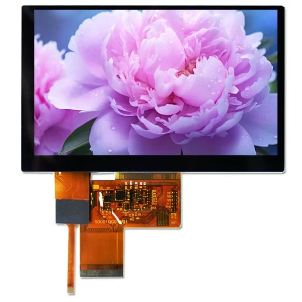
Taking a common 800x480 resolution, RGB565 (16-bit) format 7-inch screen as an example:
-
Video Memory Usage: 800 times 480 times 2 bytes = 768 KB.
- Most mid-range microcontrollers (like STM32F407) with only 256KB or 512KB of internal RAM simply cannot establish a full-screen buffer.
- Solution: Must mount an external SDRAM chip, or choose high-end models (like H7 series) with several megabytes of internal RAM.
-
Bus Bandwidth:
- Pixel Clock (PCLK) needs about 30 MHz to 33 MHz.
- Data Throughput: 30M times 2 bytes = 60 MB/s.
- The master's memory bus needs to move 60MB of data to the screen per second. If your program is reading/writing an SD card or running complex algorithms simultaneously, the bus might get congested, causing screen ripples or tearing.
Timetables That Must Align
The most time-consuming part of RGB interface debugging is gathering "Timing Parameters." The screen does not start displaying the moment it receives a signal; like old CRT TVs, it needs "retrace" time.
You need to precisely fill in the following parameters in the software driver (units are usually PCLK clock cycles):
| Parameter Name | Abbreviation | Typical Value (800x480) | Function |
|---|---|---|---|
| Pulse Width | HPW/VPW | 1 - 48 | Length of time the sync signal remains valid |
| Back Porch | HBP/VBP | 40 - 88 | How long to wait after sync signal ends before sending data (Left/Top black border) |
| Front Porch | HFP/VFP | 10 - 200 | How long to rest after sending one line/frame of data before sending the next sync signal (Right/Bottom black border) |
-
Symptom Diagnosis:
- If the image shifts right overall: HBP (Horizontal Back Porch) setting is too large.
- If there is noise or jitter at the screen edge: Porch parameters do not match the screen factory datasheet.
- DE Mode: Many modern RGB screens support "DE Mode." In this mode, you don't need to worry about specific pulse widths of HSYNC and VSYNC; as long as the DE signal is pulled high, the screen considers it valid data.
Physical Connection of Color Channels
RGB interfaces are divided into different levels based on the number of data lines, which determines color smoothness.
-
RGB565 (16-bit): 5 bits Red, 6 bits Green, 5 bits Blue.
- Pin Count: 16 data lines.
- Effect: 65,000 colors. Slight ripples (color banding) are visible to the naked eye when displaying blue skies or gradients.
- Usage: Industrial control, meters with low color requirements.
-
RGB666 (18-bit): 6 bits each for Red, Green, Blue.
- Pin Count: 18 data lines.
- Effect: 260,000 colors. Finer than 565, but awkward because most masters are 16-bit or 32-bit architectures, making 18-bit data handling cumbersome.
-
RGB888 (24-bit): 8 bits each for Red, Green, Blue.
- Pin Count: 24 data lines.
- Effect: 16.7 million colors (True Color). Gradients are perfectly smooth.
- Wiring Tip: If the master only has an RGB565 interface but the screen is RGB888, you should connect the master's R0-R4 to the screen's R3-R7 (high bit alignment) and ground the screen's remaining low bits (R0-R2).
Can Only Be Short, Not Long
RGB interfaces use TTL level signals (usually 3.3V). This signal has extremely weak anti-interference capabilities at high frequencies of 33MHz or even 50MHz.
- EMI Radiation: When 24 data lines flip levels simultaneously, they emit electromagnetic waves outward like 24 small antennas. This not only makes it hard for the product to pass CE/FCC certification but may also interfere with onboard GPS or WiFi modules.
-
Transmission Distance:
- Safe Distance: FPC cable length is best controlled within 10cm - 15cm.
- Consequences of Being Too Long: Once exceeding 20cm, signals will experience crosstalk. You will see the screen image turning white, appearance of snow noise, or color jitter.
- Solution: If long-distance transmission is mandatory, do not force the use of RGB wires; add an RGB to LVDS or RGB to HDMI chip.
Rules of the 40Pin World
In the general-purpose LCD market for 4.3-inch, 5.0-inch, and 7.0-inch screens, there exists a de facto standard interface definition, commonly referred to as "Universal 40Pin RGB."
- Pin Pitch: 0.5mm.
- Backlight Power: Usually integrated within the cable (LED+ and LED-).
-
Touch Screen:
- If it is a Resistive Screen, the 40Pin interface usually includes X1/X2/Y1/Y2 four resistive touch lines.
- If it is a Capacitive Screen, usually the capacitive screen will have its own independent 6Pin I2C interface cable and does not go through this large 40Pin channel.
Price
The quotation for a TFT LCD module consists of three major parts: Open Cell (LCD Panel), Driver IC, and Backlight Module.
Among them, the panel typically accounts for 50% to 60% of the total BOM cost.
If custom requirements are added, such as high brightness backlight over 1000 nits or Capacitive Touch Screen (PCAP) optical bonding, it usually incurs an NRE (Non-Recurring Engineering fee) ranging from $500 to $5,000.
Furthermore, interface selection (e.g., MIPI vs RGB) changes the Driver IC selection, resulting in a unit price difference of $0.5 to $2.0.
Procurement scale has a significant impact on unit price; transitioning from the sample stage to 10k-level mass production typically lowers the unit price by 15% to 30% due to the amortization of fixed manufacturing costs.
Hardware Costs
LCD Panel Glass
The LCD panel (Open Cell) usually occupies 50% to 60% of the total cost; it is the most significant part determining display effect and price baseline.
-
Glass Substrate Utilization
Panel factories categorize by "Generation Line," such as Gen 6 or Gen 8.5 lines. The number of screens that can be cut from a huge mother glass directly determines the single-piece cost. If your size efficiency on a certain generation line is only 85%, while another standard size reaches 95%, the former's unit price will be about 10% higher due to waste amortization. -
Glass Thickness and Thinning Process
Standard glass thickness is usually 0.5mm or 0.4mm. If the application scenario requires extreme thinness, secondary chemical thinning (Slimming) of the glass is needed, adding a process step and breakage risk, causing panel cost to rise by about $1.0 - $2.0. -
Liquid Crystal Material Grade
Liquid crystal molecule response speed and temperature stability are graded. Liquid crystal materials used for -30°C low-temperature environments must have special anti-viscosity components added to their formula, priced at 1.2 times that of ordinary 0°C commercial-grade liquid crystal.
Driver Chip IC
Although small in volume, its cost share is usually 10% - 15%.
-
Wafer Foundry Capacity
LCD driver chips are mainly manufactured using 8-inch wafer processes. This is a mature process with extremely tight capacity globally. When demand for Power Management ICs (PMIC) or automotive electronics squeezes 8-inch wafer capacity, driver IC lead times lengthen, and spot prices may fluctuate by over $0.50 within weeks. -
Packaging Form (COG vs COF)
- COG (Chip on Glass): Chip bonded directly on glass. Lowest cost, but requires glass to leave a wider bottom border for routing, affecting screen-to-body ratio.
- COF (Chip on Film): Chip bonded on a flexible circuit board, which can be folded to the back of the screen. This process achieves extremely narrow bezels, but the cost of a single FPC is $1.5 - $3.0 higher than the COG solution, and assembly precision requirements are extremely high.
-
Built-in Memory (RAM)
A driver IC integrated with 1MB GRAM (for 320x480 resolution) is about $0.80 more expensive than a pure RGB interface driver IC without RAM.
Backlight Module Components
The Backlight (Backlight Unit, BLU) is not just a few LED lights; it is a precision optical system, accounting for about 20% of cost, with high elasticity based on brightness needs.
-
Light Guide Plate Material (LGP)
- PMMA (Acrylic): Extremely high transmittance (92%+), not prone to yellowing, first choice for high-quality modules, but price is higher.
- PS (Polystyrene): Cheap, but prone to yellowing under long-term heat, causing screen color temperature drift. Using PS material can lower backlight cost by 15%, but sacrifices long-term reliability.
-
Optical Film Stack
Standard backlight structure usually contains "1 Diffusion Film + 2 Brightness Enhancement Films (Prism Sheet)."- If brightness needs boosting, a DBEF (Dual Brightness Enhancement Film) can be added. This is a high-end film dominated by 3M, capable of recycling polarized light to boost brightness by 30%, but the cost per sheet can be as high as $0.50 - $1.00, potentially exceeding the total cost of LED beads.
-
LED Heat Dissipation Bracket
For high brightness screens over 1000 nits, ordinary FR4 material light strips cannot satisfy heat dissipation and must be replaced with Aluminum PCB, doubling the light strip cost.
Polarizer
Polarizers are pasted on the top and bottom sides of the glass substrate, determining the screen's viewing angle and anti-reflection capability.
-
Wide Temperature and Durability
Ordinary polarizers may bubble or peel after 500 hours of testing in high temperature and high humidity (e.g., 60°C / 90% RH) environments. Industrial-grade polarizers use special iodine or dye-based formulas capable of withstanding 85°C high temperatures, priced 20% - 30% higher than consumer-grade polarizers. -
Surface Treatment
- Anti-Glare (AG): Reduces reflection through surface atomization treatment, suitable for outdoor or strong light environments, requiring an additional process cost of about $0.30.
- Anti-Reflection (AR): Eliminates reflected light through multi-layer coating technology, best effect but extremely expensive, usually only used for military or aviation-grade displays.
Flexible Printed Circuit
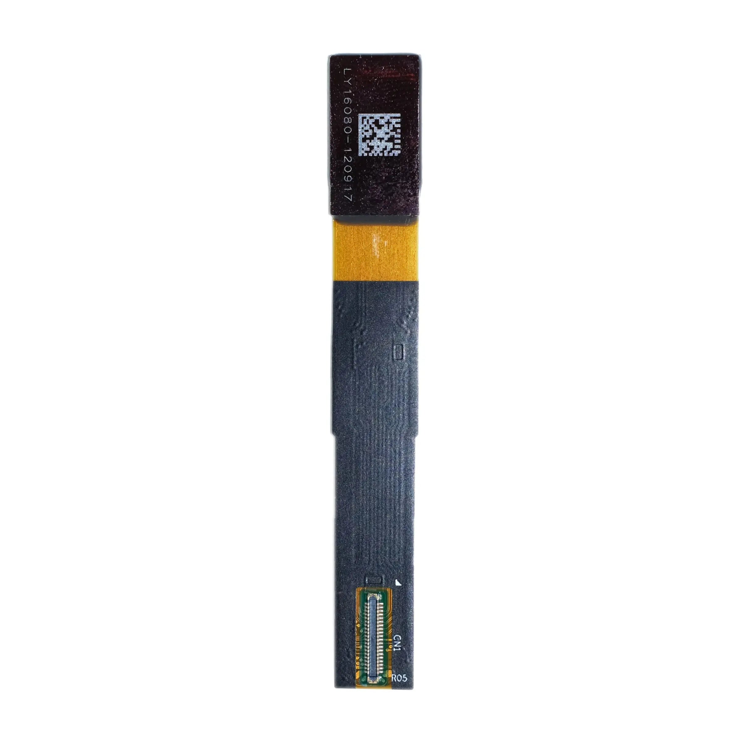
FPC (Flexible Printed Circuit) connects the screen to the motherboard. Its process details are often overlooked but are sources of hidden costs.
| Parameter | Low Cost Solution | High Reliability Solution | Estimated Cost Difference |
|---|---|---|---|
| Layers | Single or Double layer board | 4-layer board (with independent ground layer) | + $0.40 |
| EMI Shielding | Silver paste printing | EMI Shielding Film | + $0.20 |
| Surface Treatment | Tin plating (OSP) | Immersion Gold (ENIG, >2u") | + $0.15 |
-
Immersion Gold Process
In the gold finger (Pin) part of the FPC, low-cost screens may use tin plating, which easily oxidizes and causes poor contact after multiple insertions. High-spec screens require Immersion Gold process; the thicker the gold layer, the better the oxidation resistance, but this directly consumes precious metal costs.
Assembly Consumables
-
ACF (Anisotropic Conductive Film)
Conductive tape used to bond FPC or IC to glass. Japanese brands (like Sony, Hitachi) have uniform conductive particles and high yields, but the price is 2 times that of domestic glue. Although this only accounts for a few cents in a single BOM, in mass production, it affects First Pass Yield; rework costs caused by low-quality glue are far higher than the price difference of the glue itself. -
Iron Frame and Bezel
- SUS (Stainless Steel): High strength, not prone to rust, exquisite appearance.
-
SGCC (Galvanized Steel Sheet): Low cost, prone to rust at cut edges.
Choosing SUS304 stainless steel bezel costs about $0.20 more than ordinary galvanized iron frame, but significantly improves the module's structural strength and corrosion resistance.
Spec Impact on Price
The Game Between Pixel Density and Yield
The cost increase brought by resolution improvement is not just about cutting a few more pixels. Behind it lies the direct challenge of manufacturing yield rate.
-
Precision Cost of Mask Process
Making 800x480 resolution on a 5-inch screen involves large pixels and low requirements for lithography machine precision. But if the same size is to be 1920x1080 (FHD), pixel density (PPI) surges. This requires TFT array etching precision to reach the micron level. Once a transistor (TFT) of a sub-pixel shorts or breaks, the entire screen becomes a defect. For high PPI screens, factories must use more expensive exposure machines, and the production line yield may drop from 98% to 92%. The cost of this lost 6% capacity will be directly amortized into every good unit shipped, causing the unit price to float up by 15% - 20%. -
Backlight Surcharge Caused by Lower Aperture Ratio
The higher the pixels, the denser the wiring, and the larger the proportion of light-blocking Black Matrix and transistor areas, the lower the "Aperture Ratio" for light transmission. To maintain the same surface brightness (e.g., 400 nits), high-res screens must use stronger backlight modules. You not only pay for expensive panels but also spend an extra $0.5 - $1.0 to upgrade LED bead quantity or brightness enhancement films to compensate for light blocked by high-density pixels.
Generational Gap in Panel Technology
The price difference between IPS and TN stems from differences in underlying physical structure, which directly determines time costs on the production line.
-
Mask Steps
Manufacturing a TN panel usually requires 4 to 5 mask processes in standard procedure. However, manufacturing a high-quality IPS or FFS panel requires more complex electrode structures to control planar rotation of liquid crystal molecules, typically requiring 5 to 7 mask processes. Each mask process includes a complete flow of cleaning, film formation, photoresist coating, exposure, developing, etching, and stripping. Two extra processes increase the dwell time (Tact Time) of each glass sheet on the production line by 30%, and consumption of equipment depreciation, water, electricity, and gas increases accordingly. -
Liquid Crystal Material
IPS-specific liquid crystals have special dielectric anisotropy, and their chemical synthesis difficulty is higher than ordinary TN liquid crystals. For top-tier manufacturers (like Merck), the selling price of IPS liquid crystal mixtures is usually 40% higher than TN liquid crystals. Although liquid crystal accounts for a tiny part of the total panel weight, in mass production of millions of units, this tiny milligram-level difference is magnified into a significant cost gap.
Balance Sheet of Brightness and Efficiency
Brightness is the most sensitive indicator for outdoor equipment. Increasing from indoor 250 nits to sunlight-readable 1000 nits, the cost does not grow linearly but jumps exponentially.
-
LED Binning Premium
Top-tier beads capable of achieving ultra-high luminous efficacy (e.g., 140lm/W) account for a low proportion in wafers. To make 1000 nits high-brightness screens, module factories must purchase Top Bin LEDs; such screened materials are often 3 times the price of ordinary beads. -
Mandatory Upgrade of Heat Dissipation Structure
Ordinary 300 nits screens suffice with plastic glue frames. But when brightness is pushed to 1000 nits, accumulated heat from LED strips, if not dissipated, will quickly cause light decay. Therefore, high-brightness screens must switch backplane material from ordinary galvanized steel to aluminum alloy, or even design specialized heat sink fin structures. This change in mold and material adds about $1.50 in hard cost to a 7-inch module.
Interface Type Selection for IC
The interface determines how expensive a driver IC you use and how complex an FPC cable you need.
| Interface Type | Bandwidth Capability | Cost Impact Factors | Price Estimate |
|---|---|---|---|
| SPI / MCU | Low | Driver IC must have built-in large capacity SRAM to store images; large chip area, high wafer cost. | Higher (due to memory) |
| RGB | Medium | Driver IC has no RAM, purely forwards signals; small chip area, extremely cheap. But FPC needs 40-50 Pins, high connector cost. | Lowest |
| MIPI DSI | High | Even for low-res screens, MIPI interfaces usually exist only on newer process nodes; high IP licensing fees. | Medium to High |
| LVDS | Medium-High | Needs integrated LVDS conversion module inside IC, increasing analog circuit area. FPC must have impedance matching and differential shielding. | Medium |
-
FPC Electromagnetic Shielding
For high-speed differential signals like MIPI or LVDS, ordinary double-layer FPC is unqualified and must use 4-layer boards or structures with silver paste shielding layers to prevent electromagnetic interference (EMI). This causes the unit price of FPC to jump directly from $0.30 to $0.80.
Optical Bonding Process for Touch Screens
For adding touch functionality, the biggest cost variable lies in "how to stick it on."
-
Air Bonding (Frame Sticker)
Sticking the touch screen to the four sides of the display iron frame with double-sided tape, leaving an air layer in the middle. This is the most money-saving method, cost is almost $0 (just the cost of tape). -
Optical Bonding (Full Lamination)
Filling the middle air layer with Liquid Optical Clear Adhesive (LOCA) or Optically Clear Adhesive (OCA).- Yield Risk: Once bubbles or foreign objects appear during the bonding process, the already finished LCD screen (maybe worth $20) and touch screen (worth $5) might both be scrapped, because rework by dismantling is hard without damaging the polarizer. Factories usually reserve 3% - 5% scrap loss money in optical bonding quotes, directly adding to the unit price.
- Equipment Threshold: Optical bonding requires expensive vacuum bonding machines and bubble removing machines; equipment depreciation is also a driver of high cost. Typically, optical bonding processing fees (excluding materials) are between $1.5 - $3.0, depending on screen size.
Customization Fees
Cable Changes Are Common
Cable length, shape, or pin definition (Pinout) of standard products are often incompatible with your motherboard design.
-
Modifying Shape and Length
If your motherboard interface position is unique, requiring the FPC to be lengthened by 50mm, or made into a right-angle bend (L-shape) to avoid the battery compartment, this requires redrawing the FPC blueprint and making new films.- Tooling Fee: Usually between $300 to $800. This includes laser cutting molds and test fixture fees.
- Prototyping Cycle: Usually takes 2 to 3 weeks.
- Unit Cost Impact: Simply changing shape usually doesn't increase unit price, but if a ground shielding layer (EMI Shielding Layer) is added for anti-interference, the price of a single FPC will rise by $0.15 - $0.30.
-
Interface Definition Rearrangement
Often, off-the-shelf screens are 50-pin RGB interfaces, but your motherboard can only connect 40-pin. This requires rerouting on the FPC. As long as it doesn't involve Driver IC changes, the NRE fee for this change is comparable to shape modification. But if integrating backlight power and touch screen signals onto one FPC (3-in-1 cable) is needed, layers might increase from double-layer to 4-layer board, which not only increases NRE but also raises mass production unit price by around $0.50.
Backlight Brightness Needs to Be High
Changing an originally 300 nits indoor screen to a 1000 nits outdoor high-brightness screen is not as simple as changing a few LEDs; it involves restructuring the entire optical system.
-
Bezel Tooling (Iron Frame)
High-brightness backlights usually require more or higher-power LED beads. The original iron frame might not accommodate the new heat dissipation structure or light strip thickness. The fee for opening a new set of iron frame hardware molds is about $500 to $1,500, depending on screen size (3.5 inch is cheap, 10.1 inch is expensive). -
LGP Tooling (Light Guide Plate)
The dots on the light guide plate are designed based on specific LED positions to scatter light evenly. If the number or position of LEDs changes, the old light guide plate will cause uneven screen brightness (Mura). Therefore, injection molds must be reopened to produce new light guide plates; this NRE fee is usually high, between $1,500 to $3,000. -
Heat Dissipation Design Cost
For ultra-high brightness (e.g., 1500 nits+) projects, ordinary passive cooling is insufficient, potentially requiring custom aluminum backplanes or even rear shell heat sinks. Aluminum extrusion or die-casting mold fees start at $3,000, and the unit price of aluminum parts is more than 3 times that of iron parts.
Cover Glass Cut at Will
The Cover Lens of Capacitive Touch Screens (PCAP) is the "facade" of the product and the main area for differentiation.
| Customization Item | Detail Description | NRE Fee Estimate | Remarks |
|---|---|---|---|
| Irregular Shape Cutting | Such as drilling holes in glass (for physical buttons or cameras), or making rounded corners, stepped shapes. | $300 - $800 | Requires CNC engraving machine programming and dedicated fixtures. |
| Silk Screen Logo/Color | Printing white Logo on the black border of the cover, or changing the black border to a specific Pantone color. | $100 - $300 | Each additional color requires opening another screen mesh, adding a process step. |
| Surface Optical Treatment | AG (Anti-Glare), AR (Anti-Reflection), AF (Anti-Fingerprint). | $500+ | Usually no mold fee, but high Minimum Order Quantity (MOQ) because coating furnaces need to be started. |
| Thickened Glass (IK Rating) | Replacing standard 0.7mm glass with 3.0mm or 5.0mm for explosion-proof (meeting IK08/IK10 standards). | $500 - $1,000 | Thick glass requires longer tempering time, and touch IC requires Firmware Tuning. |
-
Firmware Tuning Fee
When cover glass thickness exceeds 2mm, or operation under gloves or water mist is required, standard touch firmware will fail. This requires engineers from the touch IC manufacturer (like Goodix, FocalTech, Ilitek) to intervene and adjust sensitivity parameters. This incurs a Software NRE, usually between $500 to $2,000; if project volume is large, this fee can sometimes be waived.
Conversion Boards Calculated Separately
Some old industrial equipment still uses VGA interfaces, or wants to drive screens directly with USB interfaces, requiring an extra PCB Conversion Board.
-
PCB Layout and Prototyping
Designing an HDMI to LVDS or USB to MIPI board involves high-speed signal routing. Engineering fees (including schematic, Layout, PCB prototyping, SMT assembly) are usually between $1,000 to $2,000. -
Certification Fees
Although not factory mold fees, if this board has wireless functions or specific electromagnetic radiation characteristics, you might need to pay CE/FCC pre-test fees, which are often overlooked until mass production when a $1,500+ test fee is discovered.
Optical Bonding Fixture Fee
If you decide to use Optical Bonding to improve display effect, besides the unit price increase, initial fixture fees must be paid.
-
Positioning Fixture
To ensure precise alignment of LCD and touch screen in a vacuum, the factory needs to make dedicated Teflon or aluminum carriers for each screen model. -
Fee Details
This creates a startup cost of $1,000 to $3,000. This money is usually one-time, unless you later change the external dimensions of the screen or touch screen.
더 읽기
Character LCDs, such as the 1602, display only fixed ASCII codes, featuring low cost and simple interfaces; Graphic LCDs, such as the 12864, can independently control pixel points to draw curves or...
Under strong outdoor light, you should choose an IPS panel with brightness above 800 nits and a 178° viewing angle. For low-speed display use SPI; for high-definition video streams you must use a M...
댓글 남기기
이 사이트는 hCaptcha에 의해 보호되며, hCaptcha의 개인 정보 보호 정책 과 서비스 약관 이 적용됩니다.