What is The Structure of TFT (Thin-film Transistor)?
TFT structures comprise a glass substrate, gate electrode (Mo, 100–200nm thick), SiO₂ insulator (≈300nm), semiconductor layer (a-Si, 50–100nm), and source/drain metals (150–200nm). Gate voltage controls channel conduction, regulating pixel current in displays like LCDs.
Basic Idea of TFTs
A Thin-Film Transistor (TFT) is, at its core, a tiny switch. In a typical TFT-LCD screen, there isn't just one transistor; there are millions—one for each individual sub-pixel that makes up the display. For a common High Definition (HD) panel with a resolution of 1920 x 1080 pixels, and with each pixel composed of red, green, and blue (RGB) sub-pixels, the total number of TFTs amounts to 1920 x 1080 x 3 = 6,220,800. These microscopic switches are printed directly onto a large glass substrate, which can be over 2 meters on its longer side during manufacturing, before being cut into smaller panels.
The fundamental challenge in an LCD screen is that the liquid crystal material, which acts as a light valve, requires a continuous electrical charge to maintain its orientation and, thus, the desired shade of gray. However, the liquid crystal cell itself has a very limited ability to hold an electrical charge; it behaves like a small capacitor, designated as CLc, with a typical capacitance of only about 0.1 picofarads (pF). At a standard refresh rate of 60 times per second (60 Hz), the image data for each pixel is updated approximately every 16.7 milliseconds (ms). Without a way to maintain the voltage, the picture would flicker and colors would appear wildly inaccurate.
This is where the TFT's role as a switch becomes critical. The process works in a rapid, coordinated sequence. First, a control pulse is sent down the gate line (or X electrode), which connects to the TFT's gate terminal. This pulse, typically in the range of +15 to +20 volts, turns the TFT "on" for a brief period, often less than 1 microsecond. While the switch is on, the image data voltage—a precise level between 0 and 5 volts defining the sub-pixel's brightness—is sent down the source line (or Y electrode) and flows through the now-conducting TFT. This voltage charges the liquid crystal capacitor (CLc). Crucially, to prevent the charge from leaking away too quickly, a dedicated storage capacitor (Cs) is integrated directly into the pixel design. This capacitor, with a significantly larger capacitance of around 0.5 pF, is wired in parallel with the liquid crystal capacitor. It acts as a small temporary battery, holding the voltage stable until the next refresh cycle.
|
Feature |
TFT (Active Matrix) |
Passive Matrix |
|---|---|---|
|
Control Method |
Individual transistor switch per sub-pixel |
Addresses rows/columns without local switching |
|
Response Time |
Fast (e.g., 1-5ms gray-to-gray) |
Slow (often >50ms) |
|
Charge Holding |
Uses a ~0.5 pF storage capacitor (Cs) |
Relies solely on the weak ~0.1 pF CLc |
|
Voltage Stability |
High (>95% maintained over frame) |
Poor, significant drop |
|
Typical Applications |
Modern smartphones, monitors, TVs |
Old calculators, basic character LCDs |
When the gate line pulse ends, the TFT switch turns "off," its resistance becoming extremely high (in the range of megaohms). This electrically isolates the pixel electrode. The charge stored in the combined capacitance of the liquid crystal and the storage capacitor remains trapped, applying a steady voltage to the liquid crystals for the entire ~16.7 ms frame duration. This stability is what allows for sharp, flicker-free images and accurate color reproduction. The storage capacitor Cs is therefore not optional; it is a mandatory component that increases the total pixel capacitance, reducing the effect of charge leakage and enabling the high resolutions and fast motion clarity we expect from modern displays.
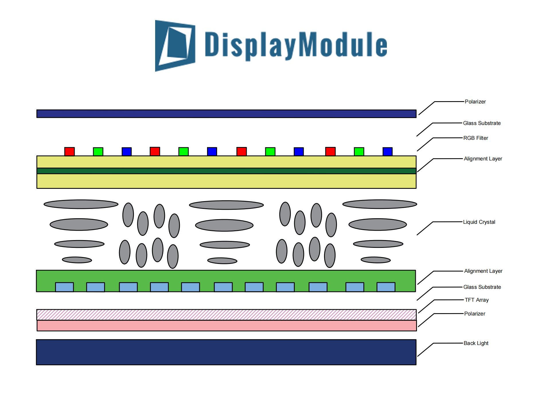
The Glass Base Layer
A common Gen 10.5 production line uses a glass sheet measuring a massive 2,940 mm by 3,370 mm, with a thickness typically around 0.5 mm (~0.02 inches). The primary material is not ordinary window glass but a special alkali-free glass, such as Corning's Eagle XG, which is designed to have a thermal expansion coefficient that closely matches that of the silicon-based layers deposited on it. This precise matching, with a typical coefficient of around 3.5 x 10⁻⁶/°C, is absolutely critical to prevent warping, cracking, or layer misalignment—errors of less than 1 micrometer can ruin a panel—when the substrate is subjected to high-temperature processing stages that can exceed 450 °C (842 °F).
The surface of this glass base is meticulously patterned with a grid of transparent conductive lines, most commonly made from Indium Tin Oxide (ITO). These lines are arranged horizontally and vertically, insulated from each other by silicon nitride or silicon dioxide layers with a thickness of about 200 to 400 nanometers. This grid defines the pixel matrix. For a standard Full High Definition (FHD) display with a resolution of 1920 x 1080 pixels, there will be 1920 vertical data lines and 1080 horizontal gate lines, creating a total of over 2 million intersections.
Each intersection defines a sub-pixel cell, which has a typical size of about 100 micrometers on each side for a 24-inch FHD monitor. Within each cell, the key elements are fabricated: the TFT switch, the transparent pixel electrode (also made of ITO), and the storage capacitor (Cs). The TFT itself is incredibly small, with a channel length that can be less than 5 micrometers. The storage capacitor, crucial for maintaining voltage stability, is designed to have a capacitance of approximately 0.5 pF, which is about 5 times larger than the inherent 0.1 pF capacitance of the liquid crystal cell (CLc) it supports.
A critical but often overlooked part of the glass base is the alignment layer. Before the liquid crystal is injected, the inner surface of the glass is coated with a thin polymer film, usually polyimide (PI), at a thickness of about 50 to 100 nm. The precision of this alignment is measured in degrees of pre-tilt, typically between 1 and 5 degrees off the surface plane, which is essential for the liquid crystals to twist in a predictable and controlled manner when a voltage is applied. Without this directional control, the molecules would scatter light randomly, leading to severe light leakage and very poor contrast ratios, potentially reducing the native contrast from a spec of 1000:1 to an unusable level below 100:1.
|
Feature |
Rear TFT Array Glass |
Front Color Filter Glass |
|---|---|---|
|
Primary Function |
Active matrix of TFTs and electrodes |
Color filtration and common electrode |
|
Key Structures |
Gate/data lines, TFTs, Pixel electrodes, Cs |
Black matrix, RGB color filters, ITO common electrode |
|
Alignment Layer |
Present, critical for LC orientation |
Present, must be rubbed perpendicular to rear layer |
|
Surface Flatness |
Extreme (Roughness < 1 nm) for TFT patterning |
Critical for uniform cell gap (e.g., 3.5 µm) |
|
Thermal Stability |
Must withstand >450°C process temperatures |
Lower temperature tolerance (typically <300°C) |
The glass must have exceptional surface flatness, with surface variations of less than 1 nanometer over large areas, to ensure that the subsequent thin-film layers are deposited uniformly. The final assembly involves precisely spacing this active glass substrate a consistent 3 to 5 micrometers away from the front color filter glass using spherical spacers, creating the cavity for the liquid crystal. This cell gap must be held to a tolerance of less than ±0.1 µm across the entire panel to guarantee uniform color and brightness, a testament to the engineering precision embodied in this foundational layer.
Semiconductor Layer Types
The active semiconductor layer is the heart of the Thin-Film Transistor, determining its speed, power consumption, and overall performance. This ultra-thin layer, typically only 30 to 200 nanometers thick, is where the crucial switching action occurs. The choice of semiconductor material directly impacts key metrics like electron mobility, measured in centimeters squared per volt-second (cm²/V·s), which can range from less than 1 cm²/V·s for basic materials to over 100 cm²/V·s for advanced compounds. This mobility defines how quickly electrons can move through the material, influencing the TFT's switching speed and its ability to drive high-resolution, fast-refresh-rate displays. The on/off current ratio, another critical parameter, must be very high, typically exceeding 10⁶ to 10⁷, to ensure the transistor can cleanly switch between a fully conducting "on" state and a near-perfect insulating "off" state, preventing charge leakage from the pixel capacitor.
For decades, the dominant material has been hydrogenated amorphous silicon (a-Si:H). The addition of hydrogen, at a concentration of about 5-15%, passifies dangling bonds in the amorphous structure, making the material suitable for semiconductor use. a-Si TFTs have an electron mobility of only about 0.5 to 1.0 cm²/V·s. This low mobility is sufficient for standard 60 Hz displays with moderate resolutions, but it becomes a limiting factor for higher performance. The manufacturing process for a-Si is well-established, involving Plasma-Enhanced Chemical Vapor Deposition (PECVD) at temperatures around 250-350°C, which keeps production costs relatively low, often 20-30% lower than more advanced alternatives.
To address the limitations of a-Si, the industry developed low-temperature polycrystalline silicon (LTPS). This process involves converting the top layer of the amorphous silicon film into a polycrystalline structure with larger grains, often using an excimer laser annealing process that heats the silicon to over 600°C for a very short duration, milliseconds or less, without damaging the underlying glass substrate. The resulting grain sizes can range from 0.1 to 0.5 micrometers. This crystalline structure offers a dramatic improvement in electron mobility, typically in the range of 50 to 100 cm²/V·s, which is about 100 times higher than a-Si. This high mobility allows for much faster switching speeds, enabling high-refresh-rate displays (120 Hz, 240 Hz, and beyond) and higher resolutions. Furthermore, the higher mobility allows the TFTs themselves to be made smaller, increasing the aperture ratio (the light-transmitting area of each pixel) by 10-20%, which improves brightness and power efficiency. The same LTPS process can also be used to integrate the driving circuitry directly onto the glass substrate, reducing the number of external chips and overall module cost by approximately 15%. The primary drawback is the higher complexity and cost of the laser crystallization process, which can increase the production cost by 20-30% compared to a-Si lines.
The Key Insulating Layer
In a TFT array, insulating layers are not passive barriers; they are active components that define the device's electrical integrity and reliability. The most critical of these is the gate insulator (GI), a thin film that electrically separates the gate electrode from the semiconductor channel. Its quality directly dictates the TFT's performance. This layer, typically made of silicon nitride (SiNx) or silicon dioxide (SiO2), has a thickness ranging from 100 to 300 nanometers. Its primary function is to form a capacitive coupling between the gate and the channel. When a gate voltage of +15 to +20 volts is applied, this capacitor creates an electric field that draws electrons, forming the conductive pathway. The insulator's quality is measured by its dielectric strength, which must be high enough to prevent electrical breakdown under this field, typically requiring a robustness of over 5 megavolts per centimeter. Even a tiny defect, like a pinhole with a diameter of just 0.1 micrometers, can create a short circuit, rendering the entire pixel useless.
The gate insulator's effectiveness is quantified by its capacitance per unit area, which is a function of its dielectric constant (k) and its thickness (d). A higher capacitance, achieved by using a material with a high k-value (like SiNx, with k ≈ 6-7) or a thinner layer, allows for a stronger channel to be induced with a lower gate voltage. This improves the TFT's switching speed and reduces power consumption. However, making the layer thinner increases the risk of leakage current and reduces the breakdown voltage. For a standard a-Si TFT, the gate insulator's capacitance is engineered to provide an optimal balance, enabling a strong on-current while keeping the off-current exceptionally low, often below 1 picoampere.
Another vital insulating layer is the one that forms the storage capacitor (Cs). As mentioned, the liquid crystal capacitor (CLc) has a value of only about 0.1 pF, which is insufficient to hold a charge for the 16.7-millisecond frame duration at a 60 Hz refresh rate. The storage capacitor Cs is added in parallel to boost the total charge-holding capacity. This capacitor is created by placing an insulating layer between two conductive electrodes, often a dedicated metal line and the pixel electrode. The capacitance of Cs is designed to be significantly larger, around 0.5 pF, which is about 5 times the capacitance of the CLc.
The insulator used for Cs, also typically a 200-300 nm layer of SiNx, must have similarly high integrity to prevent charge leakage that would defeat its purpose. The time constant (τ) of the pixel circuit, which determines how well it holds voltage, is given by the product of the total capacitance (CLc + Cs) and the effective insulation resistance. A higher Cs value directly translates to a longer τ, ensuring the pixel voltage remains stable, with a drop of less than 0.5 volts, until the next refresh cycle.
Gate, Source, and Drain
The material choice for these electrodes is critical, often involving a stack of metals like molybdenum, aluminum, and neodymium, with each layer having a precise thickness ranging from 50 to 300 nanometers to optimize conductivity, adhesion, and resistance to corrosion. The performance of the entire TFT hinges on the precise alignment and electrical isolation between these three terminals, with misalignment tolerances of less than 1 micrometer being essential to prevent short circuits and ensure consistent switching behavior across millions of transistors on a single panel.
When a positive voltage pulse, typically between +15 and +20 volts, is applied to the gate, it creates an electric field through the gate insulator. This field attracts electrons, forming a conductive channel in the semiconductor layer. The timing of this pulse is extremely precise; for a 60 Hz refresh rate on a 1080p display, each gate line is active for only about 30 microseconds per frame. The gate electrode's dimensions directly influence the TFT's switching speed. A smaller overlap capacitance between the gate and the source/drain, often designed to be less than 0.1 pF, is crucial for reducing signal delay (RC delay) along the gate line, which becomes a significant challenge in larger, higher-resolution panels.
The source electrode acts as the input, delivering the data voltage from the vertical source line (Y electrode). This voltage, which varies between 0 and 5 volts (or higher for some designs), defines the desired brightness level, or grayscale, for the pixel. When the TFT is switched on by the gate pulse, this data voltage flows from the source into the pixel. The resistance of the source line and the contact resistance between the source metal and the semiconductor layer must be minimized, ideally below 100 ohms per square, to ensure the voltage can charge the pixel capacitor quickly. The charging period is very short, often less than 10 microseconds, during which the TFT must supply enough current to raise the pixel electrode voltage to within 99% of the source voltage for accurate grayscale reproduction.
The quality of this isolation is measured by the TFT's off-state current, which must be exceptionally low—less than 1 picoampere—to prevent the charge from leaking away from the pixel capacitor during the frame time of approximately 16.7 milliseconds. Any significant leakage, even as low as 1 picoampere, would cause a noticeable voltage drop, leading to flicker or incorrect brightness.
|
Terminal |
Primary Function |
Typical Voltage Range |
Critical Parameter |
Impact on Performance |
|---|---|---|---|---|
|
Gate (X electrode) |
Switching control via electric field |
+15V to +20V (on) / 0V to -5V (off) |
Overlap Capacitance (< 0.1 pF) |
Controls row selection speed; limits maximum refresh rate. |
|
Source (Y electrode) |
Delivery of data voltage signal |
0V to 5V (Analog) |
Line Resistance (< 100 Ω/□) |
Determines pixel charging speed and accuracy; affects grayscale. |
|
Drain |
Charge transfer to pixel electrode |
Follows Source voltage when TFT is on |
Off-state Current (< 1 pA) |
Determines voltage holding ratio; prevents flicker and crosstalk. |
The relationship between these terminals creates the switching action. In the "on" state, a conductive path forms, allowing current to flow from source to drain with an effective resistance of around 10,000 to 50,000 ohms. In the "off" state, this path is broken, and the resistance between source and drain skyrockets to over 10 gigaohms, effectively creating an open circuit. This high on/off current ratio, typically exceeding 10^7, is what makes the TFT an effective switch for pixel control.
TFT Manufacturing Steps
The creation of a TFT array on a glass substrate is a highly complex, multi-stage process involving over 10-15 distinct photolithography steps, each requiring precision at the micron and sub-micron scale. The entire sequence takes place in a cleanroom environment with air cleanliness often rated at ISO Class 5 (Class 100) or better, meaning fewer than 100 particles of size 0.5 micrometers or larger per cubic foot of air.
The process begins with large "mother glass" substrates, with Gen 10.5 lines handling sheets measuring 2,940 mm x 3,370 mm (approximately 3.3 meters tall). The goal is to build a multi-layered structure of metals, insulators, and semiconductors with a total thickness of only about 1-2 micrometers, yet containing millions of perfectly functioning transistors. The production cycle time for a single panel through the array process can range from 3 to 5 days, and the overall manufacturing yield—the percentage of working panels from the total started—is a critical metric, typically ranging from 85% to 95% for mature production lines, with even a 1% improvement in yield representing millions of dollars in annual savings.
The manufacturing sequence can be broken down into a repeated pattern of film deposition, patterning, and etching. It starts with the deposition of the gate metal layer, which is typically a stack of metals like molybdenum/aluminum/molybdenum, with a total thickness of about 200-400 nanometers. This is done using a sputtering process where metal atoms are ejected from a target and deposited onto the glass in a vacuum chamber. Next, the first critical insulating layer, the gate insulator (GI), is deposited. This 100-300 nanometer thick layer of silicon nitride (SiNx) is usually applied via Plasma-Enhanced Chemical Vapor Deposition (PECVD) at temperatures around 300-400°C.
The quality of this layer is paramount; its dielectric strength must exceed 5 megavolts per centimeter to prevent electrical breakdown. Following this, the semiconductor layer is deposited. For amorphous silicon (a-Si) TFTs, this involves another PECVD step to create a layer about 30-100 nanometers thick. For metal-oxide TFTs like IGZO, a sputtering process is used with precise control over the indium, gallium, and zinc composition to achieve the desired electron mobility of 10-50 cm²/V·s.
더 읽기
OLEDs emit light via organic films (100–200nm thick) sandwiched between anode/cathode. Electrons/holes inject, merge in emissive layer, exciting molecules to release photons (100% NTSC color). No b...
I2C uses two bidirectional lines (SCL clock, SDA data) for master-slave communication. With 7/10-bit device addressing, it supports 100kHz (standard) to 3.4MHz (high-speed) modes. Start/stop condit...
댓글 남기기
이 사이트는 hCaptcha에 의해 보호되며, hCaptcha의 개인 정보 보호 정책 과 서비스 약관 이 적용됩니다.