


How PMOLEDs are Made | Manufacturing Process, Materials
PMOLED manufacturing involves ITO patterning and organic layer evaporation.
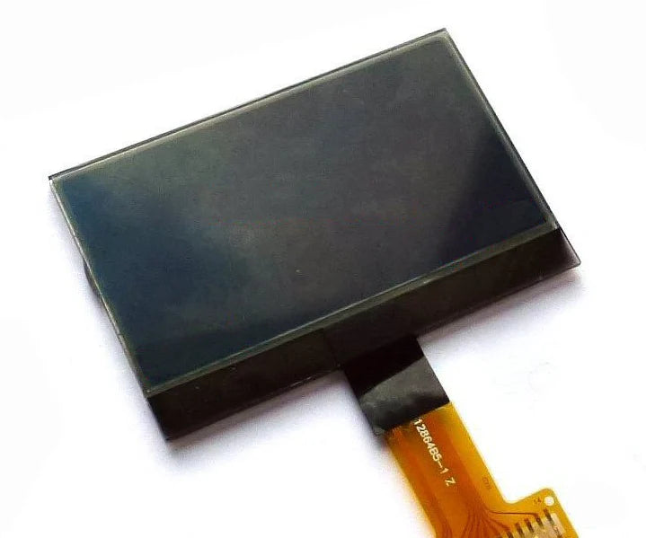
It features no TFT, relies on row and column scanning, and is suitable for small screens under 3 inches. Materials include ITO, and it achieves a contrast ratio of 10,000:1.
Manufacturing Process
PMOLED manufacturing is completed under a pressure of 10^-6 Torr, utilizing glass substrates with a thickness of 0.7 mm.
The ITO film thickness is approximately 100 to 150 nanometers, with a sheet resistance of around 15 ohms.
Pixels are formed at the intersection points of the anode and cathode, with a single-pixel response time of less than 10 microseconds.
Cathode strip separation is achieved through negative photoresist isolation pillars with a height of 1.5 micrometers, and the total thickness of the organic layers is maintained at approximately 150 nanometers.
Substrate Cleaning and Etching
Soda-lime glass with a thickness of 0.7 mm or 0.5 mm is selected as the starting substrate. Its surface is pre-covered with a layer of Indium Tin Oxide (ITO) thin film via a magnetron sputtering process.
The thickness of this film is typically set between 100 and 150 nanometers, requiring a transmittance of over 85% at a wavelength of 550 nanometers, and a sheet resistance value stabilized in the range of 10 to 15 ohms.
The first procedure on the production line is multi-stage automatic cleaning, which usually consists of 7 to 9 independent tanks for continuous operation.
The first two tanks are filled with diluted alkaline surfactant, maintained at a temperature of 50 to 60 degrees Celsius, utilizing chemical saponification to remove fingerprints, oils, and trace organic residues from the glass surface.
Subsequent tanks introduce dual-frequency ultrasonic waves at 40 kHz and 80 kHz; the alternating cavitation effects can strip particles with diameters over 1 micrometer.
To handle finer sub-micron contaminants, the system is configured with a 1 MHz high-frequency megasonic cleaning module.
The acceleration generated at this frequency effectively overcomes the Van der Waals forces between the particles and the substrate.
The water quality standard for cleaning is strictly locked at a resistivity of 18.2 MΩ·cm, with total organic carbon (TOC) content below 5 ppb.
During the final rinsing stage, multi-stage overflow ensures that the residual concentration continues to decrease, followed by entry into an isopropyl alcohol (IPA) dehydration or hot air drying system.
Dried substrates must undergo surface energy testing, where the water droplet contact angle must be reduced from the initial 30–50 degrees to below 10 degrees.
To further enhance the adhesion of subsequent organic layers, the substrate is subjected to 172 nm vacuum ultraviolet (VUV) irradiation from an excimer lamp or high-power UV-ozone treatment for 5 to 10 minutes.
This step increases the work function of the ITO surface from 4.5 eV to 4.8–5.0 eV, reducing the potential barrier height between the anode and the hole injection layer.
| Process Stage | Core Control Parameters | Measurement Indicators |
|---|---|---|
| Chemical Cleaning | 5% Concentration detergent, Temp 55°C | Particle count < 10 (above 0.5 µm) |
| Megasonic Treatment | Frequency 1 MHz, Power 800 W | Surface particle removal rate > 98% |
| Photoresist Coating | Speed 2500 to 3500 RPM | Film thickness 1.2 µm, Uniformity ± 2% |
| UV Exposure | Energy density 80 to 120 mJ | Linewidth tolerance ± 1.5 µm |
| Acidic Etching | HCl and HNO3 mixing ratio 10:1 | Etch rate 2 nm/s, Temp 45°C |
The substrate rotates at high speed on a vacuum chuck, and the photoresist is dropped into the center via a precision pump.
The rotation speed is controlled at 3000 RPM to ensure the formation of a uniform 1.2 µm thick film.
It then enters a 95°C pre-bake oven for 90 seconds to volatilize 90% of the solvent in the colloid.
The exposure machine uses 365 nm UV light to apply energy to the substrate through a customized chrome mask, with the exposure dose set at approximately 100 mJ.
The development process uses a 2.38% concentration Tetramethylammonium Hydroxide (TMAH) solution, dissolving the non-illuminated or illuminated parts within 60 seconds.
Developed substrates undergo another high-temperature hard bake at 120°C to enhance the acid resistance of the remaining photoresist.
Upon entering the chemical etching tank, the ITO film is exposed to a strong acid mixture heated to 45°C.
A typical etching solution ratio is a combination of hydrochloric acid, nitric acid, and water, with reaction time precise to the second.
Since etching is an isotropic reaction, lateral etching causes the final line width to be about 1 to 2 micrometers smaller than the mask design; therefore, compensation must be reserved during the layout design stage.
After etching, a 3% to 5% concentration sodium hydroxide solution is used as a stripping agent to thoroughly remove the surface photoresist.
The resulting anode line spacing is typically 20 to 50 micrometers, which determines the pixel density of the display.
- ITO Film Sheet Resistance: 10 to 20 ohms per square.
- Photoresist Residue Detection: Observed via Atomic Force Microscopy (AFM), height fluctuations must be less than 5 nm.
- Etch Slope Angle: Controlled between 30 and 60 degrees to prevent subsequent evaporation layers from breaking at the edges.
- Pure Water Resistivity: Constant at 18.2 MΩ·cm.
- Processing Environment: ISO Class 5 (Class 100) cleanroom, Temp 22°C, Humidity 45%.
Smooth ITO edge profiles prevent pixel electrical breakdown.
The final output substrates are stored in nitrogen-filled dry boxes, with storage time usually limited to 24 hours to prevent surface re-oxidation or adsorption of environmental organic molecules.
At the final moment before entering the evaporation chamber, a secondary oxygen plasma cleaning is implemented, with power set at 200 W and a treatment duration of 120 seconds.
Through the dual effects of physical impact and chemical oxidation, surface organic carbon residue is reduced to below 1 atomic percent.
Isolation Structure Manufacturing
Insulation films of 100 to 300 nm thickness and isolation pillars 1.5 to 3.5 µm high are used.
The insulation layer often uses silicon dioxide, produced via Plasma Enhanced Chemical Vapor Deposition (PECVD) at 250 degrees Celsius to define the light-emitting area.
Isolation pillars utilize the inverted trapezoidal cross-section characteristic of negative photoresists, with the top width being 2 to 4 µm wider than the bottom.
This physical height difference and shape design cause the subsequently evaporated cathode metal to automatically disconnect when crossing the isolation pillars, forming mutually non-interfering strip electrodes, with linewidth tolerance maintained at ±1 µm.
After completing the anode etching, the substrate surface is covered with an insulating substance known as the Pixel Definition Layer (PDL).
This layer is usually selected from silicon dioxide or silicon nitride materials and grown via PECVD equipment.
The pressure in the reaction chamber is set at approximately 1 Torr, introducing silane and ammonia for chemical reactions at 250 to 300 degrees Celsius.
The resulting film thickness is controlled at around 200 nm, with a refractive index maintained at approximately 1.9.
The role of the insulation layer is to cover the edges of the ITO anode, as etched ITO edges often have tiny burrs or steep slopes; if left uncovered, the high electric field strength at these sites would lead to breakdown of the light-emitting layer.
By coating a layer of positive photoresist and undergoing exposure/development, Reactive Ion Etching (RIE) technology is used to open rectangular or square windows in the insulation layer.
The size of these windows directly determines the effective light-emitting area of the display.
The etching gas flow typically uses a mixture of carbon tetrafluoride and oxygen at a flow ratio of 10:1.
The window edge slope angle after etching must be gentle, usually between 20 and 40 degrees, to ensure uniform coverage of subsequent organic layers.
To separate the cathode lines without using high-precision masks, it is necessary to manufacture a wall structure with an inverted trapezoidal cross-section.
High-viscosity negative photoresist, typically 20 to 50 cPs, is used for this structure.
The photoresist is dropped onto the center of the substrate and spin-coated at 1500 to 2000 RPM, resulting in a dry film thickness usually between 2.5 µm and 3 µm.
The subsequent pre-bake process is performed on a hot plate at 100°C for 120 seconds to remove over 85% of the solvent in the colloid.
- Photoresist Layer Thickness: 2.5 to 3.5 µm.
- Exposure Wavelength: 365 nm (i-line).
- Exposure Energy Density: 300 to 500 mJ/cm².
- Developer Concentration: 2.38% TMAH.
- Development Time: 90 to 120 seconds.
| Structural Parameter | Specification Index | Impact Description |
|---|---|---|
| Isolation Pillar Height | 1.5 to 3.5 µm | Height must exceed 10x the cathode evaporation thickness |
| Bottom Width | 5 to 8 µm | Determines insulation distance between cathode lines |
| Top Width | 8 to 12 µm | Top wider than bottom forms a shadowing effect |
| Taper Angle | 60 to 75 degrees (internal) | Sharper angles improve metal disconnection results |
| Line Spacing | 15 to 30 µm | Limits the screen's pixel density (PPI) |
Due to the characteristics of negative photoresist, the cross-linking reaction of the illuminated part decreases from top to bottom.
By controlling exposure dose and focal position, the cross-linking degree at the bottom is made lower than at the top, forming an "overhang" or top-heavy shape during development.
This inverted triangular shadow zone blocks the deposition path of metal atoms during subsequent evaporation.
After development, the substrate enters a high-temperature oven for a hard bake at 150 to 200°C for at least 30 minutes.
This step increases the mechanical strength and chemical stability of the isolation pillars, preventing them from releasing small-molecule organic gases in the subsequent high-vacuum evaporation environment, which would pollute the vacuum chamber.
The surface roughness of the isolation pillars must be extremely low, with an RMS roughness requirement of less than 2 nm.
If an isolation pillar collapses or breaks, it will lead to a short circuit between adjacent cathode lines.
Observed under a microscope, these isolation pillars look like rows of tiny fences spanning across the anode lines.
The alignment direction of the isolation pillars must be strictly perpendicular (90 degrees) to the ITO anode lines.
This cross structure forms the basic pixel grid of the PMOLED. At each intersection, the bottom is the ITO anode, the middle is the organic layer to be deposited, and the top is the physically separated metal cathode.
Since the height of the isolation pillar is much greater than the total thickness of the organic and metal layers (total thickness usually does not exceed 0.3 µm), metal atoms moving in straight lines in the vacuum cannot bypass the overhanging top part of the pillar, thus naturally forming independent conductive channels.
A mixture of argon and oxygen plasma is used to bombard the substrate for 60 to 100 seconds.
This operation, in addition to removing residual photoresist particles, adjusts the surface energy of the isolation pillar sidewalls, allowing them to exhibit good physical affinity when in contact with organic vapors.
Substrates treated this way must be transferred to the evaporation equipment within 12 hours.
At this point, the substrate already possesses a complete circuit addressing framework, waiting only for the filling of light-emitting materials.
The particle count of the entire processing environment is strictly limited; particles larger than 0.5 µm must not exceed 10 per cubic foot, as any tiny defect on the isolation pillar will lead to the failure of an entire cathode line.
Multi-layer Thin Film Evaporation
The pressure inside the vacuum chamber must be pumped down to between 10^-6 and 10^-7 Torr, which is the prerequisite for ensuring organic molecules do not collide with air molecules during their motion.
The substrate is mounted on a rotating rack, with the rotation speed kept at 10 to 20 RPM to ensure deposition uniformity.
Heating sources use crucibles made of tantalum, molybdenum, or tungsten, with materials sublimated by current heating.
The sublimation temperature of organic materials is in the range of 200 to 450 degrees Celsius, and the evaporation rate is monitored in real-time via quartz crystal oscillators and fed back to the power control system.
The first layer deposited is the Hole Injection Layer (HIL), with a thickness typically between 15 and 40 nanometers.
Commonly used materials include Copper Phthalocyanine (CuPc) or polythiophene derivatives.
The role of this layer is to reduce the hole injection barrier between the ITO anode and the organic layers, allowing charges to enter the organic system smoothly.
Controlling the injection layer thickness deviation within ±1 nm prevents the risk of breakdown caused by excessive local electric fields.
This is followed by a Hole Transport Layer (HTL) with a thickness of 30 to 60 nanometers, common materials being NPB or TPD.
| Layer Name | Common Materials | Typical Thickness (nm) | Evap Rate (Å/s) | Evap Temp (°C) |
|---|---|---|---|---|
| Hole Injection Layer (HIL) | CuPc, 2-TNATA | 20 to 35 | 0.5 to 1.0 | 380 to 420 |
| Hole Transport Layer (HTL) | NPB, TPD | 40 to 55 | 1.0 to 2.0 | 260 to 300 |
| Emissive Layer (EML) | Alq3 (Host) + Dopants | 25 to 40 | 1.0 (Host) | 280 to 350 |
| Electron Transport Layer (ETL) | Alq3, BCP | 20 to 45 | 1.0 to 1.5 | 280 to 320 |
| Electron Injection Layer (EIL) | LiF | 0.5 to 1.0 | 0.1 to 0.2 | 550 to 600 |
| Metal Cathode (Cathode) | Al, Mg/Ag | 100 to 150 | 5.0 to 15.0 | 1000 to 1200 |
The Emissive Layer (EML) is the energy conversion center of the organic electroluminescent device, with a thickness typically between 20 and 45 nanometers.
It usually employs a scheme of host material doped with guest materials; host materials like CBP or Alq3, and guest materials like fluorescent or phosphorescent molecules with high luminous efficiency.
The doping ratio is strictly limited between 0.5% and 10%; concentrations too high or too low will trigger quenching, leading to a decline in luminous efficiency.
Two evaporation sources are turned on simultaneously for co-evaporation, with their respective powers adjusted to maintain precise doping ratios.
For example, in producing a green PMOLED, the evaporation rate of the host material Alq3 is set at 1 Å/s, while the guest material C545T is controlled at 0.01 Å/s.
Above the emissive layer, the Electron Transport Layer (ETL) is responsible for guiding electrons from the cathode to the emissive layer.
This layer's thickness is 20 to 40 nm, and the material needs to have a low LUMO level for electron injection.
Alq3 can serve as both the emissive layer host and the electron transport layer.
To further enhance electron injection efficiency, an extremely thin Electron Injection Layer (EIL) is added before the metal cathode deposition, usually 0.5 to 1 nm thick Lithium Fluoride (LiF).
"The shutter baffles inside the evaporation chamber must be cleaned regularly to prevent accumulated organic residues from producing peeling particles."
Because pre-fabricated isolation pillars already exist in the PMOLED structure, metal aluminum or magnesium-silver alloys will be automatically physically separated during evaporation.
The aluminum cathode thickness is typically set above 100 nm to ensure sufficient conductivity and reflectivity, reflecting the light emitted backward from the emissive layer toward the observer.
Metal evaporation sources usually employ high-power electron beam evaporation or high-current resistance heating, with rates at 5 to 10 Å/s to reduce thermal damage to the underlying organic layers.
The cumulative thickness of the entire multi-layer structure usually does not exceed 300 nm, and the flatness of each interface affects the final display quality.
The quartz crystal monitor is the "eye" of this process; its oscillation frequency decreases as the deposited mass increases.
The system calculates instantaneous thickness and rate through frequency change.
To ensure stability during the hours-long production process, the evaporation source chambers use a dual-cycle water cooling system to keep the external environment temperature constant at around 20 degrees Celsius.
- Film Uniformity: Within a 370 x 470 mm substrate, thickness fluctuations must be less than 3%.
- Cross-contamination Control: Vacuum locks are set between different chambers to prevent hole materials and electron materials from mixing.
- Material Utilization: Spray nozzle design is optimized so expensive organic materials deposit on the substrate rather than chamber walls.
- Substrate Temp Control: Substrate temperature must remain below 80°C during evaporation to prevent crystallization or morphological changes in the organic film.
The luminous lifespan of each color is closely related to material stability.
Blue materials, due to their large energy gaps, often degrade more easily than red or green materials.
In actual production, adding an exciton blocking layer can prevent excitons from diffusing to electrode interfaces, improving the operational stability of the device.
Materials
The PMOLED construction relies on soda-lime glass or polyimide (PI) substrates of 0.5 to 0.7 mm thickness.
The ITO anode layer thickness is set at 100 to 150 nanometers, with sheet resistance maintained at around 10 ohms.
Light-emitting hosts such as Alq3 are doped with 1% fluorescent dye, combined with a 40 nm thick NPB hole transport layer.
The cathode chooses 200 nm aluminum, with a work function of about 4.2 eV, adapted to a pulse drive voltage of 12 V to 20 V.
Substrate & Transparent Conductive Layer
PMOLED production begins with strict screening of substrate materials.
Typical glass substrate thickness ranges from 0.5 mm to 1.1 mm, with the 0.7 mm specification being the most common.
Soda-lime glass is widely used due to cost advantages, but it contains alkali metal ions that easily migrate into the organic layers under an electric field, leading to device failure.
Therefore, the glass surface must be pre-covered with a silicon dioxide (SiO2) barrier layer of about 20 nm to 30 nm thickness to prevent sodium ion penetration.
In contrast, borosilicate glass has a lower thermal expansion coefficient, about 3.2 to 3.8 * 10^-6 / K, maintaining better dimensional stability during subsequent heating processes over 200°C and reducing electrode alignment deviation caused by thermal expansion/contraction.
| Physical Parameter | Soda-lime Glass Spec | Borosilicate Glass Spec | Alkali-free Glass Spec |
|---|---|---|---|
| Thickness (mm) | 0.7 / 1.1 | 0.5 / 0.7 | 0.4 / 0.5 |
| Transmittance (%) | > 90 (at 550nm) | > 91 (at 550nm) | > 92 (at 550nm) |
| Surface Roughness Ra (nm) | < 1.0 | < 0.8 | < 0.5 |
| Softening Point (℃) | 720 - 740 | 820 - 850 | 950 - 980 |
| Refractive Index (nD) | 1.51 - 1.52 | 1.47 - 1.48 | 1.50 - 1.51 |
Indium Tin Oxide (ITO) is usually chosen for the transparent conductive film; it is a wide-bandgap semiconductor material, with an indium-to-tin atomic ratio typically controlled at around 90:10.
In PMOLED structures, the sheet resistance of the ITO film must be maintained at 10 to 15 ohms per square.
To achieve this conductivity, the physical thickness of the ITO is typically deposited at 120 to 150 nm.
The ITO film is prepared by DC magnetron sputtering, with chamber pressure controlled at 0.3 to 0.8 Pa, introducing argon as the sputtering gas mixed with 1% to 3% oxygen to precisely regulate carrier concentration.
Minute changes in oxygen content significantly affect the work function; ideally, the PMOLED anode work function should be between 4.7 eV and 4.9 eV to match the HOMO level of the hole injection layer.
- ITO Deposition Parameters: Sputtering power density is maintained at 1.5 W/cm² to 2.5 W/cm², with substrates heated to 200–300°C to promote crystallization.
- Etching Precision: Anode line width is typically 50 to 200 µm, with a gap of 10 to 30 µm. Etch bias must be controlled under 1 µm to prevent a significant reduction in effective light-emitting area.
- Photoresist Specifications: Positive diazonaphthoquinone (DNQ) photoresist is used, coating thickness 1.2 to 1.8 µm, pre-bake at 90°C, development time 40–60 seconds.
- Chemical Thinning & Polishing: Glass substrates undergo Chemical Mechanical Polishing (CMP) before entering the line, ensuring local Peak-to-Valley height is less than 10 nm; any particle over 20 nm will cause uneven organic film formation.
The etching solution's main component is oxalic acid (5%–10% concentration) or a mixture of HCl and HNO3.
For amorphous ITO (a-ITO), etching is fast with neat edges, but a-ITO transforms to polycrystalline during heat treatment before organic film evaporation, leading to stress-induced cracks.
High-end PMOLEDs prefer polycrystalline ITO, requiring high-temperature annealing at 230°C for 60 minutes after etching to distribute grain size evenly between 30 and 50 nm, enhancing film chemical stability and corrosion resistance.
| Etch/Cleaning Stage | Chemical Agent / Energy Level | Processing Time | Expected Result |
|---|---|---|---|
| ITO Etching | 5% Oxalic Acid (35℃) | 120 - 180 seconds | Clear strip column electrodes |
| PR Stripping | Potassium Hydroxide (KOH) | 60 - 90 seconds | Complete removal of residual PR |
| Ultrasonic Cleaning | DI Water (18 MΩ.cm) | 5 - 10 minutes | Removal of sub-micron dust particles |
| UV-Ozone Treatment | 185nm & 254nm UV light | 5 - 15 minutes | Increased surface oxygen/work function |
| Plasma Cleaning | Oxygen Plasma (150W) | 1 - 3 minutes | Organic removal, improved wettability |
The production line typically adopts a multi-stage continuous cleaning system.
The first step uses 40 kHz and 80 kHz dual-frequency ultrasonics in a detergent solution to remove oil.
Then, rinsing is done with DI water at 10 L/min, ensuring resistivity is above 18 MΩ·cm.
Dried substrates must immediately undergo UV-Ozone or oxygen plasma treatment.
The active energy from UV-Ozone breaks residual carbon chains, reducing surface carbon to below 5%.
Simultaneously, oxygen atoms fill oxygen vacancies in the ITO lattice, aligning surface dipoles and increasing the work function from 4.5 eV to 4.8 eV, directly lowering the turn-on voltage.
Flexible PMOLED substrates use Polyimide (PI) film. PI slurry is coated on carrier glass via slot-die coating to form a 10 to 20 µm film.
Since PI is non-conductive, a high-adhesion metal transition layer or direct low-temp ITO sputtering is required.
Flexible substrates easily undergo 0.1% to 0.2% dimensional shrinkage when heated, requiring compensation factors in mask design.
PI's glass transition temperature (Tg) must be higher than 350°C to withstand radiation heat from VTE sources.
Molecular-level Organic Stacking
The total thickness of the organic stack is usually maintained between 100 nm and 150 nm—about 1/500th the diameter of a human hair.
To ensure effective charge hopping between molecules, the chamber vacuum must be below 1.33 * 10^-5 Pa to prevent residual oxygen or water from oxidizing organic molecules.
Thickness control precision for each functional layer is at the 0.1 nm level, relying on quartz crystal oscillators to monitor deposition rates (typically 0.1 Å/s to 1.0 Å/s).
The first layer from the anode up is the Hole Injection Layer (HIL), about 10 to 30 nm thick.
Common materials are Copper Phthalocyanine (CuPc) or highly conductive polymers.
CuPc's HOMO is ~5.2 eV, between ITO's 4.8 eV and the HTL's 5.4 eV, forming a stepped energy alignment.
This reduces the barrier for holes entering the organic system, allowing start-up at 3–4 V.
Following is the Hole Transport Layer (HTL), 30 to 60 nm thick, with NPB being the mainstream material.
NPB's hole mobility reaches 10^-4 cm²/Vs, ensuring fast hole movement to the EML.
To prevent electrons from passing the EML into the HTL, HTL materials have high LUMOs (~2.3 eV) to act as electron blockers.
The Emissive Layer (EML) is the most complex area in the molecular stack, 20 to 40 nm thick. PMOLEDs often use a "guest-host" system: a host material and fluorescent dopants.
For green light, Alq3 is a common host, with Coumarin 6 or C545T as dopants.
Doping ratios must be precisely 1%–3% by mass.
High concentrations cause self-quenching due to molecular proximity; low concentrations drop exciton capture efficiency and color purity.
In the EML, holes and electrons form excitons, and energy transfers from host to guest via Förster resonance energy transfer, releasing photons.
| Functional Layer | Typical Thickness (nm) | Common Chemical Material | HOMO/LUMO (eV) | Mobility (cm2/Vs) |
|---|---|---|---|---|
| HIL | 15 - 25 | CuPc | 5.2 / 2.7 | 10^-7 |
| HTL | 40 - 55 | NPB | 5.4 / 2.3 | 10^-4 |
| EML | 20 - 35 | Alq3:C545T | 5.7 / 3.0 | 10^-6 |
| ETL | 25 - 45 | Alq3 | 5.8 / 3.1 | 10^-6 |
| EIL | 0.5 - 1.0 | LiF | Ultra-thin tunneling | N/A |
The Electron Transport Layer (ETL) is above the EML, about 30 nm thick.
Alq3 is an excellent ETL material with stable chemical properties.
ETL molecular structures require high electron affinity to receive electrons from the cathode.
Since organic electron mobility is generally lower than hole mobility, ETL thickness is increased or high-mobility materials like BCP are used to balance the recombination center at the EML's geometric center.
Between the ETL and cathode is the Electron Injection Layer (EIL), 0.5 to 1 nm thick—almost atomic coverage.
Lithium Fluoride (LiF) is the standard EIL; it reacts at the aluminum interface, lowering the work function and boosting injection efficiency by over 10x.
- Deposition Temp Precision: Temp fluctuations must be within ±0.5°C to prevent decomposition or film thickness deviation.
- Mask Alignment Distance: The gap between the Fine Metal Mask (FMM) and substrate must be under 50 µm to reduce Shadow Effects on pixel edges.
- Material Purity: Organic monomers must undergo at least three sublimations; impurities must be below 10 ppb to prevent charge trapping.
- Interface Thermal Stability: Tg of materials must be above 100°C to ensure molecular alignment doesn't recrystallize under high pulse currents.
When 12 V to 18 V pulse drive voltage is applied, carriers overcome barrier heights to form stable current density in the EML.
To improve light extraction, functional layer thicknesses are adjusted via optical interference so the distance from the EML center to the reflective cathode matches 1/4 wavelength (Micro-cavity Effect).
This narrows the FWHM of the spectrum, making colors more saturated and increasing brightness by over 15% at the same current.
Charge Injection Metal Properties
Cathodes consist of low-work-function metals to match the ETL's LUMO.
In standard PMOLEDs, total cathode thickness is 150 to 250 nm.
To lower the barrier, an auxiliary layer is deposited first rather than bulk metal.
LiF is the most common EIL material, thickness 0.5 to 1.2 nm.
Although an insulator, electrons pass through via quantum tunneling at thickness < 2 nm.
Al deposition on LiF lowers the effective work function from 4.2 eV to ~3.0 eV, lowering turn-on voltage by 0.5 to 1.5 V.
| Metal/Alloy Type | Work Function (eV) | Visible Reflectivity (%) | Resistivity (uΩ·cm) | CTE (10^-6/K) |
|---|---|---|---|---|
| Aluminum (Al) | 4.28 | 90 - 92 | 2.65 | 23.1 |
| Mg:Ag Alloy | 3.7 (10:1 ratio) | 85 - 88 | 4.5 - 6.0 | 19.5 |
| Calcium (Ca) | 2.87 | 70 - 75 | 3.91 | 22.3 |
| Silver (Ag) | 4.26 | 96 - 98 | 1.59 | 18.9 |
| Lithium (Li) | 2.93 | 60 - 65 | 9.28 | 46.0 |
PMOLED is a bottom-emitting structure; light passes the ITO to exit from the glass side.
The cathode must act as a "mirror." Aluminum's reflectivity at 550 nm is > 90%.
However, Al has high internal stress; over 300 nm, it easily cracks or peels.
Mg:Ag alloys are sometimes used for better adhesion.
Magnesium's low work function (3.7 eV) aids injection but it's unstable in air; 10% Silver is added to form a stable alloy film while maintaining low work function.
- Deposition Rate Control: Cathode deposition is 5 to 15 Å/s. High speeds cause bond breaking via high kinetic energy; low speeds allow residual gas doping, increasing resistance.
- Mask Deformation: Cathode strips are formed by FMMs perpendicular to the ITO. As sources are > 1000°C, masks absorb radiation heat. Mask CTE must be < 1.2 * 10^-6 / K to prevent pixel shift.
- Barrier Height: Injection barrier = Metal Work Function - ETL LUMO. For Alq3 (LUMO ~3.1 eV), LiF/Al lowers the barrier to < 0.2 eV.
- Pulse Current Tolerance: Single-row cathodes carry the sum of all pixel currents during scanning. Strip resistance must be low; a 3 cm cathode strip must be < 5 ohms to prevent brightness non-uniformity.
The mean free path of metal atoms must exceed the distance to the substrate; vacuum must be better than 5 * 10^-4 Pa.
Substrates rotate during evaporation to keep uniformity errors < 3%.
Non-uniform thickness causes rainbow patterns (iridescence) due to reflection phase differences.
Deposition is exothermic; local substrate temp can rise to 60–80°C.
Backplane cooling (He gas or water cycle) locks substrates below 40°C to prevent organic recrystallization.
During ITO patterning, anode edges form slopes. If the cathode thins too much over these slopes, high resistance zones form.
Multi-point sources ensure > 80% coverage on 3D steps.
Metal diffusion into the EML is strictly limited to prevent non-radiative recombination (quenching), which decays efficiency by 0.1%–0.5% per hour, shortening life.
| Process Parameter | Setting Range | Performance Impact |
|---|---|---|
| Vacuum (Pa) | 1.0*10^-5 to 5.0*10^-4 | Film purity and mobility |
| Deposition Rate (A/s) | 3.0 - 12.0 | Thermal damage and cycle time |
| Substrate Dist (mm) | 400 - 600 | Uniformity and material usage |
| LiF Evap Temp (℃) | 800 - 850 | Nucleation density of ultra-thin layers |
| Al Evap Temp (℃) | 1100 - 1250 | Vapor pressure and flux |
Aluminum atoms form a 2–5 nm self-passivating Al2O3 layer in air, but this doesn't block moisture.
Cathode strips are designed 10–20 µm wider than anodes to tolerate etching/alignment errors.
Metal purity must be > 99.999%; traces of Cu or Fe lead to electromigration and shorts.
For high contrast, a black absorbing layer is added above the Al cathode to drop ambient reflection from 90% to < 5%.
Environmental Isolation Packaging
To ensure > 10,000 hours of stable operation, the encapsulation must reach a Water Vapor Transmission Rate (WVTR) of 10^-6 g/m²/day—five orders of magnitude higher than LCD requirements.
Moisture reacts with LiF or Al to produce Hydrogen, causing electrode detachment.
Primary components are Borosilicate glass caps or stainless steel.
Glass caps (0.5–0.7 mm) have a 0.3–0.4 mm cavity etched or sandblasted to house desiccants and prevent the cap from touching fragile organic layers.
Cap edge flatness is kept under 5 µm for uniform sealant distribution.
Metal caps have zero permeability but higher CTE (17 * 10^-6 / K) compared to glass (3.8 * 10^-6 / K).
Sealants are UV-curable epoxies, solidifying in 30–60s under 365 nm light.
Width is set at 0.8–1.5 mm, thickness 10–20 µm.
Narrower paths shorten life; wider paths reduce bezel-to-screen ratio.
Viscosity is 50,000–100,000 cPs for high-pressure dispensing without breaks.
Cured epoxy Tg must be > 90°C to maintain strength at high temps.
Common materials are Calcium Oxide (CaO) or Barium Oxide (BaO).
These absorb water irreversibly to form hydroxides. One gram of CaO absorbs 0.32g of water.
Desiccants are attached as patches in the cap cavity or screen-printed.
Thickness is 100–200 µm. Volume can expand 1.5–2x after absorption.
The glovebox dew point must be below -80°C, with Oxygen and moisture < 1 ppm.
Lidding is done at 1.1 atm (positive pressure) to help the sealant fill minute glass defects.
Standard accelerated aging is the 85/85 test (85°C/85% RH) for 500 hours.
Good designs keep light-emitting area decay < 2%. Thermal cycling (-40°C to 90°C) verifies fatigue resistance.
For ultra-thin flexible PMOLEDs, Thin Film Encapsulation (TFE) replaces glass.
TFE uses 3–5 alternating inorganic/organic layers.
Inorganics (SiNx or Al2O3) grown via PECVD or ALD (50–100 nm) block moisture.
Organic polymers (~5 µm) buffer stress and cover particles.
Volatile Organic Compounds (VOCs) from sealants must be minimized; residuals cause quenching if they penetrate.
Data shows VOCs > 50 ppm drop initial brightness by > 10% instantly.
Read more
COG (Chip-On-Glass) technology utilizes Anisotropic Conductive Film (ACF) to directly bond driver ICs onto the LCD glass substrate through thermal ultrasonic or heat-pressure processes. The core of...
Micro OLED features 3000+ PPI and 5000 nit brightness, completely eliminating the screen-door effect; The 0.01 ms ultra-fast response time solves motion sickness, serving as the performance benchma...
Leave a comment
This site is protected by hCaptcha and the hCaptcha Privacy Policy and Terms of Service apply.