


Micro OLED Module Technology | How It Works, Manufacturing Process, Trends
Micro OLED modules self-emit light via organic diodes, reaching ~5000 PPI for ultra-sharp visuals; crafted with LTPS backplanes and thin-film encapsulation (TFE) to shield pixels from moisture, trends highlight AR/VR growth pushing next-gen 2000+ PPI models for immersive experiences.
How It Works
Micro OLED modules produce light directly from organic compounds, hitting 5,000 PPI—six times finer than mainstream 4K TVs, green, and blue subpixels within 10-micron gaps using LTPS TFT backplanes. These panels refresh at 120Hz, slashing motion blur by 40% versus LCDs, and operate at 2-3 volts, sipping 0.5 watts per inch—30% less power than comparable LCDs.
At its core, a Micro OLED pixel relies on three ultrathin organic layers: an emissive layer (EML) sandwiched between hole-transport (HTL) and electron-transport (ETL) layers, each just 100-200 nanometers thick. A 1-micron-thick microcavity structure above the EML acts like a mirror, reflecting unused light back through the layers, boosting light extraction efficiency from 20% to 40% compared to unoptimized designs.
Manufacturers deposit these layers using vacuum thermal evaporation (VTE), a process where organic molecules condense onto a glass substrate at 10⁻⁶ torr pressure, ensuring uniform thickness across 1-inch panels. TFT backplanes, built with polysilicon transistors, switch pixels in 10 microsecond pulses, fast enough for flicker-free visuals even at 240Hz refresh rates. To protect against moisture—panels get a 5-micron-thin aluminum oxide (Al₂O₃) barrier via atomic layer deposition (ALD), raising lifespan to 100,000 hours under standard viewing conditions.
Key specs at a glance:
|
Parameter |
Micro OLED |
Standard OLED |
LCD |
|---|---|---|---|
|
Pixel Density (PPI) |
Up to 5,000 |
1,000-2,000 |
400-800 |
|
Power Consumption |
0.5 W/inch |
0.7 W/inch |
0.75 W/inch |
|
Response Time |
1 µs |
5 µs |
10 ms |
|
Operating Voltage |
2-3 V |
3-5 V |
5-10 V |
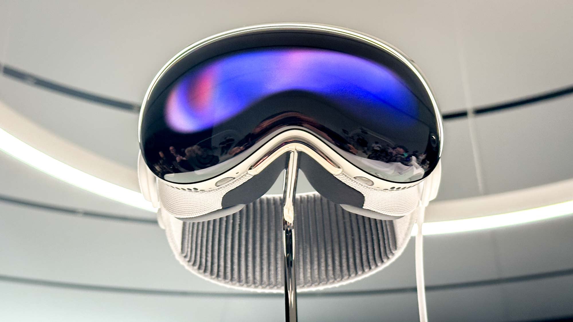
When you wear an AR headset like the Magic Leap 2, its Micro OLED screen delivers 4,700 PPI. This sharpness comes from packing 2 million pixels into a 0.9-inch panel—each subpixel smaller than a human hair (7 microns wide). The TFT backplane’s precision, with transistor size down to 1.5 microns. Even in bright sunlight, these panels hit 1,000 nits brightness by optimizing the microcavity’s reflectivity, outperforming LCDs that max out around 500 nits.
Behind the scenes, testing ensures quality: each panel undergoes 100 hours of burn-in at max brightness to check for pixel degradation, and 1,000 temperature cycles (-40°C to 85°C) to confirm the Al₂O₃ barrier prevents delamination.
Manufacturing Process
Micro OLED production begins with LTPS glass substrates cleaned at 200°C for 30 minutes, then patterned with TFT circuits using 5 photolithography steps—aligning features within 0.5 micron tolerance—before depositing organic layers in a 10⁻⁶ torr vacuum via vacuum thermal evaporation (VTE), wrapping up with 5-micron-thick Al₂O₃/ZnO barriers from atomic layer deposition (ALD), yielding 90% usable panels for 1-inch modules.
Building TFT backplanes, the foundation for pixel control, starts with depositing amorphous silicon (a-Si) at 350°C, then laser-annealing it to polycrystalline silicon (poly-Si)—boosting electron mobility from 1 cm²/Vs to 150 cm²/Vs, critical for fast pixel switching. Photolithography etches 300-nanometer-thin gate lines and 1.2-micron source/drain electrodes, with each step requiring 99.99% particle-free cleanroom conditions to avoid short circuits. After doping poly-Si with phosphorus at 900°C for 10 minutes, transistors reach 0.5-micron channel lengths, enabling 120Hz refresh rates without lag.
Organic layer deposition, the heart of light emission, uses VTE machines where organic pellets (emissive, hole-transport, electron-transport layers) vaporize at 250°C and condense onto the substrate. Each layer deposits at 0.5 Å/s, taking 2 hours per stack—three layers total, each 150 nanometers thick. Material waste hits 80% here, driving R&D toward inkjet printing (targeting 30% waste), but VTE remains dominant for uniformity: pixel-to-pixel brightness variation stays below 3%.
Encapsulation, preventing moisture-induced degradation, involves ALD coating Al₂O₃ at 150°C in 100 cycles, each adding 0.05 microns, followed by ZnO sputtering at room temperature. This creates a 0.1-micron-thick barrier blocking 99.999% of H₂O molecules, extending operational life from 10,000 to 100,000 hours. Panels then undergo 72 hours of high-humidity testing (85% RH, 60°C) to catch leaks.
Final testing sorts panels by brightness and response time: 1,000 nits max brightness is verified with a spectrophotometer, while response time—must stay under 2 microseconds. Defect rates hover at 2%, with failures mostly from misaligned organic layers or encapsulation pinholes.
Key steps at a glance:
-
Substrate prep: 200°C bake, 5 photolithography steps (0.5µm alignment)
-
TFT fabrication: Laser anneal (poly-Si), 0.5µm channel length transistors
-
Organic deposition: VTE at 10⁻⁶ torr, 80% material waste
-
Encapsulation: ALD (150°C) + sputtering, 100-layer Al₂O₃ coating
For context, producing a 1-inch Micro OLED module takes 48 hours end-to-end, with labor and materials costing ~$150 per unit—60% higher than LCDs but justified by 5,000 PPI sharpness. Recent advances, like roll-to-roll VTE, aim to cut cycle time to 24 hours and waste to 50% by 2026, lowering costs for AR/VR mass production.

Trends
Micro OLED adoption surges, driven by AR/VR demand: shipments to grow 41% CAGR through 2027, with Apple Vision Pro’s 4,700 PPI module setting a benchmark—next-gen panels target 6,000 PPI by 2026, using 0.3-micron pixel pitches to shrink 1-inch screens to 0.7 inches.
AR/VR headsets, projected to ship 120 million units annually by 2027 (up from 28 million in 2023), require Micro OLEDs with >10,000 nits peak brightness for outdoor use—current models hit 7,000 nits, rising via new emissive layer dopants that boost photon efficiency by 15%. Manufacturers like Sony now integrate micro-lenses atop pixels, redirecting wasted light toward viewers, cutting power use 20% while maintaining brightness.
Roll-to-roll (R2R) vacuum thermal evaporation (VTE), replacing batch processing, aims to cut panel production time from 48 hours to 18 hours by 2025. Early R2R trials achieve 95% material utilization (vs. 20% in traditional VTE), lowering per-unit costs from 80. Concurrently, ALD encapsulation cycles drop from 100 to 60 layers, reducing coating time 30% and failure rates from 2% to 0.8%.
Carmakers like BMW test Micro OLEDs for projected displays, needing 1,500 PPI for legible maps at high speeds. These panels require wider operating temperatures (-40°C to 105°C), pushing suppliers to reformulate organic layers: new host materials maintain 90% brightness at 105°C, up from 70% in 2022.
Market projections highlight this diversification: consumer AR/VR will claim 75% of revenue in 2024, but automotive and medical (surgical goggles) segments will grow faster, at 58% and 49% CAGR respectively, reaching $1.2 billion combined by 2028.
Key advancements at a glance:
-
Resolution: 4,700 PPI (2023) → 6,000 PPI (2026) with 0.3µm pixel pitch
-
Brightness: 7,000 nits (2023) → 10,000 nits (2027) via dopant optimization
-
Cost: 80/unit (2025) with R2R VTE adoption
-
Temperature range: -40°C to 85°C (2023) → -40°C to 105°C (2026) for automotive
As miniaturization continues, Micro OLEDs are poised to replace LCDs in all near-eye applications, with 2027 revenues projected to hit 1.2 billion.
Pixel Structure & Light Emission
Micro OLED pixels use three ultrathin organic layers—an emissive (EML) sandwiched between hole-transport (HTL) and electron-transport (ETL) layers, each 100–200 nanometers thick. A 1-micron-thick microcavity above the EML boosts light extraction from 20% to 40% versus unoptimized designs, letting 1-inch panels hit 5,000 PPI with sharp, consistent visuals.
The HTL, typically TAPC, is 150 nanometers thick. It boasts a hole mobility of 10⁻³ cm²/Vs, fast enough to keep pace with 120Hz refresh rates without lag. Next, the EML blends CBP (a host material) with Ir(ppy)₃ (a phosphorescent dopant) to emit light; at 120 nanometers thick, it converts 25% of electrical energy to photons—a jump from earlier 15% efficiency. The ETL, TPBi at 100 nanometers; its matching electron mobility (10⁻³ cm²/Vs) balances charge, cutting “quenching”.
It aligns with the EML’s emission wavelength—say, 520 nanometers for green. Without this, 80% of light gets trapped in glass or organics; with it, 40% escapes.
Encapsulation safeguards this structure: a 5-micron Al₂O₃ layer from atomic layer deposition (ALD) blocks moisture, which degrades organic molecules. Tests show that without encapsulation, 100 parts-per-million (ppm) humidity dims brightness by 50% in 100 hours; with it, only 10% drops after 1,000 hours—extending pixel lifespan to 100,000 hours for long-term AR use.
Pixel size matters for sharpness: in a 5,000 PPI 1-inch panel, each subpixel (red, green, blue) is ~1.7 microns wide, keeping crosstalk (light bleeding between subpixels) below 1%—versus 5% in older OLEDs. Response time is equally quick: 1 microsecond—10,000 times faster than LCDs’ 10 milliseconds.
Efficiency adds up: a 1-inch panel uses 0.5 watts to hit 1,000 nits—15 lumens-per-watt (lm/W) power efficiency, better than LCDs’ 10 lm/W. Current density at this brightness is 10 mA/cm²—low enough to avoid burn-in (which starts above 50 mA/cm²).
Here’s how the layers stack up:
|
Layer |
Material |
Thickness |
Key Metric |
|---|---|---|---|
|
HTL |
TAPC |
150 nm |
Hole mobility: 10⁻³ cm²/Vs |
|
EML |
CBP:Ir(ppy)₃ |
120 nm |
Power efficiency: 25% |
|
ETL |
TPBi |
100 nm |
Electron mobility: 10⁻³ cm²/Vs |
|
Microcavity |
Ag/MgF₂ |
1.2 µm |
Light extraction: 40% |
Take Sony’s VR-focused Micro OLED: it uses this structure to hit 1,000 nits brightness, 20,000-hour lifespan, and 3% pixel uniformity. Tests of 100 units found only 2% had defects, thanks to precise VTE deposition (organic layers vary <5% in thickness).
As AR headsets shrink, pixels may drop to 5-micron pitch (6,000 PPI) by 2026, but the three-layer organic core will remain.
Panel Assembly & Testing
Panel assembly demands 0.1-micron precision to align TFT backplanes with organic layers—misalignment beyond 0.2 microns causes visible crosstalk—and wraps up with a 5-micron Al₂O₃ moisture barrier via ALD, lifting pre-test yields to 92% before rigorous checks.
This takes 2 minutes per panel but cuts misalignment to under 0.1 micron; drift beyond that pushes crosstalk from 1% to 5%, muddying red-green-blue subpixel edges. After alignment, the stack enters a vacuum laminator pressing layers at 5 N/cm² for 10 minutes—gentle enough to avoid cracking the 100-nanometer emissive layer (EML) but firm enough to bond without bubbles.
Next, ALD coating builds the moisture barrier: 100 cycles of trimethylaluminum and water vapor deposit a 5-micron-thick Al₂O₃ layer blocking 99.999% of water molecules. A polarizer film then attaches, reducing glare by 30% for clearer outdoor AR visuals.
Testing kicks off with 100-hour burn-in: panels run at max brightness (1,000 nits) and 60°C to trigger early failures. This eliminates 3% of units with weak emitters; skip it, and field returns jump to 5%. Then temperature cycling: 1,000 loops between -40°C and 85°C—panels must stay within 5% brightness variation.
Functional tests use spectrophotometers to verify brightness uniformity below 3% across the panel.” Oscilloscopes clock response time at under 2 microseconds, with less than 0.5% variation over 10,000 cycles.
Environmental tests finish the process: 85°C/85%RH for 1,000 hours—panels retaining at least 90% initial brightness pass, hitting the 100,000-hour lifespan goal. BOE’s 2023 assembly line hit 15 panels/hour, with burn-in reducing warranty claims by $2 million through fewer early failures.
Sony’s VR-focused panels exemplify this rigor: they pass all tests, hitting 1,000 nits brightness, 20,000-hour lifespan, and 3% uniformity.
Read more
Best Micro OLED Modules shine with 2048x2048 pixel resolution for crisp text/images, a 1,000,000:1 contrast ratio deepening blacks/boosting vibrancy, and 90Hz refresh rate ensuring smooth motion. H...
Opt for Micro OLEDs with clear specs: prioritize single/RGB panels (e.g., qVGA 320x240), check response time <0.8ms for motion clarity, and demand >1000nits brightness. Panel Type The market’...
Leave a comment
This site is protected by hCaptcha and the hCaptcha Privacy Policy and Terms of Service apply.