


OLED Screen Module Design | Flexible Substrates, Color Gamut & Durability
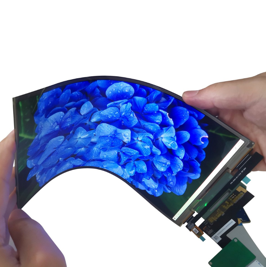
Flexible Substrates
Using Polyimide (PI) or Ultra-Thin Glass (UTG), PI substrates are 50-125μm thick with a bending radius of 1-3mm (e.g., Samsung Z Fold series), temperature resistance from -269℃ to 400℃, and folding endurance >200,000 times;
UTG is 30-50μm thick with a hardness of 6H, optimized for foldable screens.
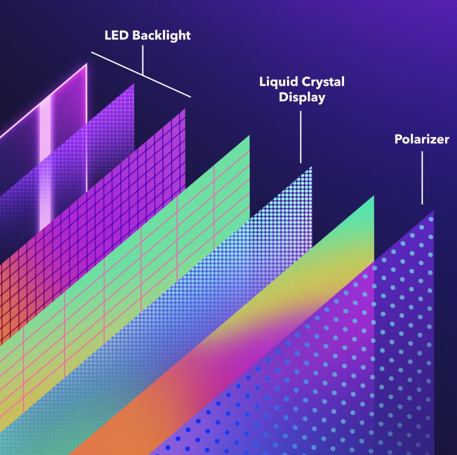
Self-emissive pixels independently control color, with DCI-P3 gamut coverage of 98% (LCD approx. 72%), and QDOLED exceeding 100% (e.g., Sony A95L reaching 99% DCI-P3, ΔE<1).

Durability
Laser encapsulation water vapor transmission rate (WVTR) <10⁻⁶ g/m²/day, with the surface covered by UTG/CPI protective layers.
iPhone 15 Pro Max OLED screen 1.5m drop integrity rate is 95%, with a lifespan >100,000 hours (brightness decay <20%).
Flexible Substrates
The mainstream flexible substrate uses Polyimide (PI), with a thickness typically between 10-20μm.
The material must possess heat resistance of $T_g$ > 450°C to match the LTPS process, and the Coefficient of Thermal Expansion (CTE) must be controlled within 10 ppm/°C.
Through Laser Lift-Off (LLO) technology, the carrier glass with a thickness of approx.
0.5mm can be removed, allowing the display module to achieve an ultimate folding radius of R < 1mm.
Substrate Materials
PI
-
Thermal Stability: The LTPS process requires multiple annealing steps between 420°C and 450°C. Ordinary polymers soften at 250°C, while specialized display-grade PI, by introducing aromatic ring structures, raises its glass transition temperature ($T_g$) to above 450°C.
-
Coefficient of Thermal Expansion (CTE): Any difference in expansion coefficients between the substrate and the inorganic films deposited above (e.g., $SiN_x$) will lead to film cracking after cooling. Industrial standards require PI's CTE to be between 3 ppm/°C and 10 ppm/°C to match the expansion rates of silicon powder or metal traces.
-
Thickness Control: The dry film thickness after liquid PI coating is usually set at 10μm to 15μm. Every 1μm increase in thickness fluctuation leads to uneven laser energy absorption during the stripping process.
CPI
Ordinary PI appears deep yellow due to the presence of intra-molecular Charge Transfer Complexes (CTC), making it unsuitable for cover plates where light must pass through.
CPI (Colorless Polyimide) breaks this limitation by introducing fluorine atoms or alicyclic structures.
-
Transmittance and Haze: CPI has an average light transmittance of over 90% in the 380nm - 780nm band, with Haze below 1%. This ensures accurate reproduction of display colors and avoids color shifting.
-
Modulus and Hardness: Compared to ordinary PI, CPI's Young's modulus ranges from 3 GPa to 5 GPa. When used as a cover plate, a high-hardness coating (HC) layer of about 5μm is typically applied to the surface to reach a pencil hardness of 3H - 5H, compensating for the polymer's susceptibility to scratching.
-
Weather Resistance: CPI must pass a 1000-hour "Double 85" test (85°C temperature, 85% humidity) to ensure the change in Yellow Index (YI) is $\Delta YI < 0.5$.
Ultra-Thin Glass (UTG)
-
Geometric Dimensions: Thinned glass thickness drops to 30μm. At this thickness, the internal stress distribution of the glass changes, allowing the bending radius $R$ to reach below 1.5mm.
-
Chemical Strengthening (Slimming & Strengthening): Glass undergoes ion exchange in a potassium nitrate (KNO3) molten salt bath. Larger potassium ions replace sodium ions on the glass surface, creating a Compressive Stress (CS) layer of 400 MPa to 800 MPa, with the Depth of Layer (DoL) typically controlled around 10μm. This stress layer effectively offsets the tensile stress generated during bending, preventing the glass from shattering.
-
Optical Consistency: UTG has a refractive index of approx. 1.5 and possesses extremely high surface flatness (roughness $Ra < 0.5nm$), eliminating subtle visual ripples that may appear on polymer substrates.
| Detailed Metric Comparison | Standard PI | High-Performance CPI | Strengthened UTG |
|---|---|---|---|
| Young's Modulus | 4.5 GPa | 3.2 GPa | 72 GPa |
| Refractive Index | 1.6 - 1.7 | 1.5 - 1.55 | 1.51 |
| WVTR (g/m²/day) | $10^0$ | $10^0$ | $10^{-6}$ (Intrinsic) |
| Surface Hardness (Uncoated) | < 1H | < 1H | 9H (Mohs 5-6) |
| Elongation at Break | 10% - 20% | 15% - 25% | < 1% |
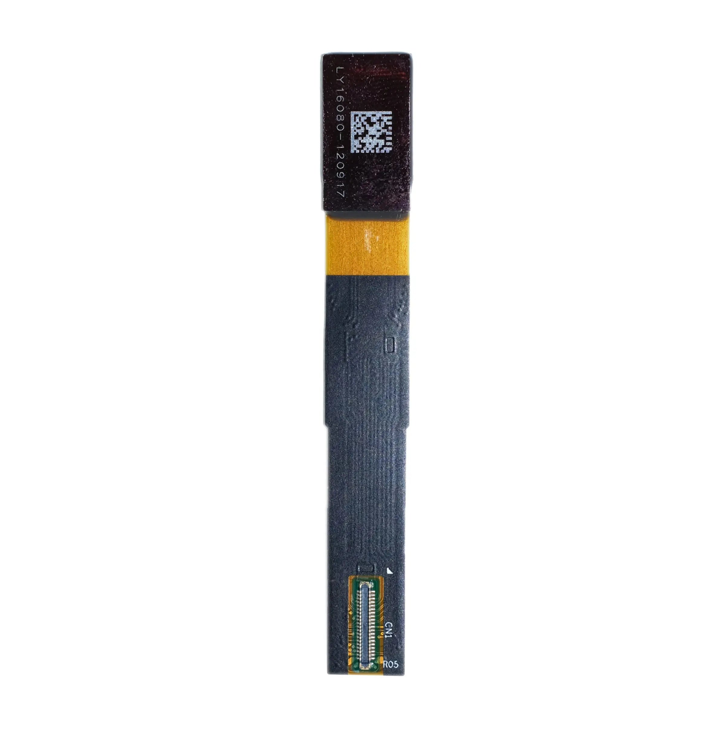
Stripping Process
Laser Energy
An excimer laser with a common wavelength of 308nm is used.
The laser penetrates the carrier glass, generating energy of approx. 200mJ/cm² at the PI surface.
If the PI absorption rate is insufficient, the laser will penetrate the substrate and damage the driving circuits above.
Residual Stress
After stripping, the PI film will shrink due to the release of internal stress.
The adhesion between the high-density metal wiring layer and the substrate must be greater than 5N/cm;
otherwise, interlayer delamination will occur at the moment of stripping.
Bending Limits
Metal Traces
Metal traces on flexible substrates (usually aluminum, copper, or Mo-Al-Mo structures) serve as channels for electrical signal transmission.
Micro-crack expansion during bending is the primary cause of screen failure (black screen).
-
Geometric Design: Traces no longer use straight designs but adopt Zig-zag or nano-grid structures. These structures absorb stress through geometric deformation rather than lattice stretching when bent.
-
Resistance Change Rate Monitoring: Experimental data shows that when trace width is reduced from 5μm to 2μm, the fatigue life of the material increases. After 100,000 continuous bends, the overall impedance fluctuation must stay within ±2%.
-
Grain Size Control: During metal deposition, metal grain size is controlled by adjusting sputtering power and substrate temperature. A fine grain structure can effectively block the linear expansion path of cracks.
OCA/OCR
In multi-layer structures, Optical Clear Adhesive (OCA) between layers acts to buffer and release shear stress.
-
Storage Modulus: At room temperature, the storage modulus of OCA is typically maintained between 50 kPa and 100 kPa. A modulus that is too high leads to excessive bending torque, increasing the risk of peeling; a modulus that is too low cannot provide sufficient structural support when folded.
-
Rheological Behavior: When the screen is in a static fold (e.g., a phone folded overnight), OCA undergoes creep. The material is required to remain shape-stable at 60°C, and after unfolding, the thickness recovery rate must reach over 99.5% within one minute.
-
Peel Strength: The peeling force between the substrate and functional layers must be constant above 8N/25mm to counter the outward thrust generated during folding.
Environmental Temperature and Humidity
-
Low-Temperature Brittleness: At extreme low temperatures of -20°C, the modulus of PI substrates and OCA will rise 3-5 times. At this point, the material transitions from a high-elastic state to a glassy state, and the original bending radius $R=1.5mm$ might trigger microscopic fractures.
-
High-Temperature Softening: At 85°C, adhesive softening may lead to slippage (Slip) between layers, resulting in permanent visual ripples in the crease area.
-
Water Vapor Permeation Path: During bending, the TFE encapsulation layer may develop nano-scale cracks invisible to the naked eye. Experimental data shows that after frequent bending, the WVTR will drop from an initial $10^{-6} g/m^2/day$ to $10^{-4} g/m^2/day$, which determines the module's effective working life.
Different forms of flexible screens challenge physical limits in different dimensions:
| Morphology Type | Typical Radius ($R$) | Mechanical Challenge |
|---|---|---|
| In-folding Screen | 1.0mm - 3.0mm | Extremely high compressive stress, prone to film wrinkling (Buckling) |
| Out-folding Screen | 4.0mm - 6.0mm | Continuous tensile stress, extremely high cover plate hardness requirement |
| Rollable Screen | 10mm - 15mm | Dynamic cumulative stress, requires solving sliding friction and wear |
| Stretchable Screen | Irregular | Strain balance within a 2D plane, requires elastic backing |
Bending performance depends on the positioning of the Neutral Solvent Plane.
As the bending radius $R$ shrinks from 5mm to 1mm, edge tensile stress grows exponentially.
By controlling the total module thickness between 100μm - 150μm and adjusting the Young's modulus of each layer, the Thin Film Transistor (TFT) can be placed on the neutral plane where stress is zero.
Current industrial standards require passing 200,000 dynamic bending tests within the -20°C to 60°C range, with the metal trace resistance change rate below 5%.
Color Gamut
The OLED color gamut is determined by the triangular area defined by RGB primary colors in the CIE 1931 coordinate system.
Mainstream modules currently use light-emitting materials with a Full Width at Half Maximum (FWHM) of under 30nm to achieve 100% DCI-P3 coverage.
The red coordinate is typically located at $(0.680, 0.320)$ and the green at $(0.265, 0.690)$.
By adjusting the microcavity optical thickness, monochromatic purity can be improved by over 15%, bringing the gamut area to 110% of the NTSC standard, providing accurate mapping for over 1.07 billion colors in HDR10+ video streams.
Standard Comparison
sRGB and Rec.709
The sRGB standard was jointly established by Microsoft and HP in 1996, primarily applied to PC monitors and internet images.
Rec.709 is the industry standard for High-Definition Television (HDTV).
The color gamut coverage of both is identical, though they differ slightly in Gamma values (usually 2.2 or 2.4) and white point settings.
-
Coordinate Definitions:
- Red: $(0.640, 0.330)$
- Green: $(0.300, 0.600)$
- Blue: $(0.150, 0.060)$
-
OLED Adaptation Logic:
Since OLED's native gamut far exceeds sRGB, the Display Driver IC (DDIC) must perform gamut mapping/reduction algorithms when displaying such content. Without intervention, the native wide gamut would overstretch an orange coordinate of $(0.50, 0.40)$ in sRGB to a pure red region near $(0.60, 0.35)$, resulting in unnaturally reddish skin tones. -
Quantitative Metric:
A qualified mobile OLED module should maintain color accuracy in sRGB mode at Average $\Delta E < 1.2$.
DCI-P3
DCI-P3 is the color space defined by the Digital Cinema Initiatives alliance.
It features a broader range of reds and greens than sRGB, particularly with deeper greens in the 520nm to 550nm band.
-
Technical Parameters:
- Compared to sRGB, DCI-P3 moves the green coordinate about 15% Euclidean distance toward the spectral edge.
- Its red coordinate moves from $(0.64, 0.33)$ to $(0.68, 0.32)$, requiring OLED materials with higher monochromatic purity.
-
Hardware Implementation:
To cover 100% DCI-P3, the OLED Emission Layer (EML) typically uses Phosphorescent materials. Red phosphorescent materials have a quantum efficiency near 100%, providing sufficient saturation. During module fabrication, anode reflectivity is adjusted (usually set above 90%) to enhance the microcavity effect, stabilizing DCI-P3 coverage. -
Ambient Contrast Ratio (ACR):
In DCI-P3 mode, OLED contrast is usually marked at 1,000,000:1. At 1000 nits peak brightness, the coordinate shift of dark colors must be controlled within JNCD < 0.5.
Rec.2020
Rec.2020 is the standard set by the International Telecommunication Union (ITU) for Ultra-High-Definition Television (UHDTV).
-
Coordinate Extremes:
- Red: $(0.708, 0.292)$
- Green: $(0.170, 0.797)$
- Blue: $(0.131, 0.046)$
-
Technical Challenge Data:
The green vertex of Rec.2020 lies almost at the edge of the CIE 1931 curve. Current top-tier mobile OLED modules typically achieve coverage between 76% and 83%. To achieve over 90% coverage, the FWHM of RGB primary colors must be compressed to 20nm or lower. -
Material Science Bottleneck:
To reach Rec.2020 red coordinates, the material molecular structure must be extremely regular, which often comes with a decrease in thermal stability. The industry currently uses Tandem stacking to lower the driving brightness of each layer, thereby gaining color purity.
NTSC
While the NTSC gamut (1953 version) is no longer a standard for content production in the digital age, it is still frequently used as a quantitative percentage reference for screen quality.
-
Conversion Ratios:
- 100% sRGB is approx. 72% NTSC.
- 100% DCI-P3 is approx. 96% NTSC.
- 100% Adobe RGB is approx. 95% NTSC.
-
Quantitative Meaning:
If an OLED module claims 110% NTSC gamut, its color space volume is massive, but without a high-precision 3D LUT (Look-Up Table), the images viewed by the user will be severely distorted.
Adobe RGB
Adobe RGB is wider in the cyan-green section than sRGB, primarily to cover the CMYK printing gamut.
-
Distinguishing Details:
- Adobe RGB coordinates: Red $(0.64, 0.33)$, Green $(0.21, 0.71)$, Blue $(0.15, 0.06)$.
- Compared to DCI-P3, Adobe RGB emphasizes the extension of Cyan-green, while DCI-P3 emphasizes the fullness of Golden-yellow and Red.
-
OLED Application:
In professional drawing tablets or high-end laptops, an Adobe RGB mode is often provided. This requires the DDIC to support 12-bit internal computing precision to prevent color Banding during gamut conversion.
OLED modules are designed to define the absolute positions of RGB triangular vertices via the CIE 1931 coordinate system.
The green coordinate defined by the sRGB standard is $(0.300, 0.600)$, while DCI-P3 extends it to $(0.265, 0.690)$, increasing the color space volume by approx. 26%.
The Rec.2020 standard pushes the red vertex to the spectral limit of red light at $(0.708, 0.292)$, covering 75.8% of visible colors in nature.
Through 10-bit depth driving, OLED can achieve 1.024 billion grayscale levels under these standards, ensuring an analytical precision of $\Delta E < 2$ during gamut switching.
Accuracy Influences
Evaporation Process
OLED color generation relies on depositing organic materials through a Fine Metal Mask (FMM) onto the backplane in a vacuum.
-
Color Mixing: If the FMM displacement after thermal expansion exceeds 2-5 microns, RGB materials will deposit into the wrong pixel areas. Even 0.5% material overlap can cause a shift in the primary color coordinates. For example, green material mixing into red pixels shifts the red coordinate from $(0.68, 0.32)$ toward $(0.60, 0.40)$.
-
Aperture Ratio: The ratio of effective light-emitting area to total area. As pixel density (PPI) rises above 500, the aperture ratio typically drops to 15%-20%. Smaller apertures require higher current density per unit area to maintain brightness, which exacerbates the Stark effect in organic materials, leading to spectral broadening and reduced color purity.
TFT
-
Mobility Uniformity: Low-Temperature Polycrystalline Silicon (LTPS) backplanes produce non-uniform grains during laser annealing. If grain size distribution is uneven, current deviation under the same driving voltage can reach 10%-15%. This current fluctuation appears visually as "Mura" or inaccurate grayscale.
-
IR Drop Compensation: In large-sized modules, current flowing through power lines causes a voltage drop. Without internal compensation (e.g., using 7T1C pixel circuits), pixels near the power input will be brighter and deeper in color than those further away. High-precision modules require full-screen IR drop fluctuation controlled within 50mV to ensure color uniformity exceeds 95%.
FWHM
-
Doping Concentration: In the Emission Layer (EML), the Dopant ratio is typically between 0.5% and 3.0%. Increasing concentration causes quenching effects, leading to spectral redshift and broadening; too low a concentration results in insufficient energy transfer. Precise control of doping fluctuations within ±0.1% is the prerequisite for stable batch-to-batch color accuracy.
-
Triplet Exciton Management: Phosphorescent materials use triplet excitons for light, and their spectra are usually wider than fluorescent materials. To achieve high accuracy under the P3 gamut, the design introduces Prime Layers to restrict exciton diffusion, compressing FWHM to 30nm (red) and 25nm (green).
VAD (Viewing Angle Dependency)
-
Blue Shift: In microcavity interference, the optical path length shortens as the viewing angle θ increases (following the $L\cos\theta$ relationship). When the angle increases from 0 to 60 degrees, the center wavelength may shift by more than 15nm.
-
Refractive Index Matching of Cover Glass and Polarizer: During module lamination, the refractive index of OCA (typically 1.48-1.52) must be highly matched with the polarizer and OLED encapsulation layer. Refractive index jumps cause multiple reflections at interfaces, producing a Rainbow effect that interferes with true color representation.
CMS (Color Management System)
-
3D LUT Precision: High-end modules use 17x17x17 or higher node Look-Up Tables. With 17 calibration points on each of the R, G, and B axes, non-linear color bias is corrected via interpolation algorithms. If node count is insufficient (e.g., only 5x5x5), obvious color Banding will appear in gradients like a sunset sky.
-
Gamma Curve Alignment: The standard Gamma is 2.2. In OLED, due to leakage current at low grayscales, Gamma near the black field is extremely difficult to control. Modules require 10-bit or 12-bit digital driving to perform multi-point independent adjustment in the 0.1 to 5 nits low-brightness range to prevent dark detail loss or color tinting.
When brightness rises from 100 nits to 1000 nits (HDR mode), sub-pixel temperature rise causes changes in the bandgap width, affecting the emission wavelength.
High-performance modules require primary color coordinate drift to be less than 0.002 under high-brightness pulses.
In bright environments, reflected light on the screen surface washes out colors.
By introducing a Circular Polarizer, reflectivity can be reduced below 4%, maintaining over 80% of the original gamut volume under high light.
Durability
OLED durability is determined by Water/Oxygen Barrier Rate ($10^{-6} g/m^2/day$), LT90 lifespan (time to 10% brightness decay), and mechanical fatigue strength.
By using multidentate phosphorescent materials and Tandem structures, module current density can be reduced by 30%, increasing typical working life to over 50,000 hours.
In flexible scenarios, neutral plane shifting technology ensures that at a bending radius of $R=1.0mm$, the strain on ITO electrodes remains below 0.1%.
Environmental Barrier
Thin Film Encapsulation (TFE)
-
Inorganic Layers: Usually Silicon Nitride ($SiN_x$) prepared by PECVD or Aluminum Oxide ($Al_2O_3$) prepared by ALD.
- $SiN_x$ Density: Deposition density must reach over 2.4g/$cm^3$ to provide sufficient lattice density.
- Stress Control: Internal stress of inorganic films must be controlled between -200MPa and 200MPa to prevent cracking during bending.
- Thickness: The first inorganic layer is usually set at 0.8μm - 1.2μm to establish the first physical barrier.
-
Organic Planarization Layers: Acrylic or epoxy resins applied via IJP (Inkjet Printing).
- Particle Coverage: Tiny dust particles (0.5μm) in production cause growth defects in inorganic layers. The organic layer fills gaps around these particles through liquid flow, with a thickness of approx. 5μm - 8μm.
- Decoupling Effect: The organic layer cuts off the vertical propagation path of defects between two inorganic layers, forcing water/oxygen molecules to diffuse laterally for several millimeters to find the next defect, greatly extending permeation time.
Edge Sealing
-
Dam & Fill Structure: Two photoresist ridges (Dams) are set around the display area to restrict the flow of the printed organic liquid.
-
Seal Width: Modern narrow-bezel designs require seal width to shrink from 1.0mm to 0.3mm - 0.5mm.
-
Lagrangian Permeation Model: Calculated by Fick's Second Law, the permeation path length has a square relationship with effective life. To compensate for life loss due to bezel shrinkage, step coverage of inorganic films at the encapsulation edge must be improved, ensuring sidewall thickness is not less than 60% of the top surface thickness.
ALD (Atomic Layer Deposition)
To pursue longer lifespans (e.g., 15 years for automotive displays), ALD is largely replacing or assisting PECVD.
-
Self-limiting Reaction: ALD uses precursor gases (e.g., TMA) for atomic layer growth on the substrate, filling 10nm micro-pores.
-
Barrier Improvement: At the same thickness, $Al_2O_3$ formed by ALD has 10 - 50 times the barrier performance of PECVD $SiN_x$.
-
Hybrid Encapsulation: A common quantitative combination is 1 layer ALD + 1 layer PECVD, reducing total thickness by 40% while achieving a WVTR in the magnitude of $10^{-7} g/m^2/day$.
Desiccants and Adsorbents
In rigid OLEDs or specific modules, chemical Getters are integrated into the internal space.
-
Material Composition: Mostly nano-scale Barium Oxide (BaO) or Calcium Oxide (CaO) particles dispersed in specialized polymer matrices.
-
Adsorption Capacity: High-quality getters must absorb over 100mg of water per gram.
-
Thickness: Desiccant patches are usually 20μm - 50μm thick, laminated between the backplane and encapsulation cover to trap residual moisture that penetrates the first barrier.
OLED encapsulation must achieve a WVTR below $10^{-6} g/m^2/day$, six orders of magnitude higher than LCD.
Current mainstream uses the TFE structure, where two 500nm - 1000nm inorganic layers (e.g., $SiN_x$) sandwich one 5μm - 10μm organic layer.
This design blocks over 99.9% of permeation paths, maintaining brightness stability for organic materials for 15,000 to 30,000 hours in standard environments, preventing pixel oxidation (black spots).
Material Anti-Aging
Organic Emissive Materials
The OLED emissive layer consists of Host and Dopant materials.
Aging is primarily due to chemical bond breakage of Excitons in high-energy states.
-
Bond Energy Analysis: The $C-H$ bond energy in blue fluorescent materials is approx. 4.3 eV, while blue excitons have energies of 2.7 eV - 3.0 eV. Local accumulation of excitons leads to energy superposition and bond breakage, creating radical fragments that act as non-radiative centers, consuming electrons without producing photons.
-
Triplet-Polaron Quenching (TPQ): At high current densities (over 100 mA/$cm^2$), excitons collide with charge carriers. Data shows TPQ contributes over 40% of initial brightness decay.
-
Triplet-Triplet Annihilation (TTA): Under high brightness, triplet exciton concentration rises, and collisions lead to energy loss and heat. Optimizing doping ratios (usually 3% - 8%) can increase exciton diffusion length and reduce collision probability.
Deuteriation
-
C-D Bond Advantage: Deuterium is twice as heavy as hydrogen, so $C-D$ bonds have lower vibration frequencies and smaller zero-point energy, making them harder to break by high-energy excitons than $C-H$ bonds.
-
Lifespan Comparison:
- Non-deuterated blue material: LT95 is approx. 200 hours at 3000 nits.
- Fully-deuterated blue material: LT95 extends to over 1000 hours at the same brightness, a 400% increase.
-
Efficiency Maintenance: Deuteration does not change the energy level structure (HOMO/LUMO), so External Quantum Efficiency (EQE) stays stable at 20% - 25% while extending life.
Tandem
Tandem structures vertically connect multiple emissive Units via Charge Generation Layers (CGL), physically distributing the material stress.
-
Current Density Reduction: To reach the same brightness (e.g., 2000 nits), the driving current for a 2-Unit tandem is only 50% of a single-layer structure.
-
Thermal Load Reduction: Per Joule's Law ($P = I^2R$), halving the current reduces heat to 25% theoretically. Lower operating temperatures effectively inhibit recrystallization of organic materials.
-
Lifespan Multiplier: Experiments show LT80 (20% decay) for tandem structures is 3.5 - 4 times that of single layers. This is now standard for automotive displays (requiring 15-year life) and high-end tablets.
Transport Layer Materials
Beyond the emissive layer, the heat resistance of HTL and ETL determines performance under high-temperature conditions.
-
Glass Transition Temperature ($T_g$): If ambient temperature approaches $T_g$, the organic film transitions to a rubbery state, causing molecular disorder.
- Standard materials: $T_g$ approx. 85°C - 95°C.
- High-reliability materials: $T_g$ must exceed 120°C to ensure no phase separation during 95°C storage tests.
-
Hole Blocking Layer (HBL): Using materials with deep HOMO levels (approx. -6.5 eV) prevents holes from penetrating into the ETL, reducing unintended interface aging reactions.
Pixel Driving Compensation
Hardware material improvements are assisted by software compensation to extend perceived life.
-
Current Compensation: The driver IC records cumulative on-time and current intensity for each sub-pixel.
-
Algorithm Logic: When the system predicts a 2% physical decay in a blue sub-pixel, the circuit automatically raises the bias voltage by approx. 10mV - 50mV to increase current injection, restoring brightness to the initial state.
-
Optical Sensor Closed-Loop: Some high-reliability modules integrate photosensitive elements at the bezel to monitor RGB intensities in real-time, keeping color temperature deviation ($\Delta CCX/CCY$) within 0.003.
Auxiliary Materials
-
Polarizer Filtering: UV radiation is a major cause of outdoor aging. Polarizers must integrate a UV cut-off layer, with a blocking rate above 99% for bands below 380nm.
-
Low-Acid OCA: Residual free acid in adhesives can corrode ITO or penetrate encapsulation. Durable modules require OCA acid value to be less than 0.01 mg KOH/g.
-
Cathode CPL: Depositing a high-refractive-index Capping Layer (CPL) above the cathode not only improves brightness via interference but also acts as an extra physical barrier against cathode oxidation.
OLED anti-aging is achieved through Deuteration (lifespan up 2-5 times) and Tandem structures (current load down 50%).
High-performance blue phosphorescent LT95 has now exceeded 20,000 hours at 1000 nits.
By introducing high $T_g$ ($> 110°C$) HTL materials and TADF technology, exciton quenching can be reduced by 15%, maintaining color coordinates within $\Delta u'v' < 0.002$ in high-heat environments.
Mechanical Endurance
Flexible Bending Stress
Flexible OLED modules consist of over ten thin-film layers including covers, polarizers, touch layers, emissive layers, and substrates.
Each has a different Young's Modulus, creating complex internal stresses when bent.
-
Neutral Plane Shifting Technology: By precisely calculating layer thicknesses and elastic moduli, designers place fragile layers like TFE and ITO electrodes near the "neutral plane."
- On the neutral plane, tensile and compressive stresses cancel out, making the resultant force approach 0.
- Data shows that at a 1.5mm radius, an offset of over 10μm from the neutral plane increases ITO cracking risk by 60%.
-
OCA Shear Force: Using OCA with high creep performance (thickness 25μm - 50μm) allows for micro-displacements between functional layers during bending, releasing accumulated shear stress.
UTG and CPI
-
Ultra-Thin Glass (UTG): Thinned to 30μm via chemical strengthening.
- Endurance: Can withstand over 200,000 bends, with crease depth usually controlled within 0.1mm.
- Hardness: Reaches 6H - 7H, effectively resisting scratches from daily objects like coins or keys.
-
Colorless Polyimide (CPI): Approx. 40μm - 80μm thick with extremely high impact toughness. While hardness is lower than glass (approx. 2H - 3H), it performs better in low temperatures (e.g., -20°C) without brittle fracture.
Module Heat Dissipation
OLEDs are current-driven and generate significant heat at high brightness.
Heat accumulation leads to fast aging and adhesive failure.
-
High Thermal Conductivity Backplanes: Synthetic graphite sheets (horizontal conductivity 1500 W/m·K) are laminated below the substrate. Trace copper foil layers (10μm) uniformize the temperature at the Driver IC (D-IC) from 55°C, keeping the overall delta within 3°C.
-
CTE Matching: CTE of different layers must match. If the difference between the PI substrate (12 - 15 ppm/°C) and inorganic encapsulation layers exceeds 10 units, thermal shock testing will cause interlayer delamination and encapsulation failure.
Impact Resistance
-
Buffer Support Layers: PF or PU foam (0.1mm - 0.2mm) at the module base undergoes plastic deformation during impact, absorbing over 70% of the energy to protect thin-film circuits.
-
Pen Drop Test: Simulating stylus pressure, the screen must withstand 200g - 500g of pressure for 100,000 continuous clicks at the same position without pixel abnormality.
Verification Standards
| Test Name | Metric | Pass Criteria |
|---|---|---|
| Dynamic Bending | R=1.5mm, 200k cycles | Impedance change < 10%, no visible crease |
| Ball Pressure | D=10mm, 20N load | No flickering, no polarizer denting |
| Torsion Test | ±10° angle, 5k cycles | No edge delamination, normal signals |
| Drop Test | 1.2m height, 6 sides 4 corners | No cover breakage, full functionality |
Mechanical endurance also includes material behavior at non-standard temperatures.
High-Temperature Storage: 500 hours at 95°C.
Requires no bubbles in OCA and film shrinkage under 0.1%.
Low-Temperature Dynamic Test: Bending at -20°C.
Monitors for micro-cracks in TFE layers as materials become brittle.
Optimized composite structures can increase critical crack strain from 0.5% to 0.8% in the cold.
Read more
OLED is based on self-emissive organic pixels (light up when energized, turn off when power is cut), with independent pixel light control. It emits no light at all when turned off, reaching a contr...
OLED achieves infinite contrast (>100,000:1) and refresh rates exceeding 120Hz thanks to its self-emissive characteristics, making it suitable for dynamic video; Electronic paper (ePaper) relies...
Leave a comment
This site is protected by hCaptcha and the hCaptcha Privacy Policy and Terms of Service apply.