


The Guide to Micro OLED | Technology, Features & AR/VR Applications
Micro OLED is a silicon-based OLED technology with a pixel density exceeding 3000 PPI and a brightness of several thousand nits.
It is small in size, has low power consumption, and offers extremely fast response times, completely eliminating the "screen door effect" in AR/VR.
It is a key core technology for achieving ultra-high-definition immersive experiences in high-end head-mounted displays and possesses extremely high professional value.
Technology
Micro OLED utilizes 12-inch CMOS silicon wafers as the circuit control foundation, shrinking pixel pitch to between 4 and 9 micrometers.
Within a 0.7-inch area, it can integrate over 7 million sub-pixels, achieving a PPI of over 3500.
Compared to traditional display technologies, its electron mobility is more than 100 times higher.
Through a 2- to 3-layer W-OLED tandem structure, the panel provides 3000 to 5000 nits of brightness while maintaining power consumption under 500 milliwatts and a response time of less than 10 microseconds.
Silicon Wafer Circuit Backplane
Micro OLED abandons traditional glass or plastic substrates in favor of 300 mm (12-inch) monocrystalline silicon wafers as the electrical foundation.
This material shift allows the display backplane to leap from low-performance Thin-Film Transistors (TFT) to high-performance Complementary Metal-Oxide-Semiconductor (CMOS) processes.
The electron mobility of monocrystalline silicon is typically between 500 and 700 cm²/Vs, whereas Low-Temperature Polycrystalline Silicon (LTPS), commonly used in high-end smartphone screens, is only 50 to 100 cm²/Vs.
This order-of-magnitude difference allows complex and refined circuit modules to be placed within extremely small spaces.
In a standard 0.7-inch display module, the silicon-based backplane can carry hundreds of millions of transistors, fully integrating logic control, digital-to-analog conversion, and pixel lighting control into a single chip.
This high degree of physical integration eliminates a large number of interconnect pins between the external driver chip and the display panel, significantly reducing electromagnetic interference and energy loss during signal transmission.
Regarding semiconductor process nodes, Micro OLED backplanes typically utilize mature processes ranging from 28 nm to 65 nm.
Taking the 28 nm process as an example, it can construct complete pixel control units within a physical width of less than 1 micrometer.
Due to the extremely high precision of the CMOS process, pixel pitch has been pushed to the limit of 4 to 9 micrometers.
In the same display area, the number of pixels placed on a silicon-based backplane is more than 10 times that of a traditional glass substrate.
Each pixel unit is not just a simple switch but contains a current compensation circuit composed of 5 to 7 transistors.
This complex unit circuit design is intended to resolve voltage threshold differences within extremely small areas of the monocrystalline silicon surface, ensuring that millions of pixels maintain high consistency even under low current states.
To support 4K resolution and refresh rates from 90Hz to 120Hz, high-speed data interfaces such as MIPI (Mobile Industry Processor Interface) or eDP (Embedded DisplayPort) are integrated into the backplane, with data throughput reaching dozens of Gbps per second.
The backplane integrates multi-channel 10-bit or 12-bit Digital-to-Analog Converters (DACs), converting received digital image information into precise voltage signals.
To achieve more delicate grayscale performance, hierarchical voltage control is introduced into the circuit design.
In high-brightness mode, the circuit can provide 4V to 10V operating voltage to activate the OLED emitting layer, while the logic control section maintains a low voltage of 0.9V to 1.2V. This dual-voltage domain architecture balances display brightness and circuit power consumption.
To meet the strict contrast requirements of near-eye displays, Pulse Width Modulation (PWM) technology is utilized at the circuit level.
This method adjusts brightness by controlling the proportion of light-emitting time within a single frame period, rather than relying solely on current magnitude. The application of PWM effectively avoids color shifts in OLED materials under low current, allowing the screen to present deep blacks and accurate colors even in extremely dark scenes.
Since OLED emitting materials require surface flatness at the nanometer level, the wafer must undergo Chemical Mechanical Polishing (CMP) after circuit processing.
The surface roughness (Ra) after polishing is controlled to within 0.5 nanometers.
If tiny ripples exist on the surface, it will lead to uneven thickness of the deposited organic emitting layer, resulting in electric field strength differences and color drift.
To improve light utilization efficiency, high-reflectivity metals such as Aluminum (Al) or Silver (Ag) are deposited on the top layer of the pixel circuit as reflective anodes.
This metal layer not only serves as a conductor but also reflects back-emitted light from the OLED toward the observer.
The entire backplane exhibits excellent thermal conductivity; silicon's heat dissipation efficiency is far higher than glass, allowing temperature rises from high-brightness operation to be quickly exported to the module casing, extending the physical lifespan of the organic materials.
| Technical Parameter | Specification Detail | Physical Implementation |
|---|---|---|
| Wafer Size | 300 mm (12-inch) | Industrial-grade monocrystalline silicon production line |
| Logic Process Node | 28 nm / 40 nm / 55 nm | CMOS lithography and doping process |
| Electron Mobility | Approx. 600 cm²/Vs | Monocrystalline silicon lattice structure |
| Pixel Circuit Density | Approx. 20,000 units/mm² | Nanometer-scale metal routing technology |
| DAC Precision | 10-bit to 12-bit DAC | In-situ integrated signal processing circuitry |
| Surface Flatness | < 0.5 nm (Ra) | Multi-stage CMP polishing process |
| Static Power Consumption | < 50 mW | Low-power CMOS leakage current control |
A temperature compensation algorithm module is typically integrated within the backplane to monitor temperature rises across different areas of the wafer in real-time and automatically adjust current output, preventing brightness non-uniformity caused by thermal runaway.
For AR scenarios, local dimming functionality is added to the circuit design, allowing power to be supplied only to areas where images are displayed, while other areas remain in a zero-power state.
This power-on-demand logic allows Micro OLED to maintain high brightness over 3000 nits while keeping overall power consumption at levels comparable to smartphone screens.
By building micro-lens control logic directly onto the silicon, the backplane can even support early-stage eye-tracking data pre-processing, reducing the computational pressure on the main processor.
Three-Unit Tandem Emitting Structure
The total thickness of the light-emitting layer is typically controlled between 200 nm and 500 nm, containing over 25 thin-film layers with various functions.
In a 3-Unit architecture, three independent light-emitting centers are electrically connected via Charge Generation Layers (CGL).
This multi-layer tandem approach effectively mitigates the decay rate of organic materials under high brightness, allowing the module's T50 lifespan (the time for brightness to decay to half) to exceed 30,000 hours even at 5000 nits of output.
The internal construction of each emitting unit consists of a Hole Injection Layer (HIL), Hole Transport Layer (HTL), Emitting Layer (EML) with Red/Green/Blue dopants, Electron Transport Layer (ETL), and Electron Injection Layer (EIL).
The thickness of the HIL is precisely controlled between 5 nm and 15 nm, and its work function must highly match the underlying metal anode.
The HTL consists of high-mobility small-molecule materials with a thickness distribution of 40 nm to 100 nm, used to adjust the physical position of the emitting center within the microcavity.
The Emitting Layer (EML) is where energy conversion occurs, usually combining phosphorescent yellow or green materials with fluorescent blue materials.
This "white light" scheme produces a wide spectral output covering most of the CIE 1931 color space.
To achieve a pure white point (D65), the doping concentration deviation of each layer must be controlled within 0.1%.
The Charge Generation Layer (CGL) is located between two emitting units and serves as the electrical hub that enables the tandem structure to function. It consists of a p-n junction formed by an n-type doped layer and a p-type doped layer.
When an external bias is applied, the CGL generates electrons and holes at its interface, injecting them in opposite directions into adjacent emitting units.
This internal charge injection mechanism makes the overall driving voltage the algebraic sum of the voltages of each layer, with a typical operating voltage range between 10V and 18V.
By optimizing CGL energy level alignment, charge injection efficiency can reach nearly 100%, ensuring high conversion efficiency from electrical energy to light.
This layer is only about 10 nm thick but must possess extremely high light transmittance to prevent unnecessary absorption loss.
| Physical Parameter | 2-Unit Tandem Spec | 3-Unit Tandem Spec |
|---|---|---|
| Total Organic Layer Thickness | 250 - 350 nm | 400 - 550 nm |
| Drive Current Density | 50 mA/cm² | 35 mA/cm² (at same brightness) |
| Luminous Efficiency | 60 - 80 cd/A | 100 - 130 cd/A |
| Startup Voltage | 7V - 9V | 11V - 14V |
| Color Saturation (DCI-P3) | Approx. 95% | Over 98% |
| Peak Brightness | 3000 nits | 6000 - 10000 nits |
Before light leaves the organic stack, it experiences enhancement from the Microcavity Effect.
The silicon-based aluminum anode at the back acts as a total reflection mirror, while the thin-film cathode at the top acts as a semi-transparent mirror.
The optical distance between the two reflective surfaces must match an integer multiple of a specific wavelength.
By fine-tuning the nanometer-scale thickness of the HTL, the peaks of the red, green, and blue light can be locked to the resonance wavelengths of the microcavity.
This optical interference phenomenon can compress spectral bandwidth from 50 nm to about 20 nm, greatly improving color purity.
This effect results in highly directional emission, with a luminous intensity in the normal direction 2 to 3 times higher than conventional scattered light.
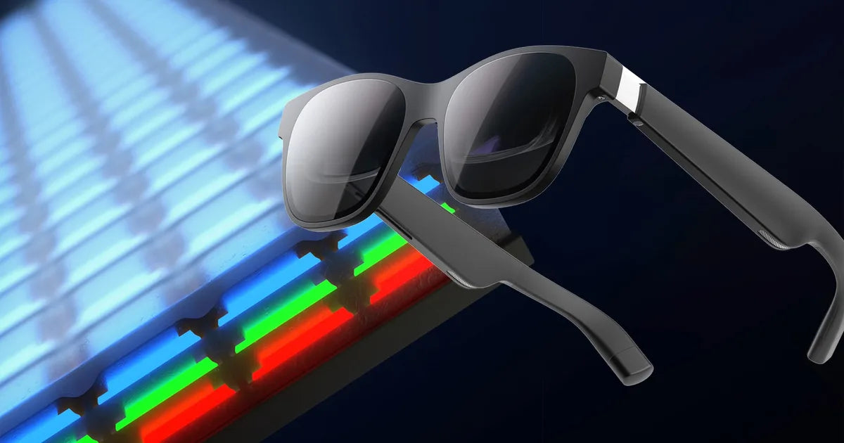
To convert white light into visible color images, a highly precise optical Color Filter (CF) is placed above the top encapsulation layer.
Each color filter unit is typically only 2 micrometers by 6 micrometers. These filters are made of high-performance photosensitive resin materials with a thickness under 1 micrometer.
Due to the extremely small sub-pixel size, filter manufacturing utilizes semiconductor-level lithography processes rather than traditional printing processes.
To reduce light interference (crosstalk) between different pixels, Black Matrix (BM) material is filled between the red, green, and blue filter blocks.
This structure, combined with the high brightness output of the 3-layer stack, allows the screen to provide over 1500 nits of brightness to the user's eye even after losing about 70% of energy through the filters, meeting the outdoor sunlight usage requirements for AR devices.
- Vacuum Evaporation Precision: All organic materials are deposited via linear evaporation sources in a high-vacuum environment of 10⁻⁷ Torr.
- Real-time Thickness Monitoring: Quartz Crystal Microbalance (QCM) monitors thickness with a precision of 0.1 Å, ensuring luminous consistency between wafer batches.
- Doping Process: Multi-source co-evaporation is used to uniformly distribute guest emitting molecules within the host matrix at ratios of 1% to 10%.
- Interface Flatness: The roughness of each organic interface must be maintained below 1 nm to prevent local overheating and breakdown caused by charge accumulation.
- Power Management: The 3-layer tandem structure utilizes high-voltage, low-current operation to reduce resistive heat loss on wires, improving overall module efficiency by about 40%.
Micro-Lens Light Extraction & Efficiency
In the multi-layer architecture of Micro OLED, the red, green, and blue light produced by the organic emitting layer propagates outward in an omnidirectional scattering pattern.
Since the refractive index of organic materials is typically between 1.7 and 1.9, while external air or protective layers have lower indices, most light undergoes total internal reflection at the interface and remains trapped within the device.
This physical limitation leads to an original Light Extraction Efficiency (LEE) typically below 20%, with most light energy turning into heat rather than visual images.
To change this optical loss, a Micro-Lens Array (MLA) is designed on the top layer of the color filters.
This structure consists of millions of hemispherical convex lenses with diameters between 2 and 5 micrometers, each precisely aligned with a sub-pixel below.
By reshaping the light exit path, the micro-lenses refract diagonally emitted light back toward the normal direction, making the spatial distribution of the output light more concentrated.
"In the field of nanometer-scale displays, the shape of the optical interface determines the final energy conversion rate."
The manufacturing process uses 12-inch wafer-level lithography.
First, a layer of photosensitive material is deposited on the surface, followed by exposure and development to form a regular array of cylinders.
Subsequently, a thermal Reflow process heats these cylinders to their melting point, where surface tension drives them to spontaneously form perfect spheres.
The precision of this spherical curvature control is extremely high, with focal length deviations required to be within 100 nanometers.
| Performance Metric | Standard (No MLA) | With MLA | Improvement & Physical Impact |
|---|---|---|---|
| Light Extraction Efficiency (LEE) | 18% - 22% | 35% - 48% | Efficiency boost over 100% |
| Center Brightness (Nits) | 1800 nits | 4200 nits | Brightness doubled at same current |
| Full-Width at Half-Maximum (FWHM) | +/- 60 degrees | +/- 35 degrees | Collimated beam, better for pupil capture |
| Pixel Crosstalk Rate | Approx. 5% | Below 1% | Reduced light diffusion to adjacent pixels |
| Typical Power Consumption | 850 mW | 450 mW | 47% power reduction for same brightness |
| Module Surface Temp | 42 °C | 34 °C | Reduced waste heat improves lifespan |
When light exits the 3-layer tandem emitting center, the micro-lenses adjust the optical path to create constructive interference within specific vertical angles.
This directional emission characteristic is crucial for AR/VR devices, as the pupil entry range of near-eye optical systems is limited.
Constrained by the MLA structure, most light energy is guided into an effective viewing cone of 30 to 40 degrees.
This beam-narrowing effect achieves "on-demand brightness distribution," avoiding the loss of energy toward wide angles where it is ineffective.
Measured data shows this light-gathering technique increases brightness reaching the eye by 1.5 to 2.2 times without increasing the underlying drive current density.
"By changing the curvature of the physical boundary, the display module transforms from passive emission to active light-field control."
As pixel sizes shrink below 4 micrometers, the proportion of the area occupied by the black matrix between color filters increases, leading to a decrease in the effective emitting area.
Micro-lenses "virtually expand" the pixel area by refracting light otherwise blocked around the emitting region toward the top of the lens.
This optical gain compensates for the physical aperture reduction, ensuring the screen maintains sufficient brightness output even at ultra-high resolutions above 3500 PPI.
Due to improved LEE, the current demand through the organic layers drops significantly to reach target brightness (e.g., 3000 nits).
For blue phosphorescent materials prone to aging, lower current density directly extends the physical lifespan of the device.
Experimental records show Micro OLEDs with MLA structures have a brightness decay rate only about 40% that of standard structures after 5000 hours of high-brightness operation.
Additionally, as less light is trapped internally as heat, temperature rise on the monocrystalline silicon backplane is effectively suppressed, preventing color shifts and pixel drive voltage fluctuations caused by excessive heat.
"When optical loss is minimized, the energy efficiency ratio of semiconductor displays approaches its theoretical limit."
To prevent water vapor and oxygen intrusion, a multi-layer inorganic/organic stack encapsulation of approximately 3 to 5 micrometers thick is usually placed under the micro-lenses.
The base layer of the micro-lenses must have excellent adhesion to ensure no delamination occurs during mechanical vibration or thermal expansion/contraction of AR lenses.
In the peripheral areas of the 12-inch wafer, lens shapes may even be designed asymmetrically to compensate for perspective-induced viewing angle deviations, ensuring brightness uniformity across the screen exceeds 98%.
Features
Micro OLED combines monocrystalline silicon wafers with organic light-emitting technology to integrate over 3000 PPI on a 0.7-inch chip, with a pitch of only 7.8 micrometers.
Its commercial brightness has reached 3000 to 5000 nits, with a static contrast ratio exceeding 100,000:1.
Through 12-inch CMOS processes, response time is shortened to below 0.01 ms, and power consumption is only one-fifth of an equivalent LCD, meeting high-frequency visual refresh needs.
Extreme Pixel Density
In standard 12-inch CMOS fabs, pixel drive circuits can be integrated into silicon substrates with extremely high density using 28 nm or 55 nm processes.
The physical size of a single pixel is typically compressed to between 4 and 9 micrometers, compared to the 40 to 100 micrometers of traditional smartphone OLED screens.
Because monocrystalline silicon has extremely high electron mobility, this technology can place millions of transistors within an area the size of a fingernail, supporting single-eye 4K+ resolution output.
| Display Parameter Dimension | Traditional Mobile OLED | Desktop Gaming Monitor | Micro OLED (Silicon-based) |
|---|---|---|---|
| Pixel Density (PPI) | 400 - 600 | 100 - 200 | 3000 - 5000+ |
| Pixel Pitch (Pitch) | 40μm - 60μm | 150μm - 300μm | 4μm - 9.5μm |
| Substrate Material | Glass or Polyimide (PI) | Glass Substrate | Monocrystalline Silicon Wafer |
| Drive Transistor | LTPS / Oxide TFT | a-Si / LTPS | CMOS Transistor |
Relying on ultra-high precision of over 3000 PPI, Micro OLED shrinks pixel pitch to the limit of human perception.
In a VR device with a 100-degree Field of View (FOV), Micro OLED can provide over 60 PPD (Pixels Per Degree).
This value is the critical threshold in near-eye displays; beyond 60 PPD, the human retina can no longer distinguish individual pixels at normal viewing distances.
Above the silicon circuit layer, the organic emitting layer is deposited directly onto the reflective metal anode.
Compared to the bottom-emission structure of traditional OLEDs, top-emission does not require light to pass through complex drive circuit layers; light is emitted directly through the transparent cathode.
The aperture ratio of Micro OLED can typically reach 50% to 80%, whereas the Fine Metal Mask (FMM) process for glass substrates sees aperture ratios drop sharply after 500 PPI due to manufacturing tolerance limits.
| Manufacturing Process Node | Typical Resolution (Single Eye) | Screen Size (Diagonal) | Corresponding PPI |
|---|---|---|---|
| 0.18µm CMOS | 1280 by 720 | 0.39 inch | 3700 PPI |
| 0.09µm CMOS | 1920 by 1080 | 0.7 inch | 3100 PPI |
| 0.06µm CMOS | 2560 by 2560 | 1.03 inch | 3500 PPI |
| 0.02µm CMOS | 3840 by 3552 | 1.3 inch | 4000+ PPI |
Current mainstream Micro OLED solutions use white OLED emitting layers plus color filters (WOLED + CF).
The color filters are made directly on the wafer through lithography, with precision reaching the nanometer scale.
This process circumvents the deformation issues of FMM masks in traditional OLED production, making the arrangement of red, green, and blue sub-pixels extremely compact.
Over 6 million sub-pixels can be uniformly arranged on a 0.7-inch micro-screen.
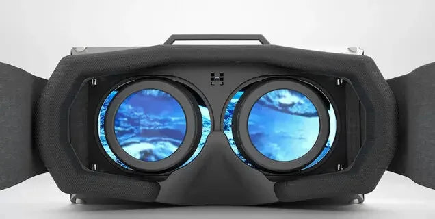
Because Micro OLED screens are extremely small (typically 0.5 to 1.3 inches), they pair perfectly with Pancake optical modules.
In this scheme, the high PPI screen acts as a point light source, maintaining extremely high resolution at the center of the image even after multiple lens folds.
In contrast, if a low PPI screen is used with such optical modules, pixels at the edges would be stretched, leading to image blur.
The massive amount of data points provided by Micro OLED provides sufficient redundant pixels for optical distortion correction, maintaining 1080P-level sensory precision even after edge stretching.
| Performance Indicator | LCD Solution | Traditional OLED | Micro OLED Solution |
|---|---|---|---|
| Sub-pixel Arrangement | Obvious physical grid | Diamond/PenTile | High-precision stripe/square |
| Theoretical PPD Limit | 20 - 30 PPD | 30 - 45 PPD | 60 - 120 PPD |
| Screen-door Effect | Severe (clear grid) | Medium (grainy) | Almost invisible |
| Edge Text Resolution | Blurry | Color fringing | Sharp and clear |
On glass substrates, long signal lines suffer from voltage drop (IR Drop) due to resistivity, leading to uneven brightness on large screens.
On 12-inch silicon wafers, multi-layer metal interconnects ensure each micrometer-scale pixel receives precise voltage control.
This circuit-level integration allows grayscale control for each pixel to reach the 1-billion-color level.
Even at 4000 PPI, the brightness error of each pixel can be controlled within 1%, ensuring no blocky noise or uneven stripes appear in dark scenes.
High pixel density is strongly correlated with lightweight design.
Because pixels are small enough, achieving 4K resolution only requires a display module of about 1.3 inches, allowing the total weight of the headset's display front-end to be kept under 50 grams.
If traditional technology were used, achieving the same resolution would require a panel over 3.5 inches, increasing optical module volume, shifting the center of gravity forward, and increasing pressure on the face.
The ability of Micro OLED to stack high-density information in tiny spaces is the technical support for achieving AR devices that resemble ordinary glasses.
Millisecond Response Feedback
In LCD screens, liquid crystal molecules need to physically rotate to change light transmission, a process taking 1 ms to 5 ms.
In contrast, Micro OLED is self-emissive, with each pixel controlled by the underlying CMOS circuit.
When a voltage signal arrives, the organic emitting layer generates photons instantaneously, with a grayscale response time typically under 10 microseconds (0.01 ms).
In headset sensory experience, Motion-to-Photon (MTP) Latency is the standard of quality.
This includes sensor acquisition, processor calculation, GPU rendering, and screen output. To avoid motion sickness, the total latency must be under 20 ms.
If the display's response time takes 5 ms, the remaining budget for rendering and sensors becomes very tight.
Micro OLED's near-zero latency compresses the display portion to a negligible level, giving the system more time for high-precision tracking and rendering, physically reducing discomfort caused by visual drift.
| Display Technology Type | Typical Response (ms) | Speed Multiplier (vs LCD) | Effect on Motion |
|---|---|---|---|
| Traditional LCD (IPS/VA) | 2ms - 10ms | 1x | Obvious motion blur |
| Gaming Fast-LCD | 1ms - 0.5ms | 10x | Slight ghosting |
| Standard Glass OLED | 0.1ms | 50x | Clear image |
| Micro OLED (Silicon) | Below 0.01ms | 500x+ | Completely blur-free |
When refresh rates reach 90Hz or 120Hz, every Micro OLED pixel can completely finish its state switch before the next frame arrives.
Operators see sharp frames without image tearing or sensory lag during rapid head movements.
This feedback comes from complex active-matrix driving, where each pixel has dedicated storage capacitors and control transistors on the CMOS backplane.
Signals don't wait for long scans; pixels work synchronously with extreme precision.
- Black Frame Insertion (BFI): Due to fast response, the screen can insert extremely short black frames between active frames, eliminating retinal persistence and making motion look smoother than the actual refresh rate.
- Global Shutter Effect: In high-spec modules, all pixels can switch nearly simultaneously, avoiding the "rolling shutter" skewing of traditional line-by-line scanning.
- Pulse Width Modulation (PWM): Controls brightness via emission duration. At millisecond frequencies, this is imperceptible to the human eye and avoids low-frequency flicker that causes eye fatigue.
In low-light or high-contrast scenes, Micro OLED's advantage grows. Glass-based OLEDs often lag when switching from pure black to dark gray, causing "Black Smear."
Micro OLED's monocrystalline silicon drive is stronger, accurately controlling pixel activation at tiny currents, ensuring that even at 100,000:1 contrast, small white dots moving across black backgrounds leave no visual trace.
| Performance Dimension | LCD Solution Performance | Micro OLED Performance |
|---|---|---|
| Motion Blur | Severe (needs backlight strobing) | Minimal (native high sharpness) |
| Ghosting | Common in high-refresh scenes | Physically eliminated |
| Black Level Switch Speed | Very slow (LC viscosity) | Instantaneous (electrical excitation) |
| Synchronization | Has line delay | Highly synchronous |
If AR virtual markers lack millisecond refresh during rapid movement, they drift relative to real objects.
Micro OLED, paired with high-frequency sensors (like 1000Hz IMUs), achieves real-time alignment.
This precision is essential for industrial maintenance circuit labeling or surgical incision positioning.
From an integration standpoint, the fast response allows for leaner buffer strategies in display ICs, reducing component stacking, heat loss, and weight.
Mainstream 0.7-inch modules now have display logic latency stabilized at the 5-microsecond level, providing ample bandwidth for high-frequency output above 120fps.
AR/VR Applications
Micro OLED achieved 23 million pixels per eye in Apple Vision Pro, with PPD reaching 40.
Compared to Meta Quest 3's LCD, contrast improved from 1000:1 to 100,000:1.
This 0.7-inch panel outputs 3000 nits, reducing device thickness by over 30% when paired with Pancake optics, making it the technology of choice for high-end immersive headsets.
Wearable Devices
Unlike traditional glass-based LCD or OLED, Micro OLED builds drive circuits directly on 12-inch silicon wafers via CMOS processes, shrinking pixel pitch to 4–8 micrometers.
Within a 1.3-inch area, it can accommodate 3840 by 2160 resolution or higher, with PPI typically between 3000 and 4500.
This leap in physical properties allows wearables to reach 40–60 PPD, effectively eliminating the "screen-door effect."
- Module Thickness: The silicon backplane is usually under 1 mm, reducing display assembly thickness by 80% compared to backlit LCDs.
- Optical Path Shortening: Pair with Pancake optics to compress headset thickness from 60mm to under 30mm, bringing the center of gravity closer to the face.
- Weight Distribution: A single module weighs less than 5g, leaving more room for cooling and battery weight management.
With self-emissive mechanisms, each pixel is independent, allowing contrast to exceed 1,000,000:1.
This supports over 95% DCI-P3 coverage and 10-bit color depth.
For high-brightness AR, peak brightness can break 5000 nits, ensuring that even after 80% loss through waveguides, effective brightness remains over 500 nits.
- Power Control: When displaying dark content, single-panel power consumption is maintained between 100 to 300 mW, saving 30%–50% power vs LCD.
- Refresh & Latency: Supports up to 144Hz with response times shortened to 10 μs, 200 times faster than liquid crystal.
- Thermal Adaptability: Silicon circuits don't suffer from mobility drops at -20°C like glass circuits do.
Surgical Procedures
Micro OLED is shifting surgical vision from 2D monitors to high-res near-eye displays.
Integrating CMOS on silicon allows 3840 by 2160 pixels in 0.7 inches.
For surgical HMDs, PPD reaches 40+, exceeding human resolution limits at close range.
Surgeons can clearly see nerve branches or vessel walls under 0.05 mm in diameter without pixelation.
- Color Accuracy: 10-bit color ensures doctors can distinguish tissue pathologies via subtle color differences.
- Low Latency: 0.01 ms response reduces ghosting during micro-manipulation.
- Brightness: 3000–5000 nits ensure AR overlays remain visible under intense surgical lighting.
The 0-nit black level is crucial for merging virtual and reality.
When 3D tumor models are overlaid on real anatomy, there is no "halo" effect. MTP latency under 10 ms ensures tool movement and digital markers are perfectly synced.
- Lightweight: Total headset weight can be under 500g with Pancake optics.
- Energy: 150–300 mW power reduces heat, avoiding the need for noisy cooling fans in sterile environments.
- Work Stability: High EMI resistance ensures the screen doesn't flicker when using high-frequency electrosurgical units.
Industrial Maintenance
In industrial digital transformation, Micro OLED provides 2560 by 1440 matrices in 0.5-inch areas.
This shrinking of pixel pitch to 4–6 μm keeps PPD between 35 and 45. Technicians can see 3D CAD disassembly models overlaid on real engine parts via waveguides.
High resolution ensures that part numbers and torque values remain readable even during slight head movements.
| Industrial Parameter | Traditional LCoS | Silicon Micro OLED | Impact on Maintenance |
|---|---|---|---|
| Peak Brightness | 1000 - 2000 nits | 3000 - 10000 nits | Visibility in outdoor sunlight |
| Contrast | 1000:1 | 100,000:1+ | AR info won't block the real view |
| Power | 500 - 800 mW | 100 - 300 mW | Supports full 8-hour shifts |
| Response Time | 2 ms | 0.01 ms | Reduced lag during rapid machinery checks |
| Temp Range | 0 to 50 °C | -20 to 70 °C | Adapts to extreme industrial environments |
MLA technology allows brightness to break 5000 nits. Even with 10% efficiency in diffraction waveguides, effective brightness remains over 500 nits for outdoor use.
Lightweight design (under 70g for the whole AR glass) reduces pressure on the nose during long inspections.
Integrated MIPI/eDP interfaces allow real-time sensor data (temp, RPM) to appear with under 10ms delay, enabling "look-and-repair" workflows that shorten diagnosis time by 30%–40%.
Read more
Micro OLED features 3000+ PPI and 5000 nit brightness, completely eliminating the screen-door effect; The 0.01 ms ultra-fast response time solves motion sickness, serving as the performance benchma...
COG (Chip-on-Glass) directly bonds the IC to the glass, thinning the module by more than 30% and refining the lead pitch to 40μm. Its streamlined structure reduces costs by approximately 20% and si...
Leave a comment
This site is protected by hCaptcha and the hCaptcha Privacy Policy and Terms of Service apply.