


Transparent OLED Displays | Transmittance Rate, Brightness & AR Applications
Transparent OLED has a transmittance rate of 38%-50% and a peak brightness of about 600 nits.
It drives the pixels to self-illuminate through transparent electrodes. In AR applications, it controls color brightness by adjusting the driving current, allowing virtual images to be accurately superimposed on the real scene.
Achieving high-contrast interaction at 40% transparency, it is an ideal solution for smart display windows and automotive HUDs.
Transmittance Rate
T-OLED panels achieve a system-level transmittance rate of 38% to 45% through a 40% pixel aperture ratio.
Its structure mainly consists of a 15-nanometer-thick magnesium-silver alloy cathode and a highly transparent ITO anode, which reduces light absorption while ensuring current conduction.
Compared to the 10% transmittance level of traditional transparent LCDs, T-OLED reduces the over 50% light loss caused by polarizers, keeping the visual clarity loss of background objects below a 1.5% haze value.
Pixel Spatial Layout
In a standard 55-inch FHD transparent panel, the individual pixel size is approximately 635μm x 635μm. To achieve a 40% system transmittance rate, the transparent window area must occupy about 254,000 square micrometers to ensure light can pass through unhindered.
Engineers compress all opaque Low-Temperature Polycrystalline Silicon (LTPS) circuits and storage capacitors (Cst) directly beneath the projection of the light-emitting area. In this vertically stacked architecture, the vertical overlap error of metal traces must be controlled within ±1μm to free up the maximum possible net space for the transparent window.
| Space Allocation Dimension | Emissive Area (EA) | Transparent Area (TA) |
|---|---|---|
| Physical Area Proportion | 35% - 38% | 62% - 65% |
| Main Components | Organic materials, TFT circuits, metal cathode | Only substrate glass and passivation layer retained |
| Optical Transmittance | Approx. 5% (blocked by metal) | Approx. 88% - 92% |
| Functional Goal | Output brightness above 600 nits | Maintain background haze value below 1.5% |
Regarding sub-pixel layout, T-OLED usually abandons the traditional RGB stripe arrangement in favor of a compact "island-style" cluster. The organic evaporation layers of the three primary colors, Red, Green, and Blue (RGB), are confined within the light-emitting area. For highly energy-efficient display solutions, the green sub-pixel area is typically 20% larger than the blue one, because green materials have higher luminous intensity at a 525nm wavelength.
To connect these distributed pixel islands, Data Lines and Gate Lines must shuttle along the edges of the transparent areas. These traces are made of Molybdenum (Mo) or Aluminum (Al), with line widths refined to 5μm. On a panel with a 120Hz refresh rate, to reduce signal delay (RC Delay), the trace thickness must be maintained at 300nm.
-
Pixel Pitch: On a large screen with 40 PPI, the pixel pitch is 635μm, providing good continuity for the transparent area.
-
Metal Shielding Rate: The opaque metal coverage area within each square millimeter must be less than 0.4mm².
-
Diffraction Control: The edges of the transparent areas are designed as arcs or irregular polygons to reduce diffraction patterns generated when light passes through the gaps.
-
Aperture Ratio: The effective aperture area (Aperture Ratio) of the light-emitting area is typically only 15% to 22%.
-
Electrode Overlap: The overlap area between the cathode and anode in the transparent area must approach 0.
When the pixel density increases to 300 PPI (such as a 10-inch tablet prototype), a single pixel shrinks to an 84μm square. At this point, the physical volume of the driving circuit cannot be proportionally reduced, causing the proportion of the transparent area to plummet below 20%. This dynamic adjustment of spatial layout indicates that there is a 2.5x negative correlation weight coefficient between high transparency and high resolution under the current physical framework.
If the boundaries of the transparent areas are too regular, an obvious "grid effect" will occur under 5000 lux of strong light exposure. To address this, high-end panels add an Index Matching Layer (RIM) to the edges of the transparent area. The refractive index of this material is 1.6, which smooths the optical transition between the transparent and light-shielding areas, reducing the visual striped sensation by 30%.
-
Vertical Shielding Layout: Hide all sensors and traces directly beneath the organic light-emitting materials to maximize the transparent aperture.
-
Asymmetric Sub-pixels: Blue sub-pixels use an elongated shape to adapt to current density, while red ones use a square shape to optimize space utilization.
-
Trace Intensification: Adopt shared loop technology to merge the ground lines (VSS) of two columns of pixels, saving 8μm of lateral space.
In the multilayer film stack, the Hole Blocking Layer (HBL) and Electron Blocking Layer (EBL) inside the transparent area are etched away. Through the Plasma Dry Etching process, organic residues within the transparent window are cleaned to a thickness below 10 nanometers. This step prevents the physical deformation of organic materials caused by absorbing heat after long periods of operation, ensuring the long-term flatness of the window.
| Resolution Specification | Total Pixels (FHD) | Total Emissive Area | Total Transparent Window Area |
|---|---|---|---|
| 55" Panel | 2,073,600 | Approx. 0.42 m² | Approx. 0.81 m² |
| 30" Panel | 2,073,600 | Approx. 0.12 m² | Approx. 0.15 m² |
| Trend | Constant area | Proportion increases with PPI | Proportion decreases with PPI |
A circular Emissive Island provides a more uniform electric field distribution compared to a rectangular one, thereby extending the luminous lifespan of organic molecules by 15%. In the layout design, the width of the Black Matrix between adjacent pixel islands is compressed to within 10μm. Visually, this prevents a "floating sensation" of the image pixels, allowing digital images to deeply integrate with the background physical space.
Film Material Specifications
T-OLED panels integrate over 15 functional film layers within a total thickness of 0.7mm. The bottom layer uses 0.5mm borosilicate glass or a flexible PI substrate, whose transmittance must be maintained above 91.8%. The anode layer uses 100nm thick Indium Tin Oxide (ITO). This transparent conductive oxide has a light absorption rate of less than 2% at a 550nm wavelength, while possessing a low sheet resistance characteristic of 15Ω/sq to ensure hole injection efficiency.
| Film Component | Thickness Specification | Optical Contribution / Physical Properties |
|---|---|---|
| ITO Anode | 80 - 120 nm | Refractive index approx. 1.8, Light transmittance >98% |
| Organic Emissive Layer | 150 - 200 nm | Includes 4-layer structure: HIL/HTL/EML/ETL |
| Semi-transparent Cathode | 10 - 20 nm | Magnesium-silver alloy (Mg:Ag) ratio is typically 10:1 |
| CPL Capping Layer | 60 - 80 nm | Adjusts optical interference, enhances light extraction efficiency by 20% |
Inside the organic stack, the thickness of the Hole Transport Layer (HTL) and Electron Transport Layer (ETL) is accurate to the 1 Angstrom (Å) level. To prevent color shift caused by the microcavity effect, the thermal stability temperature of the organic molecules in the Emission Layer (EML) must exceed 350°C. For transparency optimization, the evaporation process needs to control organic residues in non-emissive areas below 0.5% to avoid blurred images caused by scattered light.
-
Mg:Ag Alloy Ratio: The cathode uses a mixture of 90% magnesium and 10% silver, where silver provides conductivity and magnesium lowers power consumption.
-
Ultra-thinning Treatment: When the thickness is reduced from 25nm to 15nm, transmittance can jump from 65% to 82%.
-
Work Function Matching: The cathode work function needs to be maintained around 3.7eV to lower the electron injection barrier.
-
Lossless Evaporation: Physical Vapor Deposition (PVD) is used, with the evaporation rate controlled at 0.1nm/s to ensure film flatness.
To further protect the sensitive organic materials, a Thin Film Encapsulation (TFE) system covers the top. This system alternately consists of inorganic silicon nitride (SiNx) and organic monomers. The thickness of a single SiNx layer is about 1μm, which can provide a water and oxygen barrier rate of 10^-6 g/m²/day.
-
SiNx Inorganic Layer: Uses Plasma-Enhanced Chemical Vapor Deposition (PECVD), with a refractive index targeted at 1.9.
-
IJP Organic Layer: Filled via inkjet printing technology, with flatness errors controlled within 20nm.
-
Multi-stage Stacking: Typically adopts a 2-pair (4-layer) cyclic structure to resist external scratches and chemical erosion.
At the top of the encapsulation layer, the CPL (Capping Layer) acts as an optical regulator. By using high-refractive-index materials with an index greater than 2.0, the CPL can alter the total internal reflection path, allowing more photons to shoot towards the user side, thereby increasing panel brightness by 15% to 25% without increasing power consumption. This film layer also has a UV filtering function, blocking UV bands below 380nm to prevent organic material aging.
| Metric | Traditional Metal Cathode | T-OLED Semi-transparent Cathode |
|---|---|---|
| Transmittance (T%) | < 1% | 75% - 85% |
| Surface Resistance | 1 - 2 Ω/sq | 10 - 20 Ω/sq |
| Visible Light Reflection | > 90% | < 15% |
| Thickness Control | 100 - 300 nm | 10 - 25 nm |
To eliminate visual interference from ambient light, a 100μm thick Anti-Reflection (AR) film is laminated to the outermost layer of the panel. This nano-level interference film utilizes alternating stacks of multiple layers of silicon dioxide (SiO2) and niobium pentoxide (Nb2O5) to reduce the reflectance of the glass surface from 4.5% to 0.5%. This ensures that the color reproduction of background objects remains above 95% in a 1000 lux lighting environment.
-
SiO2 Film Layer: Refractive index 1.46, mainly responsible for reducing the reflection intensity of high-frequency light.
-
Nb2O5 Film Layer: Refractive index 2.30, cooperates with low-refractive-index materials to build destructive interference.
-
Hydrophobic Coating: The outermost layer undergoes fluorination treatment, achieving a contact angle greater than 110° to prevent oil and stain adhesion.
Impact of Pixel Density
Taking a 55-inch commercial transparent panel as an example, its resolution is set at 1920 x 1080, and the corresponding pixel pitch is about 635 micrometers. Under this low-density layout, the panel can spare over 60% of the space as a transparent window, thereby maintaining a light penetration rate of over 40%.
When the display size is reduced to 13 inches and attempts to achieve 2K resolution, the pixel density will soar to over 220 PPI. At this time, a single pixel size shrinks to about 115 micrometers. Because the Thin Film Transistor (TFT) circuits and metal capacitors driving the pixels have physical volume limits and cannot shrink proportionally with the pixels, the proportion of the transparent area will quickly shrink to around 20%.
Experimental data shows that when the pixel density increases from 40 PPI to 100 PPI, the average transmittance of the panel drops by about 12.5%. This decrease is not due to changes in glass transparency, but because the length of opaque metal traces per unit area increases by 2.5 times, causing a massive expansion of the light-shielding area.
-
Trace Obstruction Rate: In a high-resolution design of 300 PPI, the total width of data lines and power lines occupies 18% of the pixel gap.
-
Capacitor Volume: To maintain voltage stability at a 60Hz refresh rate, the storage capacitor (Cst) must occupy about 1500 square micrometers of opaque space.
-
Alignment Precision Limits: The alignment error of Fine Metal Masks (FMM) in production is ±3 micrometers, and high PPI requires wider protective edges, further squeezing the transparent area.
-
Pixel Island Shape: As PPI increases, the pixel emissive island transitions from a square to a slender strip to reduce the cutting of lateral transparent space.
When the aperture width of the transparent window drops below 50 micrometers, obvious physical diffraction will occur with the ambient light passing through the screen. When users observe background objects, rainbow-like dispersion stripes will appear at the edges of the objects. This phenomenon is particularly significant in bright environments where illumination exceeds 2000 lux.
Physical measurements indicate that on a 200 PPI transparent panel, the visual haze of background objects will rise from 1.2% at low density to 4.8%. The clarity of the background no longer depends solely on the transmittance value, but is heavily influenced by the optical diffraction interference brought by pixel fineness.
-
Current Density Challenge: To maintain a brightness of 600 nits at high PPI, due to the reduced emissive area, the current density of the organic materials needs to be increased by 3 times.
-
Heat Accumulation: Dense pixels concentrate heat output. If the local temperature exceeds 65°C, the oxidation decay rate of organic molecules will accelerate.
-
Aperture Ratio Loss: The physical aperture ratio is typically below 12% at 400 PPI, which is seen as the current technical ceiling for the commercialization of T-OLED.
-
Diffraction Fringes: The 0th and 1st order diffraction spots formed by ambient light passing through narrow slits reduce background contrast by about 15%.
To reduce the number of opaque traces, engineers introduced a 2-TFT driving architecture. Although this design streamlines space, it increases the difficulty of controlling current uniformity. Under the display requirement of 12-bit color depth, this spatial compression leads to a brightness deviation between different pixels of over 3%.
For AR Head-Up Display applications, panels typically select a medium density of 80 to 120 PPI. This range can provide sufficient image details while maintaining background transmittance between 30% and 35%, ensuring that the driver's recognition rate of road obstacles ahead drops by less than 2%.
-
Signal Delay (RC Delay): Thinner traces lead to higher resistance, which causes smearing at the image edges at high refresh rates.
-
Multi-layer Wiring: By introducing more than 3 metal connection layers to overlap some traces, 5% of the transparent area can be freed up.
-
Electromagnetic Interference: Shrinking pixel pitch enhances signal interference, requiring a 1-micrometer-wide grounded shielding layer between traces.
With the same display content, a 200 PPI transparent screen consumes about 45% more power than a 40 PPI screen. The reason is that smaller emissive apertures require higher driving voltages to overcome internal resistance and pump photons out of the roughly 200-nanometer thick organic film layer, directly leading to an increase in battery drain or the thermal load on the power module.
Industry standard calculations show that for every 10% increase in pixel density, while maintaining the same perceived backlight brightness, the system's total conversion efficiency (lm/W) decreases by about 7%. This forces high-PPI transparent screens to adopt more efficient phosphorescent materials or multi-stack (Tandem) structures to compensate for optical losses.
Maintaining 150 PPI in the user's central visual area ensures text clarity, while reducing to 60 PPI in the peripheral areas enhances the overall sense of transparency. This zone-based layout logic can boost the overall average transmittance of the machine by 8%, while simultaneously alleviating the computational load on the back-end data driving circuits.
| Pixel Density (PPI) | Single Pixel Width (μm) | Suggested Transparent Area Proportion (%) | Measured Transmittance (T%) |
|---|---|---|---|
| 40 (55" FHD) | 635 | 65% | 42% |
| 80 (32" 4K) | 317 | 50% | 31% |
| 160 (15" 2K) | 158 | 35% | 22% |
| 320 (Mobile) | 79 | 15% | 11% |
When performing ultra-high-density organic vapor deposition on 0.5mm glass, any dust particle exceeding 0.5 micrometers in diameter will directly obscure the transparent window or cause a pixel short circuit. On a 300 PPI panel, the proportion of fatal defects caused by such micro-flaws is 4.5 times higher than on a low-density panel, significantly driving up the manufacturing cost per unit of display area.
Under these physical constraints, the current transparent OLED market leans mainly towards large-sized, low-PPI devices. By maintaining a lower pixel density, the panel can retain enough transparent channels so that light still has a sufficient margin to reach the human eye after passing through 15 film layers.
Brightness Metrics
The brightness output of transparent OLEDs is usually between 150 and 600 nits. Taking a mainstream 55-inch T-OLED panel as an example, the full-screen sustained brightness is about 150 nits, while the local peak brightness can reach 600 nits at 1% APL.
This is directly related to the 40% physical transmittance: the smaller the space occupied by the light-emitting sub-pixels, the better the light penetration, but the total light emission per unit area decreases.
For AR (Augmented Reality) devices, because optical waveguide components have a 90% light loss, the screen source brightness must exceed 3000 nits to ensure outdoor visibility.
Pixel Structure Principles
Using a 55-inch 4K panel as an example, the physical size of a single pixel is about 0.315 millimeters, of which about 60% of the space is reserved as a pure transparent window. Light can penetrate multiple layers of glass and organic films in this structure to achieve an overall transmittance of around 40%.
Inside the light-emitting area lies a stacked organic architecture consisting of a Hole Transport Layer (HTL), Emission Layer (EML), and Electron Transport Layer (ETL). The thickness of these films is typically between 100 and 300 nanometers, and photoelectric conversion efficiency is tuned by precisely controlling the thickness of each layer. When a current passes through at a voltage of 3.7V to 4.5V, organic molecules are excited to emit photons, with an internal quantum efficiency approaching 100% in a laboratory environment.
To ensure light can shoot out from the front, the anode usually uses 150 nanometer thick Indium Tin Oxide (ITO), while the cathode must balance conductivity and transparency. Currently, the industry generally uses ultra-thin metallic silver or magnesium-aluminum alloy with a thickness of less than 10 nanometers. This ultra-thin metal layer can keep the sheet resistance below 10 ohms/square while guaranteeing a 85% visible light penetration rate, preventing image blurring caused by metal reflection.
The following table shows the typical physical parameters and optical losses of the internal layers of a transparent panel:
| Structure Layer Name | Typical Thickness (nm) | Material Characteristics | Optical Transmittance (%) |
|---|---|---|---|
| Glass Substrate | 500,000 | Borosilicate glass | 92% |
| ITO Anode Layer | 150 | Transparent conductive oxide | 90% |
| Organic Emissive Stack | 250 | Multilayer polymers/small molecules | 75% |
| Ultra-thin Metal Cathode | 8 | Silver/magnesium alloy film | 88% |
| Thin Film Encapsulation (TFE) | 3,000 | Silicon nitride/organic monomer | 98% |
The underlying driving circuit uses Low-Temperature Polycrystalline Oxide (LTPO) technology, which pushes transistor carrier mobility above 50 cm²/Vs. High-performance transistors can reduce physical volume to below 20 micrometers and hide beneath the opaque light-emitting pixels. Through this vertically stacked solution, the transparent area maintains 100% purity, avoiding physical obstruction of the background view by metal traces.
These tiny circuit traces typically use a metal sandwich structure composed of Molybdenum/Aluminum/Molybdenum (Mo/Al/Mo). To suppress the "rainbow fringes" caused by light diffraction, the width of the wires is strictly limited to within 3 micrometers. In a 3840 x 2160 pixel array, several kilometers of fine wires are neatly arranged to ensure that no grid sensation is detectable to the naked eye at a typical viewing distance of 1 meter.
This high-integration design requires extremely small gaps between sub-pixels, usually set at around 5 micrometers. The tiny gap prevents electrical crosstalk between pixels and ensures that under a 120Hz refresh rate, the precision error of charge injection and release is below 1%. This also causes the current density of T-OLED to be more than twice that of ordinary panels, requiring rapid heat dissipation through a substrate with a thermal conductivity of 1.1 W/m·K.
Here are several key technical features of the physical layout of transparent pixels:
-
Aperture Ratio Allocation: Emissive area accounts for 35% - 40%, transparent area accounts for 55% - 60%, and the rest is circuit footprint.
-
Sub-pixel Density: A 55-inch panel is about 80 PPI, meeting the visual needs of commercial displays and close-range interactions.
-
Encapsulation Thickness: Uses Thin Film Encapsulation (TFE), with a total thickness of only 3 micrometers to prevent moisture penetration.
-
Water and Oxygen Barrier Rate: Reaches 10^-6 g/m²/day, ensuring organic materials do not fail within 30,000 hours.
-
Trace Precision: Uses FMM (Fine Metal Mask), with mask alignment deviation controlled within ±2 micrometers.
-
Refractive Index Matching: The refractive index difference at interface layers is controlled within 0.1 to reduce optical losses caused by internal total reflection.
Because the emissive layer is confined to a narrow area, outputting a brightness of 600 nits places a very high instantaneous current load on a single sub-pixel. To mitigate physical degradation of organic materials at high temperatures, high-performance panels are beginning to introduce Tandem structures. This structure vertically connects two emissive units in series via a Charge Generation Layer (CGL), increasing brightness output by 1 time under the same current while reducing driving heat by 20%.
When producing these precision pixels, Vapor Phase Deposition (VPD) technology must be used in ultra-clean room environments of Class 10 or above. The organic material deposition thickness deviation for each pixel cannot exceed 5 Angstroms (about 0.5 nanometers). This atomic-level control precision ensures full-screen brightness uniformity above 95%, meaning transparent screens will not display color fluctuations visible to the naked eye when showing a solid-color background.
The Micro-OLED structure geared for AR applications goes a step further by compressing pixel pitch to the micrometer level, achieving densities over 4000 PPI. These devices are usually manufactured on 300-millimeter silicon wafers, using semiconductor lithography processes to define pixels. Their proportion of transparent windows is typically sacrificed in exchange for extremely high peak brightness, to offset the massive loss of light energy refraction brought by the optical waveguide near-eye system.
The differences in pixel performance across different production lines and technical routes are shown in the table below:
| Technology Process | Typical Pixel Density (PPI) | Minimum Trace Width (μm) | Max Aperture Ratio (%) | Target Application Field |
|---|---|---|---|---|
| Gen 8.5 Line (WOLED) | 80 - 100 | 3 - 5 | 40% | Large commercial windows |
| Gen 6 Line (RGB) | 150 - 300 | 1 - 2 | 35% | Smartphones/Tablets |
| Silicon-based (Micro-OLED) | 3000 - 5000 | < 0.5 | 20% (High brightness priority) | AR/VR visual hardware |
By forming a Micro Lens Array (MLA) on the surface of the encapsulation layer, light that was originally unable to shoot out from inside the glass layer due to refractive index differences can be redirected to the front. This optical repair method has increased the panel's light extraction efficiency by 22%, effectively lowering the initial current required to maintain high brightness and significantly optimizing the display's long-term power consumption.
Current materials science is dedicated to finding more transparent electrode candidates than silver, such as Carbon Nanotubes (CNTs) or new conductive polymers. These materials have a light absorption rate of less than 1% at a 550-nanometer wavelength, enabling the transmittance of the transparent area to march towards 50%. As these materials enter mass production testing, transparent OLEDs will be able to achieve a more realistic fusion of virtual and real effects, eliminating the slight hazy sensation that currently exists.
Scenario Brightness Comparison
In high-end brand stores in Paris or New York, a 55-inch transparent panel needs to reach 450 nits at 10% APL (Average Picture Level) to offset the interference of an average 800 lux indoor spotlighting. If the brightness is lower than 150 nits, the image will produce obvious semi-transparent ghosting against a white background, making 4K resolution details almost unrecognizable from 2 meters away. Micro-OLED chips in the AR field are usually only 0.49 inches, but their source brightness must be pushed to 5000 nits because optical waveguide lenses lose over 90% of the lumen output during transmission.
When a train travels from a tunnel to the surface, the external ambient light instantly surges from 50 lux to over 10,000 lux. To ensure passengers can clearly see station information on the screen, the panel's sustained brightness must stabilize between 600 nits and 800 nits. Maintaining this brightness relies on 1.5mm thick toughened glass for heat dissipation support, ensuring the organic materials do not suffer rapid degradation under extreme operating environments of 70 degrees Celsius.
Display units in the aforementioned environments typically meet the following parameter standards:
-
Full-screen White Brightness: Stabilized at 150 - 200 nits, avoiding power overload caused by large-area light emission.
-
Contrast Performance: Reaches 100,000:1 in dark environments, presenting pure black pixels.
-
Refresh Rate Metric: Uniformly uses 120Hz, reducing smearing effects in fast-moving images.
-
Pixel Pitch: Controlled within 0.6mm, ensuring no grid sensation when viewed up close.
-
Power Consumption Control: A 55-inch panel consumes about 65W at peak brightness, superior to transparent LCDs of the same size.
-
Operating Voltage: Driving circuits typically operate in a DC environment of 12V to 24V.
In F-35 pilot helmets or high-end industrial AR headsets, the sub-pixel density of Micro-OLED exceeds 4000 PPI. Because the light-emitting points are extremely small, each sub-pixel bears a current density more than 50 times that of ordinary TV panels. To output 500 nits of final in-eye brightness under direct sunlight, the underlying architecture must use a Tandem structure, increasing photoelectric conversion rates through the superposition of two layers of light-emitting materials.
The following table shows the data relationship between brightness and environments in mainstream industry applications abroad:
| Application Physical Space | Ambient Light Intensity (Lux) | Target Panel Brightness (Nits) | Transmittance Percentage |
|---|---|---|---|
| New York Commercial Window | 500 - 1,500 | 450 - 550 | 38% - 40% |
| London Underground Side Window | 50 - 10,000 | 600 - 800 | 30% - 35% |
| Silicon Valley Office Partition | 200 - 400 | 150 - 250 | 45% - 52% |
| Outdoor AR Navigation | 30,000+ (Sunny day) | 3,000 - 5,000 | >85% (Lens) |
In meeting rooms at Canary Wharf, London, the brightness of transparent display walls is usually restricted to around 250 nits. Excessive brightness causes visual fatigue for observers due to multiple light refractions on the glass surface. At this point, the circuit design focuses on the PWM dimming frequency, which generally needs to be higher than 1920Hz to eliminate flicker that is invisible to the naked eye but causes eye discomfort.
Specific office scenarios typically add a layer of dynamic dimming film to assist in brightness performance:
-
Automatic Light Sensing Adjustment: Sensors collect ambient light data 60 times per second to fine-tune panel current intensity in real time.
-
Contrast Enhancement: When external light is too strong, the dimming film adds 20% haze, artificially increasing the image's sense of depth.
-
Color Calibration System: Performs 10-bit mapping tailored to the DCI-P3 color gamut, ensuring colors do not distort under 200 nits.
In panels produced by Gen 8.5 lines, the resistivity of Silver Nanowires (AgNWs) electrodes is reduced by 15% compared to traditional ITO. Optimizing this parameter allows more current to pass without generating excessive heat loss, keeping sustained brightness fluctuations within a range of ±5%.
Brightness Enhancement Technologies
The luminous efficiency of transparent OLEDs is strictly limited by the physical aperture ratio, as 60% of pixel space must remain transparent. To squeeze higher lumens out of the remaining 40% emissive area, the industry widely adopts a Multi-layer Tandem OLED architecture. This structure vertically stacks two or even three emissive units via a Charge Generation Layer (CGL), allowing the panel to achieve doubled brightness and a 30% reduction in power consumption under a driving voltage of 5V to 8V.
In a traditional single-layer structure, achieving a peak brightness of 600 nits requires organic materials to endure extremely high current loads. With a tandem structure, each layer only needs to bear half the brightness output, which extends the lifespan of blue-light organic materials by over 3 times. According to testing data from overseas laboratories, a 55-inch panel using this technology can keep brightness degradation within 5% after continuous operation for 30,000 hours.
Tandem Architecture Core Data Metrics:
Driving Voltage: Increased by about 1.8 times compared to single-layer structures, but luminous efficiency (cd/A) increases by 2 times.
Color Purity: The use of materials with narrow Full Width at Half Maximum (FWHM) pushes the DCI-P3 color gamut coverage to 98%.
Thermal Power Control: Under the same brightness, the panel center temperature is 5 degrees Celsius lower than that of a single-layer structure.
To resolve the loss caused by total internal reflection within the glass substrate, Micro Lens Arrays (MLA) have become a standard solution to boost brightness. By depositing hundreds of millions of micrometer-scale hemispherical lenses above the encapsulation layer, 20% of light energy originally trapped inside the glass due to large refraction angles is redirected toward the observer. This physical optical method directly elevates the panel's light extraction efficiency from 20 lm/W to over 25 lm/W.
The diameters of these micro-lenses are usually controlled between 5 and 10 micrometers and are manufactured using high refractive index (n ≈ 1.8) organic polymers. This process requires the alignment precision between the lens array and the underlying pixels to reach ±1 micrometer; otherwise, severe color shift or viewing angle distortion occurs. In practical applications, introducing MLA technology yields a 22% visual brightness gain for transparent OLEDs without adding extra battery load.
Currently, advanced mass-production lines have begun using Transparent Silver Alloy (Ag) to replace the traditional thick metal cathode. The thickness of this silver alloy is compressed to around 7 nanometers, with an average absorption rate below 5% in the visible light spectrum. The lower sheet resistance (about 8 ohms/square) ensures current is evenly distributed across large display panels, reducing brightness unevenness caused by resistive heating.
Electrode and Encapsulation Technology Parameters:
Cathode Transmittance: Achieves an 88% penetration efficiency at the 550 nanometer wavelength.
Sheet Resistance Performance: Maintained below 10 Ω/sq, supporting rapid switching of large currents.
Reflectance Control: Reduces external environmental reflectance to below 4% through low refractive index encapsulation layers.
Driven by a high refresh rate of 120Hz, charges rapidly fill the organic emissive layer within 8.3 milliseconds, ensuring dynamic images do not suffer from contrast collapse at peak brightness. This highly conductive electrode, paired with an LTPO (Low-Temperature Polycrystalline Oxide) backplane, reduces pixel response time to the 0.1-millisecond level.
For Micro-OLEDs developed for AR hardware, brightness enhancement measures shift toward silicon-based lithography processes. By integrating sub-micron Color Filters and Micro-cavity structures on a single-crystal silicon substrate, photons reflect multiple times inside the emissive layer to generate resonance, thereby significantly narrowing the spectrum and enhancing frontal brightness. This resonance technology can push source brightness beyond 10,000 nits under laboratory conditions.
Tuning this microcavity effect requires controlling organic layer thickness with a precision of 0.5 nanometers. For different R/G/B sub-pixels, microcavity lengths are specifically designed to match the specific wavelengths of each color light. This highly customized physical structure ensures that under the extreme pixel density of 4000 PPI, light energy released by each sub-pixel is precisely collected and aimed at the entrance aperture of the optical waveguide lens.
Micro-OLED High Brightness Technical Features:
Sub-pixel Size: Compressed to within 4 micrometers, supporting the injection of extremely high current density.
Contrast Level: Achieves an infinite contrast ratio exceeding 1,000,000:1.
Driving Capability: Silicon backplane supports ultra-high-speed data throughput of 240 frames per second.
Regarding external light environment management, the addition of Active Matrix Dimming technology provides logic-level support for brightness performance. By compounding a layer of liquid crystal dimming film behind the transparent OLED, the system can change the backplane's transmittance in real-time according to external light intensity. When ambient light reaches 20,000 lux, the dimming film darkens to artificially create a "black background," making an originally 400-nit image visually generate a clarity equivalent to 1500 nits.
The system does not need to run constantly at maximum current, thereby reducing the panel's overall thermal energy loss. In high-end autonomous test vehicles in North America, this technology boosted Head-Up Display (HUD) text legibility under midday sunlight by 40%, while keeping total system power consumption under 15W, substantially lessening the pressure on the vehicle's cooling system.
AR Applications
T-OLED provides a transmittance of 38%-45% and, coupled with a 0.1-millisecond response time, can maintain color performance within a 178-degree viewing angle.
Its 600-nit brightness ensures that under 500 lux of indoor light, superimposed 3D images maintain a 150,000:1 contrast ratio against the real-world background.
With a 120Hz refresh rate, T-OLED reduces visual latency to the millisecond level, meeting the demands of device-free spatial interaction in North American commercial displays.
Smart Transit Windows
Current rail transit and civil aviation aircraft are transitioning from traditional laminated glass to digitized interactive interfaces. Relying on a physical transmittance of 38% to 45%, these transparent OLED panels—less than 2 millimeters thick—successfully embed 1920x1080 pixel dynamic layers into the transparent substrate without altering the load-bearing structure of the window.
When T-OLEDs are installed on the side windows of German high-speed trains (ICE) or the London Underground, glass is no longer merely a physical barrier. Via integrated GPS modules and millisecond-level inertial sensors, running at a 120Hz refresh rate, the system accurately superimposes the train's real-time latitude, longitude, altitude, and digital labels of exterior landmark buildings.
Since the panel uses self-illuminating organic materials, each pixel can independently control light and darkness without the need for a backlight. When external illumination fluctuates between 1000 lux and 5000 lux, the display driver circuit dynamically adjusts peak brightness between 100 and 600 nits based on feedback from external light sensors.
This optoelectronic adjustment mechanism ensures that when passengers view outside scenery, the overlaid 3D maps, station predictions, and Estimated Time of Arrival (ETA) information feature an ultra-high contrast ratio of 150,000:1. Supported by 10-bit color depth, even during high-speed movement, text edge jaggedness and motion blur disappear thanks to the 0.1-millisecond response speed.
| Interactive Function | Hardware Technical Specifications | Actual Operating Parameters |
|---|---|---|
| Geographic Overlay | Real-time RTK positioning correction | Visual alignment error < 3 mm |
| External Brightness Adaptation | Ambient light sensing sync | Dimming response time < 50 ms |
| Multi-point Pressure Touch | Capacitive sensing film | Supports 10 simultaneous touch points |
| Energy Control Efficiency | AOR pixel autonomic technology | Average power 25W/m² |
Beyond surface rail transit, the digitization of portholes in aviation is progressing concurrently. In future concept cabins from Boeing or Airbus, T-OLEDs are sealed between two layers of tempered aviation glass. This structure is compounded at high temperature and pressure using a PVB (Polyvinyl Butyral) interlayer, ensuring stable pressure differentials at altitudes of 30,000 feet.
Through the transparent windshield, pilots acquire not only visibility but also Augmented Reality Head-Up Display (HUD) guidance integrated into the screen. Compared to traditional optical projection HUDs, T-OLED provides an ultra-wide 178-degree viewing angle. Even if the pilot's head shifts slightly, heading, airspeed, and horizon references remain firmly locked into the center of physical line of sight.
Passengers in the cabin can interact via side windows. For instance, when flying over the Grand Canyon, tapping the glass triggers an augmented reality science plugin. The screen pops up geological layering data in a semi-transparent form, while the real mountains in the background remain clearly visible. This pixel-level rendering of mixed reality relies on Oxide Thin Film Transistors (Oxide TFT) integrated into the panel's bottom layer.
-
Real-time Flight Trajectory: Displays current route deviation and remaining distance.
-
Ground Landscape Enhancement: Uses infrared images to supplement vision during night flights.
-
Interactive Menu: Point and select in-flight meals or duty-free goods directly on the window.
-
Digital Shading: Simulates an electronic sunshade by altering the power state of the organic layer.
-
Social Sharing Window: Projects captured sea-of-clouds imagery to fellow cabin passengers in real time.
Turning to urban roads, the digital application on automotive windshields is even more radical. In high-end autonomous testing vehicles in North America, transparent OLEDs are gradually replacing traditional physical dashboards. The panel communicates in real-time with LiDAR via high-speed bus interfaces, outlining the edges of scanned obstacles in fluorescent green lines right on the windshield.
This visual enhancement solution directly shortens driver reaction time because all auxiliary information appears exactly at the driver's natural focal point. When the vehicle reaches 120 km/h, the system processes over 60 frames of complex environmental data per second, ensuring the alignment accuracy of virtual navigation arrows with real lane lines remains above 99.5%.
In the scenario of interior side windows, T-OLEDs transform into mobile digital showrooms. Commuters can browse the daily financial briefing through the window. Benefiting from 150% NTSC color gamut coverage, image saturation can overcome visual dilution caused by intense sunlight, preserving genuine color fidelity.
-
Blind Spot Assist Display: Projects the B-pillar blind spot footage captured by exterior cameras onto the corresponding side window.
-
Dynamic Path Prediction: Projects a virtual driving trajectory onto the ground based on wheel steering angles.
-
Emergency Obstacle Highlight: Boxes suddenly crossing pedestrians or vehicles in red.
-
Parking Interactive Interface: After turning off the engine, the side window transforms into a large office collaboration screen.
-
Biometric Unlocking: Integrates palm vein or fingerprint recognition into specific areas of the window glass.
-
Smart Anti-glare: Performs pixel-level localized dimming against the high beams of rear trailing vehicles.
From a manufacturing standpoint, large-area transit T-OLEDs utilize advanced Mask Deposition Technology. This technique can shrink auxiliary electrode widths down to the micrometer scale while maintaining uniformity across large sizes (such as 55 inches or 77 inches). This ultra-fine trace layout is the physical foundation for sustaining a transmittance of over 40%, avoiding visual gridding.
Targeting extreme external temperature variations, these panels are coated with AR (Anti-Reflection) and AF (Anti-Fingerprint) nano-coatings. These coatings drop external reflectivity below 2% without diminishing screen brightness. Even on sunbaked desert highways or freezing Nordic railways, the panel's chemical stability guarantees a Mean Time Between Failures (MTBF) of over 30,000 hours.
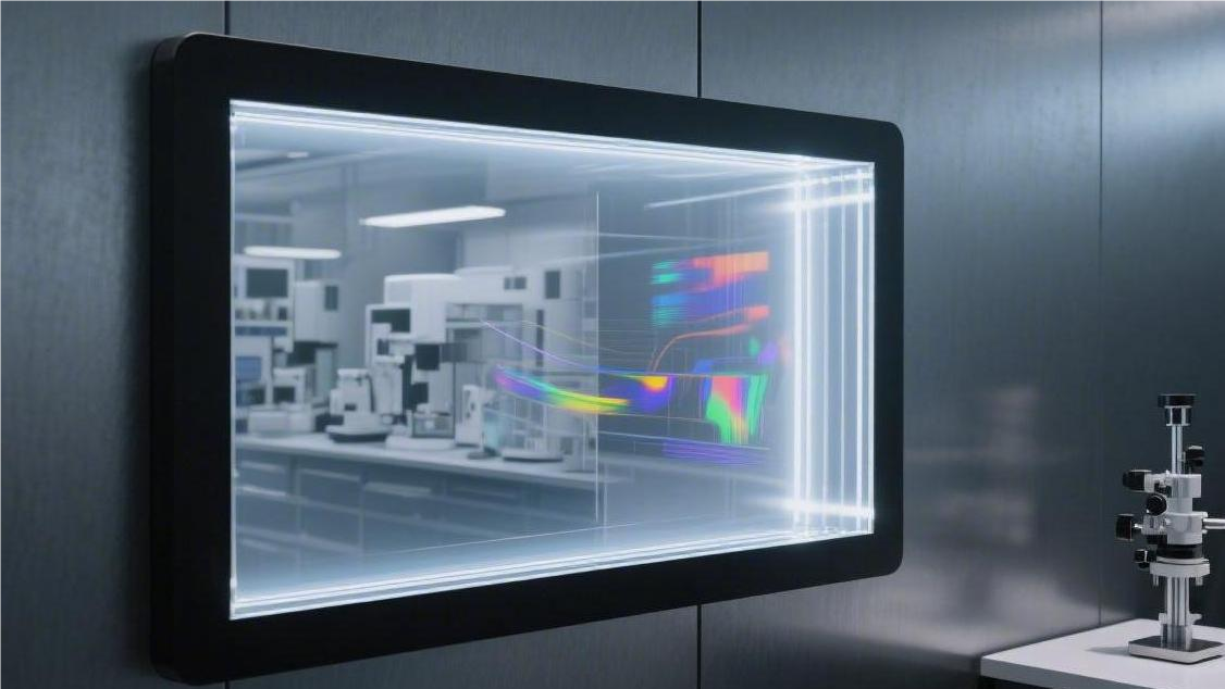
Industrial Maintenance Assistance
In automated factories across North America and Europe, transparent OLEDs are reconstructing the interaction logic of assembly lines and maintenance stations. This display substrate, merely 1.5 millimeters to 2.0 millimeters thick, uses a 38% physical transmittance rate to ensure technicians examining precise mechanical structures do not have to constantly switch focus between paper manuals and the physical object.
Relying on Oxide TFT driving technology, T-OLED can achieve a 120Hz native refresh rate. When processing sensor data streams above 60 frames per second, the visual delay between the screen-displayed 3D virtual guide lines and the real physical equipment is squeezed to under 10 milliseconds, eliminating screen tearing during dynamic observation.
When technicians face aviation engines or high-voltage switchgear comprising over 500 precision components, the T-OLED screen captures the machine's geometric features in real time via a 3D vision sensor array mounted on its back. Using spatial anchoring technology, the system precisely superimposes CAD original engineering drawings at 1920x1080 pixel clarity onto the surface of the corresponding physical parts.
The internal micro-lens array integrated into the panel can lock the focal length of the virtual image onto the observer's eyes. This optical solution allows superimposed 3D maintenance step text to remain sharp under a 600-nit peak brightness. Even if factory ambient lighting hits 2000 lux, text contrast can still be held at an industrial-grade standard of 150,000:1.
-
Real-time Bolt Preload Monitoring: The moment the wrench touches the bolt, the screen simultaneously displays the current torque value (unit: Nm) directly above it.
-
Internal Oil Pipeline Flow Simulation: Uses semi-transparent layers to display fluid velocity (e.g., 2.5m/s) and pressure fluctuations inside enclosed pipes.
-
Electrical Wiring Logic Enhancement: Marks complex wire harness loops with different colors, keeping positioning precision within a 0.5-millimeter error margin.
-
Concealed Fault Heat Map: Integrates infrared sensor data to directly mark abnormal overheating spots exceeding 85°C right onto the transparent glass.
-
Virtual Disassembly Guidance: Shows component removal paths next to the physical object at a 1:1 scale, slashing misoperation risks by over 30%.
-
Safety Exclusion Zone Boundaries: Projects red warning tapes at the edge of robotic arm operating trajectories, with a response time of just 0.1 milliseconds.
This highly efficient interaction relies on color accuracy provided by a 10-bit color depth. During complex circuit board troubleshooting, T-OLED can distinguish minute resistor color band differences thanks to a 100% NTSC wide color gamut. The system hovers detected voltage values (like 5.02V) right above the test point, keeping the operator's focal point steadily locked on the soldering area.
Targeting multi-layer circuit board diagnostics, the transparent screen supports deep occlusion culling algorithms. When the maintenance personnel adjust their viewing angle, the system updates the rendered view in real-time based on the 178-degree wide viewing angle characteristic. When viewed from the side, hidden internal routing paths still perfectly match the physical layout of the real soldering pads.
The surface of these T-OLEDs is coated with a 9H hardness nano silicon-carbon coating to resist corrosion from industrial cleaning agents. After 30,000 hours of continuous operation, brightness attenuation is controlled to within 5%, ensuring long-term industrial reliability.
Annotations drawn by remote experts on tablets are mapped to the on-site worker's transparent screen with millisecond latency via 5G industrial private networks, realizing cross-regional visual alignment collaboration.
-
Dynamic Annotation Sync: A specific valve circled by a remote expert automatically locks into position on the field screen.
-
Multi-dimensional Parameter Dashboard: Scrolls over 15 sets of operational data (like RPM, amplitude) continuously along the screen's edge.
-
Mandatory Operation Step Check: The technician must complete the current torque fastening action before the system releases the next command.
-
Anti-glare Coating Optimization: Drops external strong light reflection below 2%, ensuring clarity even under intense welding light.
-
Biometric Access Authorization: Only authorizes technicians with Level-4 qualifications to operate, verified through a transparent palm-print scanning module at the bottom of the screen.
Data indicates that by utilizing T-OLED for maintenance assistance, technicians have increased the First Time Fix Rate (FTFR) for complex electromechanical systems by approximately 22%.
Read more
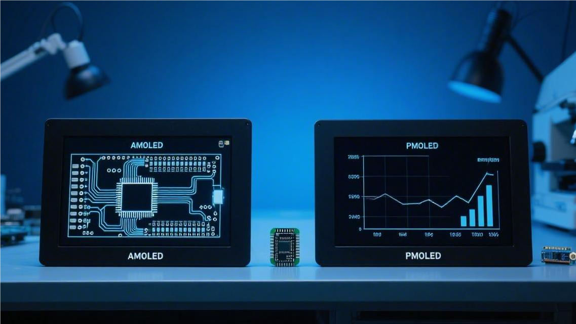
AMOLED utilizes a TFT array for active driving, where pixels are independently controlled, allowing sizes to exceed 100 inches. Although the cost is high, the picture quality is exquisite; PMOLED r...
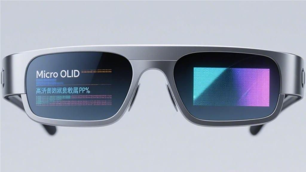
Micro OLED panels are the ideal choice for smart glasses. Their pixel density reaches 3000 to 4000 PPI, presenting high-definition vision without the screen door effect; The weight of a single scre...
Leave a comment
This site is protected by hCaptcha and the hCaptcha Privacy Policy and Terms of Service apply.