


What are the types of touch technology?
Major touch technologies include capacitive (smartphones, detecting 5+ fingers via body charge with ~10ms response) and resistive (ATMs, pressure-activated with 80% transmittance). Infrared variants suit large screens, sensing touches through blocked IR beams, while surface acoustic wave uses ultrasonic waves for precision.
Types of Touch Technologies by Technical Principle
While the global touchscreen market is projected to exceed $100 billion by 2028, the choice of technology is never one-size-fits-all. It hinges on a complex interplay of factors: a 5-finger multi-touch capability for a tablet, a >50 million-tap lifespan for an ATM, or the ability to function with a gloved hand in an industrial setting at -20°C. Understanding the core technical principles—each with distinct performance matrices for report rate (>120Hz for gaming vs. 60Hz for kiosks), touch accuracy (often within ±1mm), and optical clarity (with light transmission losses ranging from 5% to 15%)—is critical for selecting the optimal solution. This section breaks down the operational DNA of the five dominant touch technologies that power our interactive world.
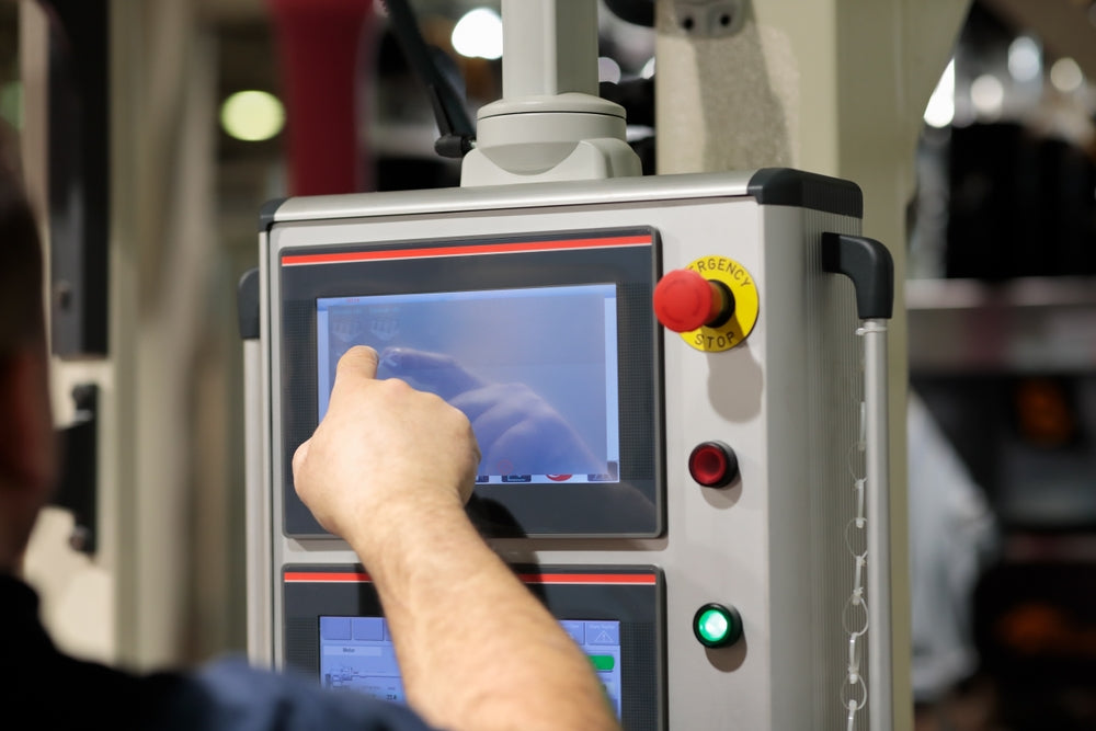
It comprises two flexible, conductive Indium Tin Oxide (ITO) layers separated by ~0.1mm microdots. Applying >5 grams of force causes the layers to contact, creating a voltage divider that pinpoints the touch with an accuracy of ±1.5mm. While highly durable and capable of accepting input from any object (stylus, glove), its ~75-85% optical transmittance and lower >8ms response time make it less ideal for high-speed applications. You'll typically find it in restaurant POS systems, industrial controls, and medical devices where a < $20 production cost and environmental robustness are more critical than dazzling visuals.
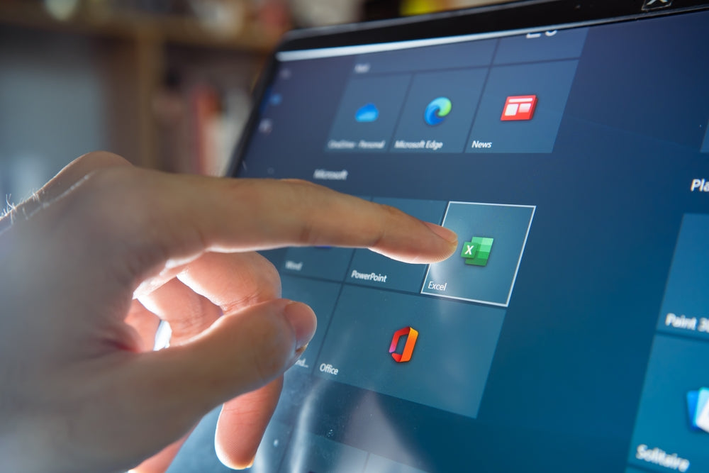
In stark contrast, capacitive technology, which dominates over 90% of the smartphone and tablet market, senses the electrical properties of the human body. It works by monitoring the distortion of a uniform electrostatic field. The more advanced Projected Capacitive (P-Cap) variant uses a matrix of micro-fine electrodes (often with a pitch of 4-6mm) etched onto a glass substrate. This allows for exceptional < 3ms response times, multi-touch support for up to 10 simultaneous contacts, and a "zero-pressure" touch that requires a mere < 1 gram of force. Its superior >90% light transmittance provides a brighter, sharper image. The main trade-off is its higher cost and sensitivity to environmental noise and moisture, though modern controllers with >200Hz scan rates effectively mitigate this.
For larger formats, Optical Touch and Surface Acoustic Wave (SAW) offer compelling advantages. Optical systems, using infrared (IR) LEDs with wavelengths of 850-940nm and sensors arrayed around the bezel, can scale to massive 100-inch+ displays without significant cost increases. They detect any opaque object that interrupts the light grid. SAW technology, which relies on high-frequency ~5MHz ultrasonic waves traveling across the glass, offers exceptional >95% image clarity as it requires no conductive layers. However, it is susceptible to contamination from dust and moisture, limiting its use in clean environments. Both technologies support robust multi-touch but have a lower frame rate of ~60Hz, making them less suitable for fast-paced interactions.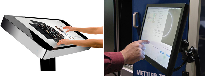
Integration of Touch Sensor with Display
A difference of just 0.5 millimeters in thickness or a 5% variation in optical transmittance can be the deciding factor in a smartphone's market competitiveness. The evolution from early, bulky add-on screens to today's sleek, seamless designs has been a relentless pursuit of thinner optical stack-ups, often aiming to reduce the air gap between layers to zero. This integration strategy influences everything from the Bill of Materials (BOM) cost, which can vary by 15-30% between methods, to the manufacturing yield rate, where more complex integrations can see >20% higher failure rates during production.
The classic GFF (Glass-Film-Film) structure, for instance, creates the sensor from two layers of ~0.125mm thick PET film with ITO patterning, laminated to a >0.5mm glass substrate. This builds a robust screen, but the multiple layers can result in a total thickness of over 1.5mm and a ~5-7% penalty in light transmittance, making the image appear slightly dimmer. A significant advancement here is the One Glass Solution (OGS), which etches the sensor electrodes directly onto the cover glass itself. This eliminates one glass layer, slimming the profile by ~0.3-0.5mm, boosting transmittance by ~3-5%, and improving touch response due to a shorter distance between the finger and the LCD pixels. However, OGS requires strengthening the chemically etched glass to maintain durability, adding ~10-15% to the processing cost.
For a truly integrated feel, On-Cell and In-Cell technologies are the industry standards for high-volume consumer electronics. On-Cell involves fabricating the transparent touch sensors, typically made from ITO with a sheet resistance of ~150-300 Ω/sq, directly onto the color filter glass of the LCD panel. This cleverly uses an existing layer, reducing the overall module thickness by another ~0.2mm compared to OGS. However, it requires precise manufacturing to avoid signal interference with the display drivers. The pinnacle of integration is In-Cell, where the touch sensor elements—often tiny <20µm capacitor electrodes—are embedded withinthe LCD cell itself, sharing the liquid crystal layer. This is the technology behind the sleek profile of most modern smartphones, allowing for module thicknesses of under 1.5mm and superior optical performance. The major challenge is "display noise;" the high-speed switching of the pixels (operating at frequencies of ~60-120Hz) creates significant electrical interference. This necessitates sophisticated controller chips that can sample the touch signal at speeds exceeding 200Hz and use complex algorithms to filter out the noise, increasing the IC cost by ~20%.
The core trade-off is clear: Add-on technologies offer design flexibility and lower development costs (a NRE of ~500k for In-Cell) but sacrifice thinness and optical performance. Integrated methods like In-Cell provide a superior user experience but come with higher manufacturing complexity and a significant risk of yield loss, especially on larger panels above 20 inches.
For specialized applications requiring extreme performance, Hybrid technology combines methods. A common approach is to embed a primary sensor inside the display (In-Cell) and add a fine-patterned metal mesh or ~5µm silver nanowire film on the cover glass. This external layer can boost the signal-to-noise ratio by >6dB, enabling features like palm rejection for stylus input or functioning with wet fingers. While this hybrid stack can add ~0.1mm and ~15% cost, it's a necessary solution for devices like high-end graphic tablets or automotive displays that demand >99.9% touch accuracy under all environmental conditions. The choice of integration is a calculated balance between performance specs, unit volume (with In-Cell only being cost-effective above ~1 million units), and the target selling price.
Touch Sensor Materials
The quest for alternatives is driven by the need for flexibility in foldable phones (requesting materials to withstand >200,000 bending cycles), scalability for 100-inch-plus interactive displays, and cost-reduction for mass-market devices. The ideal material would boast a sheet resistance of < 50 Ω/sq while maintaining >90% transmittance in the 550nm wavelength.
For over 30 years, Indium Tin Oxide (ITO) has been the industry benchmark, found in over 80% of touchscreens shipped in the last decade. Its popularity stems from an excellent balance of properties: typical sheet resistance values between 100-300 Ω/sq and optical transmittance consistently >85%. However, ITO has critical weaknesses. It's deposited in a high-temperature, high-vacuum sputtering process that consumes >60 minutes per batch and wastes up to 70% of the expensive indium target. Its ceramic nature makes it brittle; when deposited on flexible PET film, it can crack after just 1,000 bending cycles with a 2mm radius. Furthermore, its resistance increases significantly on panels larger than 15 inches, leading to signal latency and power drain.
Metal Mesh tackles the large-format challenge head-on. It uses a grid of ultrafine copper or silver wires, each typically 3-5 micrometers (µm) wide, spaced 200-500µm apart. This structure achieves remarkably low sheet resistance, often < 20 Ω/sq, even on displays measuring 85 inches diagonally. The trade-off is visibility; if the mesh pattern's pitch and line width aren't optimized, it can create subtle Moiré patterns when superimposed on the LCD's pixel array, especially with 4K resolutions (3840x2160). Newer photolithography techniques have reduced line widths to < 2µm, pushing optical transmittance to ~88% and minimizing visual artifacts, but this increases the production cost by 15-25% compared to standard ITO processes.
For flexible and foldable devices, Silver Nanowires (AgNW) are the leading contender. A random network of nanowires, each 20-50 nanometers (nm) in diameter and 10-25µm long, creates a conductive pathway that remains stable under repeated stress. AgNW-based sensors can achieve a sheet resistance of ~50 Ω/sq with >90% transmittance and withstand >200,000 bending cycles at a 1mm radius—a mandatory spec for foldable phones. The primary hurdle is long-term reliability under high temperature and humidity (85°C/85% RH), where silver can oxidize, causing resistance to drift by >10% over 1,000 hours. While Carbon Nanotubes (CNTs) offer phenomenal theoretical properties—a conductivity of 10^6 S/m and a transmittance of >99% for single-layer graphene—manufacturing challenges in creating uniform, defect-free sheets at a >95% yield rate have kept production volumes low and costs >10x higher than ITO, limiting them to niche military and aerospace applications for now.
|
Material |
Typical Sheet Resistance (Ω/sq) |
Optical Transmittance (%) |
Key Advantage |
Primary Limitation |
Best Application Size |
|---|---|---|---|---|---|
|
ITO (Sputtered) |
100 - 300 |
85 - 90 |
Proven reliability, high clarity |
Brittle, expensive, poor for large formats |
< 15 inches |
|
Silver Nanowire (AgNW) |
30 - 100 |
88 - 92 |
Excellent flexibility, high performance |
Potential oxidation, higher cost than ITO |
All sizes, especially flexible |
|
Metal Mesh |
5 - 30 |
85 - 89 |
Lowest resistance, great for large screens |
Risk of Moiré pattern visibility |
> 20 inches |
|
Carbon Nanotube (CNT) |
50 - 500 (highly variable) |
> 90 (theoretical) |
Theoretical best-in-class, chemical stability |
High manufacturing cost, uniformity issues |
R&D / Specialized |
A 30% reduction in sheet resistance (e.g., from 150 Ω/sq to 50 Ω/sq) can lower the controller's power draw by ~15% and improve the SNR by ~6dB, enabling more reliable touch in noisy environments. While ITO remains a viable solution for standard rigid displays under 15 inches, the industry's trajectory is clearly toward nano-based and metal mesh solutions to enable the next generation of large, flexible, and cost-effective touch interfaces.
Read more
The liquid crystal box is the core component of a liquid crystal display (LCD), and the display effect is mainly influenced by the liquid crystal box. The main parameters of the liquid crystal box...
Resistive touch tech uses two conductive layers—an ITO-coated glass top and a PET film bottom—separated by micro-spacers. Pressing bends the top layer to contact the bottom, altering resistance; co...
Leave a comment
This site is protected by hCaptcha and the hCaptcha Privacy Policy and Terms of Service apply.