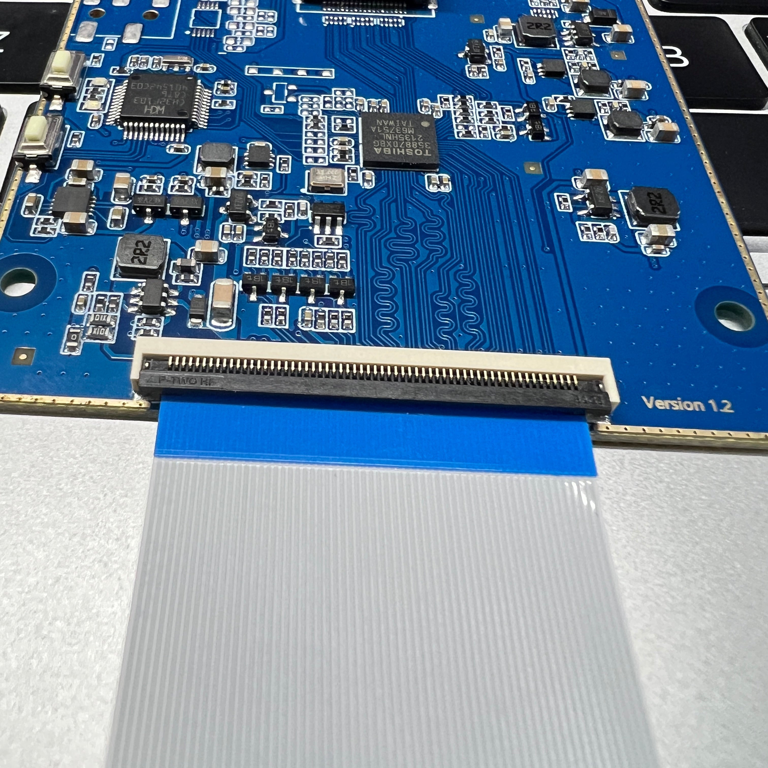
What is MIPI DSI (Display Serial Interface)?
MIPI DSI, a serial interface by MIPI Alliance, connects SoCs to displays in smartphones/tablets. It uses 1-4 data lanes (1.5Gbps/lane), maxing at 6Gbps total, slashing pin count while transmitting video/control signals.
Introduction to DSI
Every time you swipe through your phone's gallery or watch a 60-frames-per-second video, a sophisticated digital pipeline is working tirelessly behind the scenes. That pipeline is often built on MIPI DSI (Display Serial Interface), the de facto standard that has delivered pixels to over 15 billion mobile device displays. DSI isn't just a cable; it's a meticulously engineered protocol that solves a critical challenge: moving vast amounts of visual data from the application processor to the screen with extreme efficiency and minimal power drain. For a modern 1440p resolution display, a single frame contains over 5.6 million pixels. To refresh that at a smooth 60 Hz, the interface must handle a staggering 340 million pixels per second. DSI accomplishes this feat not with a wide, power-hungry parallel bus, but by using a sleek, high-speed serial interface that can reduce the pin count by over 80% compared to older RGB interfaces, saving crucial space and cost in compact devices.
You'll typically find a configuration with 1 clock lane and 1 to 4 data lanes. Each data lane in a common D-PHY implementation can achieve a data rate of up to 2.5 Gbps. This means a 4-lane DSI setup can deliver a total bandwidth of nearly 10 Gbps, which is more than enough for a 4K display at 60 Hz, even accounting for protocol overhead. This high-speed mode operates with a low 200 mV differential signal swing, which is a key factor in keeping electromagnetic interference (EMI) low and preventing noise from disrupting other phone components.
The system doesn't run at 10 Gbps continuously; that would drain the battery in minutes. Instead, it operates in two distinct states:
-
High-Speed (HS) Mode: This is the "sprint" mode. When the screen content changes—like during video playback or scrolling—the interface activates HS mode. The lanes switch from a low-power state to a high-frequency, low-voltage swing mode, blasting data for the duration of a frame transmission. For a typical 1.5-second screen transition, the HS mode might only be active for a few milliseconds to transfer the new image.
-
Low-Power (LP) Mode: This is the "standing" or "idle" mode. In between frame updates, or when the screen is static (like when you're reading text), the system drops into LP mode. In this state, the data rate plummets to less than 10 Mbps, but the power consumption drops even more dramatically—often to microwatts of power—which is over 99% lower than the active HS mode. This rapid switching is what allows your always-on display to show the time for hours while using less than 1% of the device's battery per hour.
Video Mode is like a constant livestream, where the processor continuously sends a stream of pixel data to the display. Command Mode, which is dominant in AMOLED displays used in most high-end phones, is more efficient. The processor sends a compressed image packet and a "draw here" command to a small memory buffer (frame buffer) on the display driver chip itself. For a static screen, this might only need to happen once, allowing the display's own hardware to refresh the pixels while the main processor and DSI link can stay in a low-power state for over 99% of the time, significantly extending battery life. -1.png?width=1800&height=900&name=Banner%20Images%20-%20MIPI%20(11)-1.png)
What are D-PHY and M-PHY?
Within the MIPI ecosystem, D-PHY and M-PHY are the two cornerstone physical interfaces that bring these protocols to life. Think of them as the underlying electrical engines, each designed for different performance and power envelopes. D-PHY, the established workhorse, has been instrumental in mobile devices for over a decade, handling the high-speed data for displays and cameras in billions of smartphones. It efficiently operates with a typical signal swing of 200 mV in High-Speed (HS) mode, achieving data rates up to 2.5 Gbps per lane with a commonly used 1.2 V I/O voltage. In contrast, M-PHY is the high-performance specialist, built for scalability and extreme bandwidth. Leveraging a more complex geared architecture with multiple gear types (Gear1, Gear2, etc.), a single lane of its latest version (v5.0) can burst at speeds up to 11.6 Gbps per lane, targeting advanced applications like 5G modems, automotive sensors, and high-resolution computational photography.
D-PHY employs a source-synchronous clocking scheme, where a dedicated Clock Lane (1 differential pair) accompanies one or more Data Lanes (each a differential pair). It toggles between two distinct modes: High-Speed (HS) mode for burst data transfer (> 80 Mbps per lane) and Low-Power (LP) mode for control commands (< 10 Mbps per lane). This duality allows a display, for instance, to receive a high-frame-rate video frame in HS mode and then instantly drop to LP mode to wait for the next frame, drastically saving power. A typical 4-lane D-PHY configuration for a 1080p display at 60 frames per second can sustain an aggregate bandwidth of nearly 10 Gbps while maintaining excellent power efficiency.
M-PHY, however, was engineered for a broader range of data traffic patterns, from bursty to continuous. Its most significant architectural difference is the use of embedded clocking with 8b/10b encoding, eliminating the need for a separate clock lane. This not only reduces pin count but also enables advanced power states like STALL and SLEEP, which offer faster entry/exit times compared to D-PHY's mode switching, cutting latency to as low as 1 microsecond. Where D-PHY is relatively static in its configuration, M-PHY is highly dynamic. Its data rate is defined by a combination of Gear and HS-Gear rates. For example, a Gear3 lane running at HS-Gear3 (HS-G3) can operate at 5.8 Gbps per lane, while doubling that to 11.6 Gbps requires only a shift to Gear4 (HS-G4). This scalability allows a single M-PHY IP block to serve multiple functions within a system-on-chip (SoC), from a low-power always-on sensor hub (using lower gears) to a massive data pipe for a multi-camera array (using higher gears).
The evolution from D-PHY to M-PHY reflects the industry's shift from monolithic data streams to complex, packetized traffic. M-PHY isn't just faster; it's a more intelligent transport layer designed for the heterogeneous integration found in modern connected devices.
Choosing between them boils down to a detailed analysis of the target application's requirements. The following table summarizes the key differentiators:
|
Parameter |
MIPI D-PHY |
MIPI M-PHY |
|---|---|---|
|
Primary Application |
Displays (DSI), Cameras (CSI) - constant stream |
Storage (UFS), DigRF (3G/4G/5G), Inter-chip (UniPro) - bursty traffic |
|
Clocking Scheme |
Source-Synchronous (dedicated clock lane) |
Embedded Clock (8b/10b encoding) |
|
Key Power States |
HS Mode (active), LP Mode (control) |
Multiple states: SLEEP, STALL, HIBERNATE (deeper power savings) |
|
Max Speed per Lane |
~2.5 Gbps (v1.2, widely implemented) |
~11.6 Gbps (v5.0, scalable per gear) |
|
I/O Voltage |
1.2 V (or 1.8 V for some older implementations) |
Lower swing, typically 0.4 V to 0.75 V for active signaling |
|
Lane Configuration |
1 Clock Lane + 1 to 4 Data Lanes |
1 to 8 symmetrical Data Lanes (no dedicated clock) |
|
System Complexity/Cost |
Lower complexity, highly optimized for mobile |
Higher complexity, enabling a wider range of high-performance systems |
In practice, D-PHY remains the dominant interface for displays and basic cameras due to its maturity, lower silicon cost, and optimized power profile for screen refresh cycles. However, M-PHY is increasingly critical for high-bandwidth, low-latency subsystems like Ultra-High-Definition video processing, augmented reality/virtual reality (AR/VR) headsets requiring massive data throughput, and next-generation storage solutions. The power efficiency of M-PHY in its SLEEP state can be an order of magnitude lower than D-PHY in LP mode, making it suitable for always-on applications.
The relationship between DSI and Physical Layer Interfaces
The seamless imagery on your smartphone display, whether a 120 Hz gaming session or a static always-on clock, relies on a critical partnership: the MIPI DSI protocol and its underlying physical layer (PHY). DSI acts as the sophisticated project manager, defining whatneeds to be communicated—organizing over 2.3 million pixels for a 1080p frame into efficient packets alongside timing and command instructions. However, without a robust delivery system, these instructions are meaningless. This is where the PHY comes in, acting as the electrical workhorse that defines howthis data is physically transmitted across the tiny printed circuit board (PCB) traces connecting the application processor to the display panel. The choice of PHY directly dictates the maximum achievable performance; a modern 4K display at 60 frames per second requires a staggering data rate of approximately 6.0 Gbps, which is impossible without a high-speed PHY like D-PHY or C-PHY.
The collaboration between DSI and the PHY is a finely tuned orchestration of digital commands and analog signaling. Here’s a detailed breakdown of how they interact:
-
Protocol and Physical Layer Handshake: The DSI protocol stack generates data packets. Before transmission, these packets are handed off to the PHY's parallel interface, which is typically 8 or 16 bits wide. The PHY's transmitter then serializes this data, converting it into a high-speed differential signal. For a D-PHY operating at 2.5 Gbps per lane, it takes the parallel data and streams it out serially at a rate 2500 million times per second. The voltage levels are critically low; a D-PHY uses a 200 mV differential swing in High-Speed (HS) mode to minimize electromagnetic interference (EMI) and power consumption, while the Low-Power (LP) mode uses a larger 1.2V single-ended swing for robust control signaling at speeds up to 10 Mbps.
-
Real-World Operational Workflow: Consider a smartphone displaying a 60 fps video. For each frame, the DSI protocol commands the PHY to enter HS mode. The PHY then transmits the pixel data in a continuous burst. Between frames, or when the screen content is static, DSI instructs the PHY to drop into LP mode. This transition, which can happen in nanoseconds, reduces the power draw on the interface to a trickle, often less than 5 mW, compared to the >50 mW consumed during active HS transmission. This dynamic power management, governed by the DSI protocol but executed by the PHY, is responsible for saving hundreds of milliwatt-hours of battery charge daily.
-
Error Handling and Signal Integrity: The physical layer is responsible for maintaining signal integrity across a >10 cm PCB trace, which is susceptible to noise, attenuation, and skew. While the DSI protocol includes error detection mechanisms like a 16-bit cyclic redundancy check (CRC) on its packets, the PHY must maintain a low bit error rate (BER), typically targeting an astonishing 1 error in 10^12 bits.
The choice of PHY fundamentally shapes the capabilities and limitations of a DSI implementation. The following table contrasts the two most common PHYs used with DSI today:
|
Feature |
D-PHY (The Established Workhorse) |
C-PHY (The Spectral Efficiency Expert) |
|---|---|---|
|
Key Differentiator |
Separate Clock + Data Lanes (1 Clock, 1-4 Data) |
3-phase symbol encoding on a 3-wire trio (no dedicated clock) |
|
Signaling |
Differential (HS mode) / Single-Ended (LP mode) |
Tri-level signaling on each wire (3 voltage levels per wire) |
|
Typical Speed per Lane |
2.5 Gbps/lane (v1.2) |
~5.7 Gsps (symbols/sec) per trio, yielding ~2.28 Gbps/wire or 6.84 Gbps/trio |
|
Pin Efficiency |
Lower. 4 Data Lanes + 1 Clock Lane = 9 signal wires. |
Higher. Two trios (6 wires) can outperform 4 lanes of D-PHY. |
|
Primary Use Case |
Dominant in >80% of mobile displays for over a decade. |
Gaining traction in high-resolution displays (4K+) where PCB space is constrained. |
|
Power Profile |
Simple two-mode (HS/LP) operation. |
More complex power states, but can be more efficient per transmitted bit. |
The bandwidth, power efficiency, and physical cost (pin count, PCB complexity) of the display subsystem are all direct consequences of the chosen PHY. While D-PHY has been the bedrock of the mobile industry, handling data volumes exceeding 50 terabits per hour in a typical user's day, the push for higher resolutions and lower power is driving adoption of more advanced PHYs like C-PHY.
Read more
HDMI interface is the most common interface of hardware equipment, including projector, TV, box, player and so on a variety of hardware devices, are necessary HDMI interface. The HDMI interface is ...
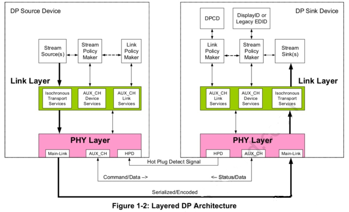
DisplayPort (DP) protocol is a high-speed serial interface standard for digital audio and video transmission, developed by VESA (Video Electronics Standards Association) DisplayPort was originally ...
Leave a comment
This site is protected by hCaptcha and the hCaptcha Privacy Policy and Terms of Service apply.