


COG LCD Technology | Advantages, Structure
COG (Chip-on-Glass) directly bonds the IC to the glass, thinning the module by more than 30% and refining the lead pitch to 40μm.
Its streamlined structure reduces costs by approximately 20% and significantly improves the stability of high-resolution screens, making it the preferred solution for slim devices such as modern smart wearables.
Advantages
COG packaging directly connects the IC to the glass substrate, eliminating the interposer carrier board and reducing module thickness to below 2 mm.
Utilizing ACF (Anisotropic Conductive Film) enables micron-level lead pitch bonding (approx. 30 microns), shortening signal transmission paths to the millimeter scale.
This solution reduces component weight by approximately 40% and supports high-density lead arrangements with over 1,000 channels.
By reducing discrete components, electrical reliability is improved, and in large-scale mass production, single-unit material costs can be reduced by approximately 15% to 25%.
Extreme Thinness and Lightweight Design
Traditional COB (Chip-on-Board) structures require a printed circuit board made of FR4 material with a thickness between 1.0 mm and 1.6 mm to carry the driver chip.
In contrast, COG involves hot-pressing the driver IC directly onto the glass substrate of the LCD panel.
Currently, mainstream display glass substrates have evolved from 0.7 mm in the early days to 0.5 mm or even 0.4 mm.
This direct bonding method reduces the physical height of the entire driver display layer by at least 60%.
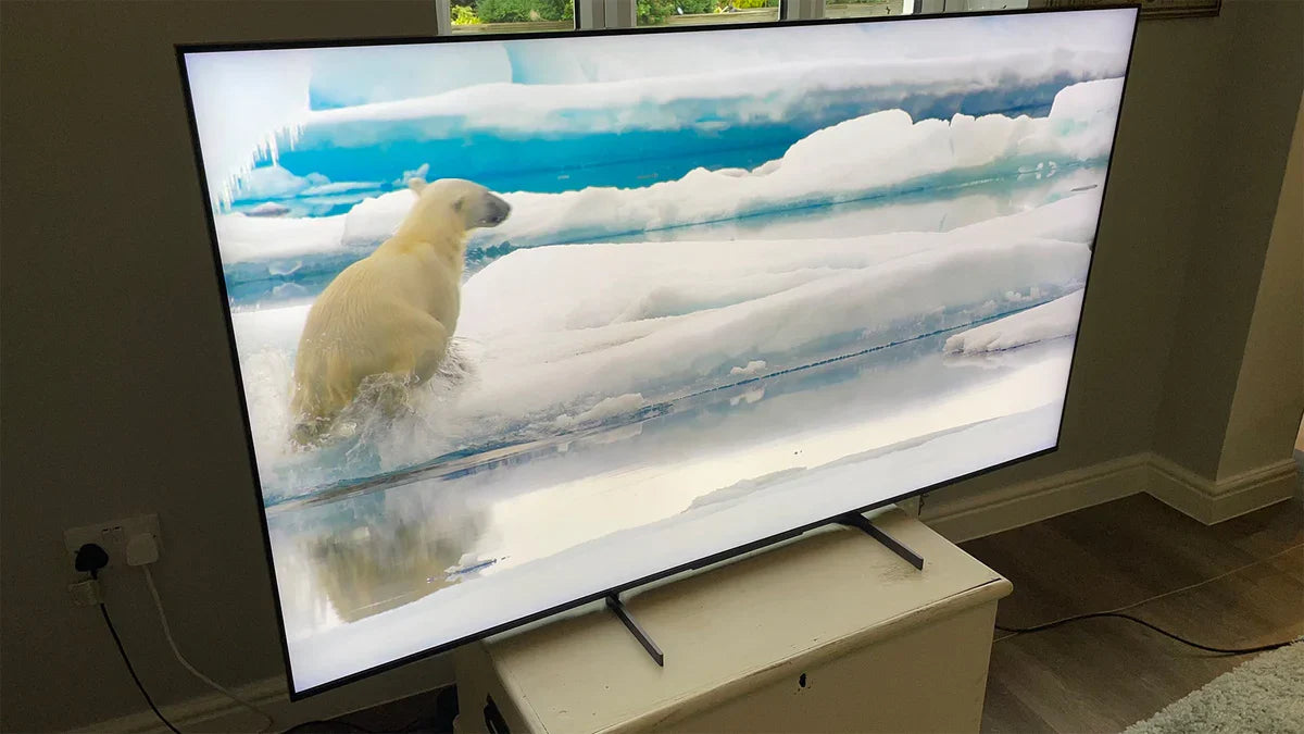
In smart wearable devices, where every micron of vertical space is precious, COG technology allows the total thickness of the screen module to be easily controlled within 2 mm, freeing up physical space for increased battery capacity or sensor stacking.
The driver chip itself undergoes a thinning process before packaging.
Through back-side wafer grinding technology, the thickness of the IC can be reduced from the original 700 microns to 200 to 300 microns.
These tiny chips are connected to the Indium Tin Oxide (ITO) electrodes on the glass via gold bumps with a height of only 10 to 15 microns.
The anisotropic conductive adhesive filled in between has a thickness that is almost negligible after pressing.
In early display designs, the non-display area at the bottom of the screen (commonly known as the "Chin" area) was often more than 10 mm wide due to the need for sufficient space to solder cables or fix circuit boards.
With the adoption of COG technology, because the lead pitch of the driver IC can achieve an ultra-high density of 30 to 40 microns, all driver circuits can be compactly arranged in a narrow strip at the edge of the glass.
Currently, the width of this non-display area can be reduced to between 1.5 mm and 3 mm, which directly contributes to the industrial design aesthetic of near-full screens.
On large automotive center consoles or handheld terminals, this narrow bezel design significantly increases the effective display area ratio.
The reduction in weight is equally objective. By removing the PCB, redundant pin connectors, and solder, the number of parts in the entire display module is significantly reduced.
Taking a 2.4-inch standard industrial display module as an example, the weight of a traditional packaged module might be around 15 grams, while the weight can be reduced to 8 to 9 grams by switching to the COG solution.
In overall system integration, COG modules present a completely flat physical surface because there are no protruding electronic components on the back.
This flatness allows the backlight module, light guide plate, and reflective sheet to be assembled directly against the back of the glass without the need to reserve buffer pads or air gaps to avoid electronic components.
This tight layered structure not only further compresses the Z-axis height of the entire machine but also improves optical penetration efficiency by eliminating air layers.
In high-performance tablet designs, this architecture, combined with 0.2 mm thick ultra-thin polarizers, allows the entire device to challenge the limit record of less than 5 mm thickness.
Because the chip is on the glass, the distance from the IC output to the pixel electrode is shortened to within 5 mm.
In contrast, traditional cable connection methods often have paths exceeding 20 mm.
A shorter path reduces the horizontal space occupied by routing and means there is no need to lay down large areas of metal interconnect layers on the glass surface, thereby keeping the substrate lightweight.
Due to the extremely strict spatial environment, aircraft instrument panels must integrate complex backlight, filter, and display layers within a limited depth.
The COG solution allows display components to be embedded into brackets like stickers by eliminating heavy FPC flexible connection strips.
This extreme space utilization allows designers to put larger resolution screens in the same instrument position without changing the physical structural layout of the aircraft.
Material Expenditure Streamlining
Traditional display modules usually require an FR4 rigid PCB or a large area of flexible circuit board as the base for the driver chip.
The procurement cost of such interposer carriers accounts for about 12% to 18% of the Bill of Materials (BOM) of the entire display module.
COG technology completely eliminates this extra circuit board and its supporting electronic components by directly bonding the driver IC to the liquid crystal glass substrate. This structural change directly reduces the material cost of a single module by approximately $0.15 to $0.50.
The connection method of the driver IC has also changed from expensive wire bonding or SMT processes to the more economical ACF (Anisotropic Conductive Film) hot-pressing process.
In traditional packaging, large amounts of solder paste, flux, and gold wires are required to ensure a stable connection between the chip and the circuit board, whereas the COG solution only requires the use of ACF tape with a width of approximately 1.5 mm to 2.5 mm.
Specific details of COG process material streamlining include:
- Circuit Carrier Elimination: The FR4 auxiliary circuit board with a thickness of 0.8 mm to 1.6 mm is removed, and the copper foil etching process on the board is also eliminated, reducing dependence on high-priced copper-clad laminates.
- Reduction in Connector Count: BTB interfaces or slot-type connectors used to connect the display screen to the mainboard in traditional structures are simplified. Since the driver IC is already integrated on the glass, the function of the FPC flexible board changes from "carrying the chip" to "signal transmission," and its number of layers can be reduced from 4 to 2 or even a single layer.
- Passive Component Integration: Modern COG driver chips reduce the need for external filter capacitors and current-limiting resistors through internal circuit optimization, usually saving the material expenditure of 5 to 8 SMD components around the display area.
- Packaging Material Savings: Compared to COF packaging, which requires expensive polyimide (PI) film as a substrate, COG directly utilizes existing glass substrate space, reducing the area of PI film used by more than 70%.
In the COB process, the PCB needs to go through multiple energy-consuming stages such as solder paste printing, high-speed placement, reflow soldering, and AOI inspection, each of which generates material loss and non-conforming repair costs.
The COG production line simplifies this into a single Gold Bump alignment and hot-press bonding.
The cycle time for the entire bonding process is typically controlled within 5 to 8 seconds.
This highly automated process reduces dependence on skilled technical workers, allowing the share of labor costs in total output value to drop from around 10% to near 4%.
By removing the thick PCB, the flatness of the back of the module is extremely high, and there is no longer a need to design complex slotted plastic frames or anti-static buffer pads to protect electronic components.
The thinning of the module thickness has increased the loading density of packaging boxes by 25% to 35%, meaning that more than 3,000 additional finished modules can be loaded within the same container volume.
The quantitative performance of this cost optimization in different application scenarios is as follows:
| Material Category | Traditional COB Cost | COG Solution Cost | Savings Magnitude |
|---|---|---|---|
| FPC Length | Approx. 50 mm to 80 mm | Approx. 20 mm to 30 mm | Approx. 60% |
| Solder / Gold Wire | Approx. 0.05 g/unit | 0 g | 100% |
| Protective Bracket | Custom injection molded parts required | Simple adhesive backing only | Approx. 45% |
| Substrate Components | 3 to 5 pieces | 1 to 2 pieces | Approx. 50% |
Since it is no longer necessary to purchase specific circuit boards and supporting passive components, companies can concentrate their procurement efforts on two major categories: liquid crystal glass raw materials and driver ICs.
This centralized procurement model increases bargaining power with upstream suppliers, usually resulting in an additional 3% to 5% price discount in bulk purchase agreements.
For developers of industrial equipment and automotive displays, the material streamlining brought about by COG is reflected not only in the reduction of initial procurement costs but also in the maintenance expenditures over the full life cycle.
Reducing separate connection structures reduces the risk of poor contact caused by vibration or high-low temperature cycles.
In automotive endurance tests from -40°C to 85°C, the unit failure probability of the COG structure is about 150 PPM lower than that of multi-component connection structures.
High-Frequency Signal Quality
Traditional packaging methods require signal relaying through flexible circuit boards or printed circuit boards, resulting in signal transmission paths often exceeding 20 mm to 50 mm.
In the COG structure, the gold bumps of the driver IC are connected to the ITO electrodes on the glass surface via anisotropic conductive film, shortening this physical distance to 2 mm or even less.
According to RF signal transmission theory, shortening the conductor length simultaneously reduces distributed inductance and capacitance.
Under the MIPI interface protocol with operating frequencies reaching 300 MHz to 1.2 GHz, this short-path characteristic significantly reduces signal reflection.
Experimental data shows that the signal rise-time jitter of the COG structure can be controlled within 50 picoseconds, ensuring that high-resolution images do not suffer from waveform distortion during fast refreshes.
The sheet resistance of ITO routing on glass substrates is typically maintained at 10 to 15 ohms per square.
Since it does not need to go through vias or complex pin switching, the continuity of signal impedance is guaranteed.
In high-speed display applications, impedance discontinuity leads to signal energy reflection at connections, generating interference waves.
The COG process uses gold bumps with a height of approximately 12 microns for vertical compression, and the contact resistance is typically below 5 ohms.
This low-impedance connection supports higher rates of current change, allowing the display screen to complete charge injection in a shorter cycle.
For high dynamic range display devices requiring a single-channel transmission rate of 1.5 Gbps, this structure maintains a wide "eye diagram" opening, significantly reducing the bit error rate.
The following table shows the quantitative differences in electrical signal characteristics between COG technology and traditional flexible connection solutions:
| Electrical Metric | COG (Chip-on-Glass) | COF/COB (Traditional) | Performance Improvement |
|---|---|---|---|
| Typical Path Length | 0.5 mm - 2.5 mm | 15 mm - 60 mm | Path shortened by approx. 90% |
| Distributed Capacitance | Approx. 0.3 pF - 0.8 pF | 2.0 pF - 5.0 pF | Reduced charge/discharge load |
| Signal Crosstalk Level | Below -40 dB | Approx. -25 dB to -30 dB | Reduced adjacent channel interference |
| Max Supported Clock | Above 1.0 GHz | Usually limited below 500 MHz | Adapts to UHD signal needs |
| Signal Latency | Approx. 10 - 30 ps | 100 - 300 ps | Improved response synchronization |
Because the glass substrate itself is an excellent insulating material with a dielectric constant between 5.0 and 7.0 and a very low loss tangent, it can effectively suppress the induction and coupling of electromagnetic waves between adjacent signal lines in high-frequency environments.
At the output of multi-channel driver ICs, the pin pitch might be only 30 microns.
On a polyimide film or FR4 substrate, such high-density wiring would produce severe mutual inductance effects, leading to signal crosstalk.
The physical properties of the glass substrate keep the induced electromotive force between adjacent lines at a very low level, and the signal integrity exhibits extremely high linearity during transmission.
In automotive display EMC testing, modules using COG packaging have radiated emission interference 10 to 15 dB lower than traditional structures, making it easier for display systems to pass strict aviation or automotive electronic interference standards.
The bonding area between the driver IC's gold bumps and the glass electrodes is typically between 1200 and 2500 square microns.
The number of conductive particles within a single connection point is usually designed to be 5 to 15.
"In display driver circuit design, for every millimeter of increase in the signal transmission path, the resulting impedance fluctuations cause non-negligible phase shifts in the high-frequency band. Adopting glass direct-connection technology essentially eliminates the energy loss caused by signals jumping between heterogeneous materials."
Because transmission losses are reduced, the charge pump inside the driver IC no longer needs to provide excessively high compensation voltage to offset line voltage drops.
In mobile devices, this means the dynamic power consumption of the display chip can be reduced by approximately 20%.
More stable waveforms also allow the timing controller (T-CON) to use more compact synchronization pulses, thereby optimizing the effective scanning time of each frame.
For displays supporting 120Hz or higher refresh rates, COG technology provides the necessary physical foundation to ensure that data signals can accurately drive the deflection of liquid crystal molecules within extremely short gate pulses.
The thermal stability of the glass material also provides an implicit guarantee for signal quality.
The linear expansion coefficient of glass is approximately 3.7 to 4.5 x 10⁻⁶ /°C, which is far lower than that of plastic substrates.
As temperature increases during long-term device operation, the geometric dimensions of the metal traces on the glass remain highly stable.
This thermal stability ensures that high-frequency impedance fluctuates very little over a wide temperature range of -40°C to 85°C.
Structure
The COG structure eliminates IC packaging by directly attaching the Bare Die to the glass substrate.
The connection interface relies on ACF (Anisotropic Conductive Film), which is filled with conductive gold spheres with a diameter of 3 to 5 microns.
The Gold Bumps of the driver IC (approx. 10 to 15 microns high) make physical contact with the ITO transparent electrodes on the glass through hot-pressing.
This design allows the pin pitch to shrink below 30 microns and the overall module thickness to be reduced by about 2 mm compared to traditional methods, significantly reducing the resistance and inductance of the signal loop.
Physical Composition of Components
As the basic carrier of the entire module, the glass substrate is usually chosen from alkali-free silicate glass with a thickness between 0.4 mm and 0.7 mm.
This material has a Coefficient of Thermal Expansion (CTE) of approximately 3.7 to 3.8 ppm/°C, ensuring no significant deformation during the high-temperature bonding process.
A layer of Indium Tin Oxide (ITO) conductive layer is covered on the glass surface via sputtering, with a thickness typically maintained at 100 to 150 nm.
This extremely thin transparent conductive film has a resistivity of 10 to 15 ohms per square, and its main role is to establish a path for signals from the chip to the liquid crystal pixels.
In actual layout, a strip with a width of 2 to 3 mm is reserved at the edge of the glass as the Bonding Area, where all signal exchanges are completed.
"In a COG structure, the driver IC exists in the form of a Bare Die, eliminating traditional plastic encapsulation and lead frames."
This bare die is cut from a silicon wafer, with a length typically ranging from 10 to 25 mm, a width as narrow as 1 to 1.8 mm, and a thickness of only 250 to 300 microns after the thinning process.
Gold bumps with a height of 10 to 15 microns are grown on the input and output pads of the chip via electroplating.
The Vickers hardness of the gold bumps is usually set between 50 and 80 Hv, ensuring they can stably compress the conductive particles during hot-press bonding.
The arrangement pitch of the gold bumps is very tight, usually around 20 to 30 microns, allowing a single chip to accommodate more than 1,000 pins to support high-resolution screen data processing.
"ACF (Anisotropic Conductive Film) acts as both an adhesive and an electrical bridge; its microscopic internal structure ensures vertical conduction without horizontal short circuits."
ACF film is mainly composed of an epoxy resin matrix and conductive particles uniformly distributed within.
These particles have a diameter generally between 3 and 5 microns and usually feature a plastic sphere core with gold or nickel plating.
Their density is precisely controlled at 3,000 to 5,000 per mm².
At room temperature, this material is non-conductive, but when subjected to high temperatures of 180 to 210°C and pressures of 60 to 100 MPa, the particles trapped between the gold bumps and the ITO are flattened into ellipsoids.
This physical deformation increases the contact area, reducing the contact resistance of a single point to below 1 ohm.
The Flexible Printed Circuit (FPC) serves as the relay station for external signals entering the glass substrate.
Its main material is a polyimide (PI) film with a thickness of 12.5 or 25 microns.
A layer of electrolytic or rolled copper foil with a thickness of 18 or 35 microns is attached to the PI film to form complex circuit traces.
To prevent oxidation and improve soldering performance, the surface of the FPC contact fingers is nickel-gold plated.
The connection between the FPC and the glass substrate also uses the ACF pressing process, known as OLB (Outer Lead Bonding).
In practice, the bonding pitch on the FPC side is typically between 0.1 and 0.2 mm, which is much larger than the pin density on the chip side to reduce assembly precision requirements and improve yield.
"To prevent environmental moisture and impurities from corroding the micron-level connection points, the structure also includes a sealed protective layer."
After the chip is attached, technicians apply glue to the four edges of the chip using a material called Silicon Resin or epoxy resin for edge sealing.
This glue layer's thickness is controlled at 50 to 100 microns, isolating air moisture and preventing open circuits caused by electrochemical migration of the ITO film under power.
Since the display screen generates heat during operation, this encapsulated structure must be able to withstand thermal cycle tests from -40 to 85°C without delamination or increased contact resistance.
Polarizers are attached to both sides of the glass substrate, with each layer approximately 0.1 mm to 0.2 mm thick.
They are composed of multiple layers of polymer films, including a TAC layer for mechanical support and a PVA layer for light polarization.
In the overall space calculation of the COG module, the total thickness from the top of the backlight module to the top polarizer is often compressed to within 1.5 mm.
Due to the removal of redundant packaging materials, the signal transmission path is shortened from the original centimeter scale to the millimeter scale, reducing the signal transmission inductance by 40% to 60% and significantly improving performance in EMC tests.
Micron-Level Connection Surface
In the physical construction of COG technology, the micron-level connection surface is the boundary where the driver chip and the glass substrate achieve signal interaction, with its thickness typically compressed between 10 and 15 microns.
Within this tiny space, the establishment of the conductive path relies entirely on mechanical extrusion and electrical contact between the gold bumps, the conductive particles in the ACF, and the ITO electrodes on the glass.
These particles typically use a polymer core coated with a nickel layer of approximately 0.1 microns and a gold layer of approximately 0.05 microns.
The average diameter of the particles is distributed between 3.2 and 4.8 microns, with a standard deviation usually required to be less than 0.2 microns to ensure uniform force on each contact point during hot-pressing.
In each square millimeter of ACF film, the particle density is maintained at 3,500 to 4,500.
The height error of the bumps (coplanarity) must be controlled within 2 microns.
If heights are inconsistent, pressure will concentrate on higher bumps, leaving particles under lower bumps uncompressed and causing abnormally high contact resistance.
Currently, mainstream pin pitch has reached 20 microns, with corresponding gold bump widths of only 8 to 12 microns.
This extremely high wiring density requires the alignment precision of bonding equipment to reach within ±3 microns, as any tiny offset will reduce the effective contact area.
- Deformation Rate Control: During hot-pressing, the diameter deformation of conductive particles must be maintained between 30% and 50%.
- Pressure Distribution: The pressure on the connection surface is typically set at 70 to 90 MPa, ensured by calibrating the flatness of the hot-pressing head.
- Temperature Gradient: The temperature of the connection surface rises rapidly to 190–210°C within 5 to 10 seconds to induce epoxy resin curing.
- Cohesion Performance: The peel strength of the cured ACF resin must exceed 400 g/cm to resist external thermal stress.
The hot-press bonding process directly determines the microscopic morphology of the connection surface.
When the thermode descends and applies pressure, the physical changes are intense.
Under this pressure, the spherical conductive particles are flattened into disc shapes, breaking the insulation coating on the particle surface and enabling physical metal contact between the gold layer, the ITO electrode, and the chip bump.
In an ideal state, the connection resistance of a single pin is usually between 0.2 and 0.8 ohms.
If pressure is insufficient and the particle deformation is less than 20%, contact resistance will jump to over 10 ohms, causing signal distortion.
Conversely, if excessive pressure causes particles to rupture and expose the polymer core, conductivity will also drop.
Additionally, the insulation resistance between adjacent pins must be greater than 100 MΩ, requiring the ACF resin to have excellent fluidity during curing to push excess particles into non-charged gap areas.
During hot-pressing, if the gold bump hardness exceeds 80 Hv, it may cause micro-cracks in the ITO film below, which can evolve into electrochemical corrosion in long-term humid environments.
Therefore, material matching requires a reasonable hardness gradient between the chip bumps, conductive particles, and glass electrodes.
- Thermal Shock Resistance: The connection surface must withstand 500 cycles between -40°C and 85°C with resistance fluctuations under 20%.
- HTHH Stability: After 1,000 hours at 85°C and 85% RH, connection points should not show oxidation or delamination.
- Current Carrying Capacity: A single connection point must support a steady-state current of 10 to 50 mA without local thermal degradation.
- Corrosion Barrier: The sealing thickness at the chip edge must reach 50 to 100 microns to isolate the interface from water vapor erosion.
Spatial Dimension Quantization
Vertical Height Physical Performance
Traditional packaging methods often exceed 2 mm in vertical height due to lead frames or independent PCB carriers, whereas COG drastically compresses this value.
Glass substrates are typically chosen in 0.5 mm or 0.7 mm specifications.
Before the bonding process, the driver IC undergoes wafer thinning, reducing its thickness to between 250 and 300 microns.
When the chip is pressed to the glass surface through an ACF layer only 10 to 20 microns thick, the total height from the top of the chip to the bottom of the glass typically does not exceed 0.85 mm.
In mobile device design, this compression releases valuable internal stacking space, allowing battery compartments to increase in volume by about 5% to 10%.
Because redundant packaging shells are removed, the height travel of signals from the chip output to the liquid crystal layer is shortened by 70%, significantly reducing parasitic capacitance and keeping signal loss under high-frequency operation at an extremely low level within 0.5 dB.
| Component Name | Thickness (mm) | Space Occupancy (Ref) |
|---|---|---|
| Glass Substrate | 0.4 - 0.7 | Approx. 60% |
| Driver IC (Post-thinning) | 0.2 - 0.3 | Approx. 30% |
| ACF Bonding Layer | 0.01 - 0.02 | Approx. 2% |
| Polarizer (incl. adhesive) | 0.12 - 0.15 | Approx. 8% |
Border Area Physical Footprint
In a COG structure, this area is known as the Bonding Area.
Since the driver IC is attached horizontally as a long strip to the edge of the glass, the "Dead Zone" is greatly optimized.
The width of the driver IC is typically designed between 1.0 and 1.8 mm.
To ensure space for ACF overflow and sealant application, a margin of 0.3 to 0.5 mm is usually reserved between the chip edge and the glass cut line.
This means a complete COG bonding zone width can be controlled within 2.0 to 2.5 mm.
In contrast, traditional packaging techniques require over 5 to 7 mm of border width to accommodate cable bend radii and external PCB interfaces.
In common 18:9 or 20:9 screen ratios, for every 1 mm the bottom border is reduced, the visible screen area increases by about 1.5%.
In automotive dashboards, this compact border structure allows modules to embed larger display units into narrow center console spaces without extra mechanical brackets for heavy external circuitry.
| Screen Size (Inches) | Typical Bottom Border (COG) | Typical Bottom Border (COB) | Reduction Ratio |
|---|---|---|---|
| 2.4" (Industrial) | 1.8 mm | 5.5 mm | 67% |
| 6.0" (Smartphone) | 2.2 mm | 7.0 mm | 68% |
| 12.3" (Automotive) | 3.5 mm | 10.0 mm | 65% |
Microscopic Circuit Distribution Parameters
The pin pitch between the driver IC and the glass electrode is a data indicator of the technology's advancement.
Currently, the pin pitch for high-resolution screens is typically between 20 and 35 microns.
Under such fine spacing, the line width and line space are usually set to 10 microns / 10 microns.
To ensure smooth current conduction, the ITO electrode thickness on the glass is maintained at 1200 to 1500 Å.
Each gold bump has a physical area of approximately 1000 to 1500 square microns and must achieve an alignment precision within ±3 microns relative to the ITO electrode.
This high-density distribution allows a single chip to drive over 1080 or 2160 data lines.
In a 4K resolution smart screen, the number of drive pins can even exceed 3,000.
If old wire-bonding methods were used, these pins would occupy over 100 mm in length, whereas COG technology utilizes micron-level pitch to compress all connection points into a narrow strip less than 30 mm long.
"On a 500 PPI display, the width of each sub-pixel is only 15 to 18 microns, requiring the output traces of the COG bonding area to physically match the pixel pitch."
Because the CTE of the glass substrate differs from the silicon chip by about 1 to 2 ppm, over a chip length of 20 mm, every 50°C temperature rise will produce a thermal displacement of about 1 to 2 microns at the edge pins.
Therefore, spatial dimension quantization includes tolerance design for thermal dynamic displacement.
Design specs usually require gold bumps to be 4 to 6 microns wider than the ITO electrodes to compensate for processing errors and thermal expansion, ensuring that at least 5 to 10 conductive particles are captured per pad in any environment.
Module Volume Comparison Quantization
From a system integration perspective, the volume reduction data brought by COG is significant.
In a 5-inch display module, removing the external driver board and bulky cables can reduce the total weight of the module by approximately 15 to 20 grams.
Since the chip is attached directly to the glass, the drive current does not need to flow through centimeters of FPC copper foil.
This path shortening reduces line internal resistance by about 3 to 5 ohms.
In a full-brightness state, this structural optimization can reduce system power consumption by about 50 to 100 milliwatts.
For 24-hour industrial control equipment, this results in lower heat generation and longer lifespans for electronic components.
This extreme space utilization represents a form of structural purity.
It solidifies complex semiconductor driving directly onto the display carrier, eliminating all intermediate mechanical connection stages.
Within a spatial range of 1.5 mm thickness, all physical connections from raw image data input to liquid crystal photoelectric conversion are completed.
Weiterlesen
Micro OLED is a silicon-based OLED technology with a pixel density exceeding 3000 PPI and a brightness of several thousand nits. It is small in size, has low power consumption, and offers extremely...
OLED holds an advantage in high-performance visual interaction with an ultra-high contrast ratio of >10,000:1 and an ultra-fast response time of <1ms, while LCD remains the preferred choice f...
Hinterlasse einen Kommentar
Diese Website ist durch hCaptcha geschützt und es gelten die allgemeinen Geschäftsbedingungen und Datenschutzbestimmungen von hCaptcha.