



The Guide to Micro OLED | Technology, Features & AR/VR Applications
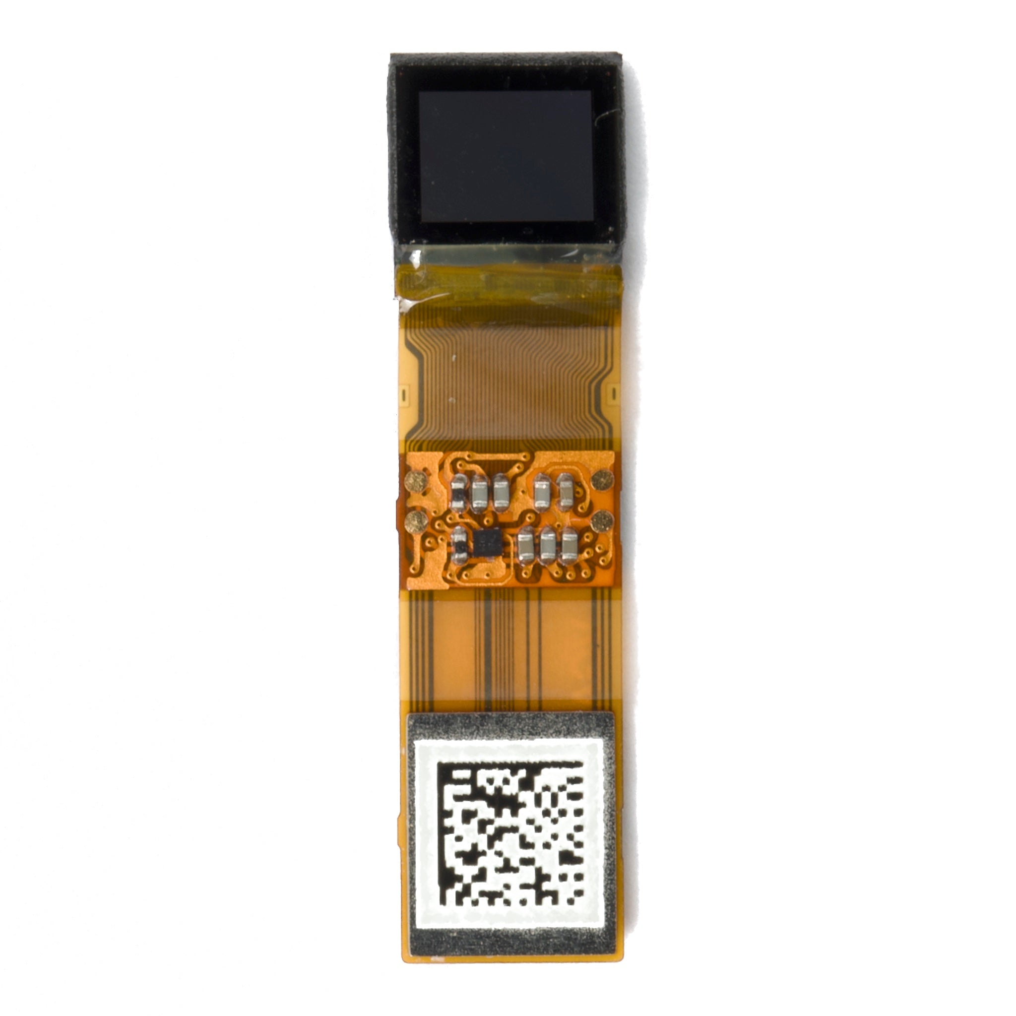
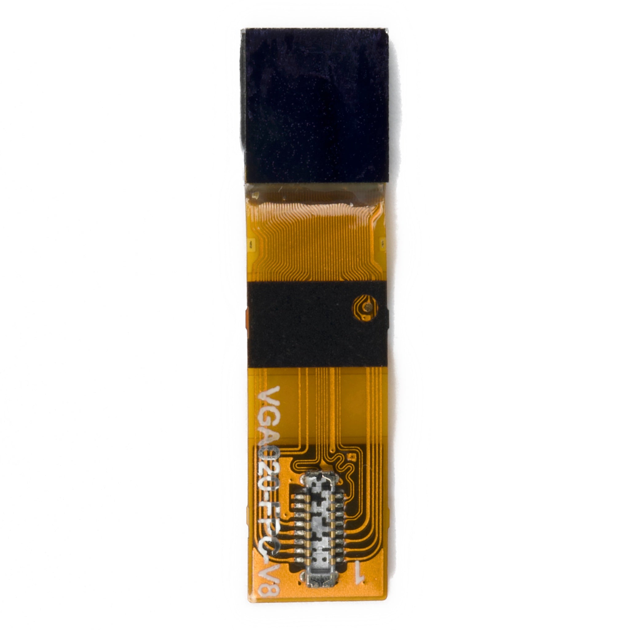
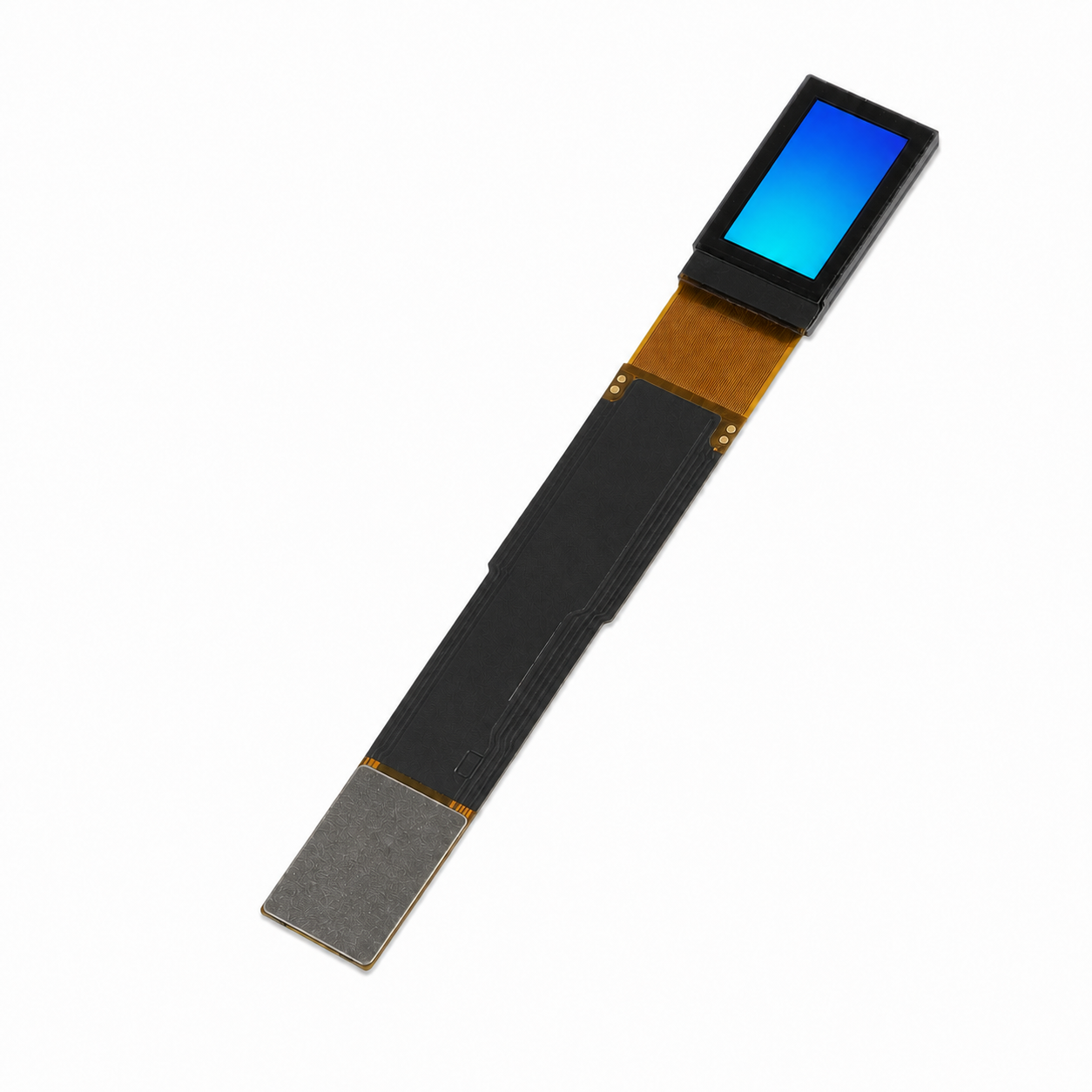
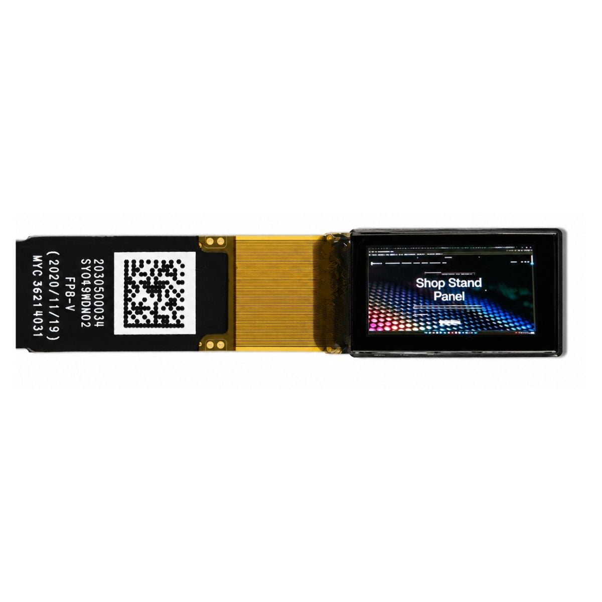
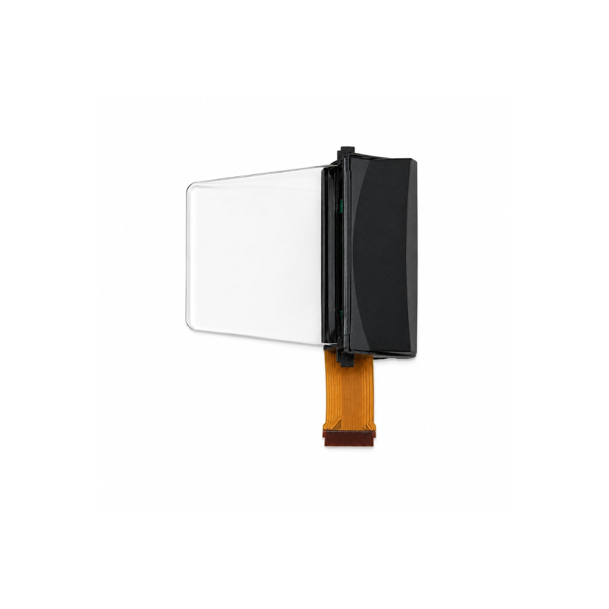
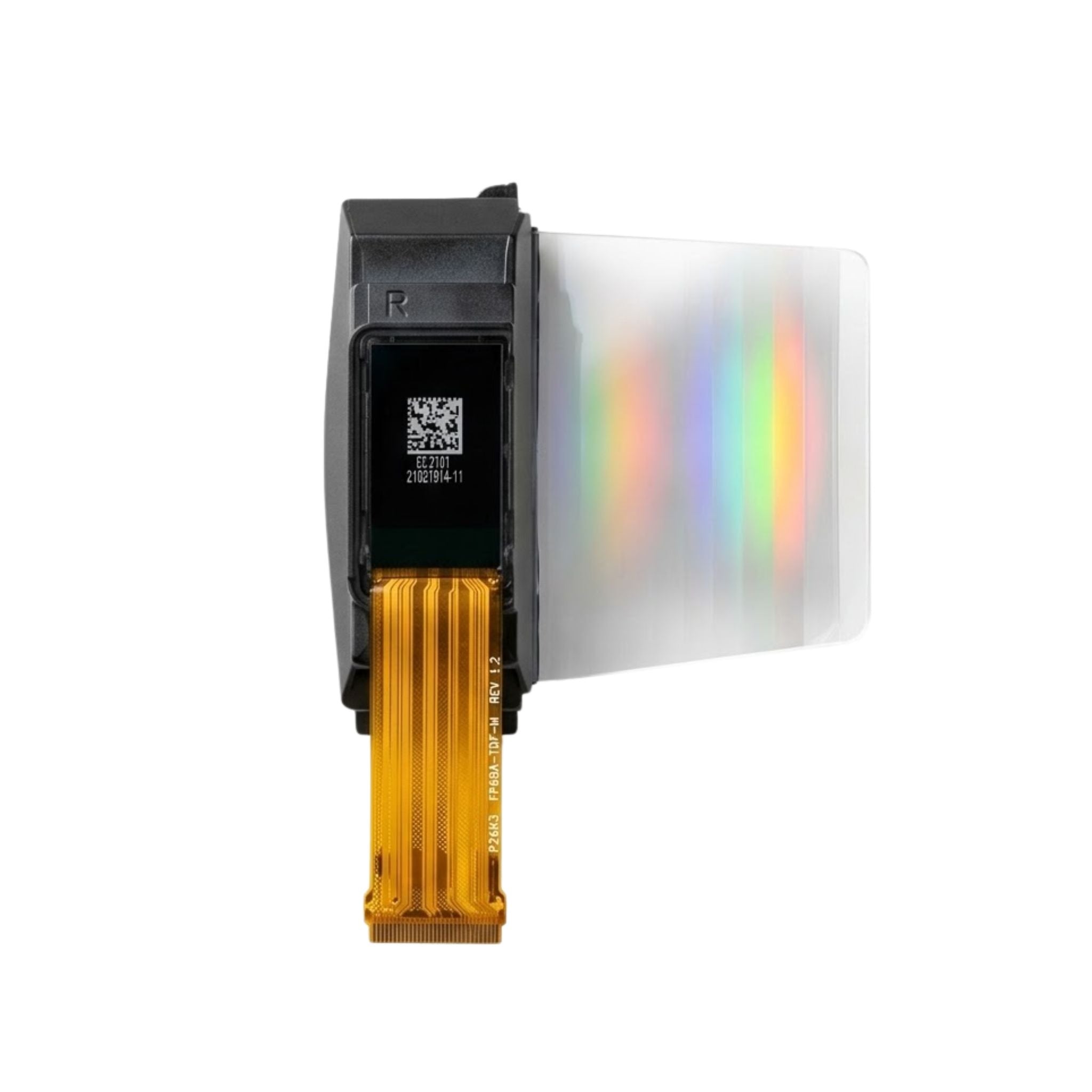
Micro OLED is an OLED display built on a single-crystal silicon CMOS backplane instead of on glass. That one substitution explains the rest of the technology: pixel densities in the thousands per inch, switching in microseconds, a die smaller than a postage stamp, and a cost to match. This guide covers how the panels are built, which specifications predict performance, and where the premium is worth paying.
Silicon backplane
On a glass panel the pixel switches are thin-film transistors deposited at temperatures the substrate can survive, and their carrier mobility limits how small a driver circuit can be. A micro OLED wafer is processed in a CMOS foundry instead, so the drive circuitry is part of the silicon. Timing, digital-to-analog conversion and per-pixel current control sit on the same die as the pixel array, which removes hundreds of interconnects between a separate driver chip and the panel.
Pitch follows from that integration. A 0.7-inch panel with 1920 by 1080 pixels works out to roughly 3,100 pixels per inch, so each pixel driver has to fit inside a cell a few micrometres across. Because the transistor sits underneath the emitting area rather than beside it, the panel can be built in a top-emission layout and keep a high aperture ratio at those dimensions. Pitch figures vary by generation and supplier, so treat one number as a snapshot.
White emitter and colour filters
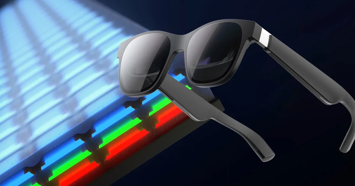
Most shipping micro OLEDs do not pattern red, green and blue emitters side by side. They deposit a white OLED stack, often two or three emitting units joined by charge generation layers, and then define colour with photolithographic filters above it. The reason is practical: fine-metal-mask evaporation, the standard route for phone OLEDs, struggles to hold alignment at micrometre pitches, while colour filters are made with the same lithography as the backplane. The device physics behind those stacked structures has been reviewed at length in the display literature[2].
The trade has a price. A colour filter absorbs a large share of the light passing through it, so a white stack has to run bright to deliver a modest white point at the eye. Tandem stacks partly answer this by connecting emitting units in series: for a given current the structure produces more photons per unit area, which lowers current density and slows the degradation that current density drives.
Brightness at the eye
A panel nit figure is not a headset nit figure. Between the panel and the pupil sit a combiner, a waveguide or a pancake lens, and every stage loses light. A diffractive waveguide delivers only a fraction of the panel output into the eye box, and a pancake cavity loses light at the partial reflector on each pass. The number that predicts outdoor usability is luminance measured at the eye position with the final optics fitted.
Micro-lens arrays are one lever. Hemispherical lenses aligned to each sub-pixel redirect light that would otherwise be trapped by total internal reflection at the organic-to-air interface, raising extraction efficiency and narrowing the emission cone, which helps when the optics accept a limited angular range. Specify the measurement condition as well: an on-axis reading in a dark room says nothing about a sunlit street.

Density and comfort
Angular resolution in pixels per degree predicts comfort better than pixels per inch. Foveal acuity resolves about one arcminute, which corresponds to roughly 60 pixels per degree; below that users can pick out structure in the image, above it most cannot at a normal gaze. Pixels per degree is panel resolution divided by field of view, so the same panel looks coarser in a wide-FOV headset and finer behind a narrow-FOV optic.
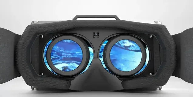
This is why density matters more in VR than in a viewfinder. A display that looks flawless at a 30-degree field can show visible screen structure at 100 degrees. It also explains why micro OLED displaced reflective technologies in near-eye products: liquid-crystal-on-silicon could reach the size, but not the contrast or the switching speed.
Response and motion
Emission itself is fast. An OLED pixel reaches its commanded brightness in microseconds because the process is carrier recombination in a thin film, not the physical rotation of liquid crystal molecules. That removes the smearing a slow LC cell adds to moving content.
System latency is a different budget. Motion-to-photon latency includes sensor sampling, pose prediction, rendering and scan-out, and in a headset those terms dominate. A fast panel buys time for the rest of the pipeline rather than eliminating delay by itself. Low persistence and black-frame insertion then cut retinal smear during head turns, which is where a fast emitter earns its keep.
Dimming deserves attention. Many modules vary brightness by pulse-width modulation, and others use analog current control or a hybrid of the two. At short duty cycles PWM can produce flicker or phantom contours in peripheral vision, so ask for the dimming scheme and the minimum pulse conditions instead of accepting a headline dimming range.
Contrast and flare
A pixel that is switched off emits nothing, so the panel's own black level is effectively zero and native contrast is limited by the driver's ability to hold a dark state, not by a backlight. System contrast is another matter. Every optical surface in the path reflects some ambient light back to the eye, and that flare lifts the black level the user actually sees.
Two consequences follow. Contrast claims should state whether they were measured on the bare panel or through the optics, and in what illumination. ISO 9241-307 defines how luminance and contrast are measured on electronic displays[1]. Second, anti-reflection treatment on the combiner often improves perceived contrast more than another hundred nits of panel output.
Lifetime and heat
Blue emitters age faster than red and green, and ageing accelerates with current density and temperature. Tandem structures reduce current density at a given brightness, silicon conducts heat better than glass so warmth spreads into the package instead of sitting in the organic stack, and many backplanes trim drive current as the die heats. Together these extend usable life; none of them removes the trade between brightness and hours.
Ask for lifetime at the brightness you intend to run, with duty cycle and ambient temperature stated. A figure quoted at half the target brightness is not comparable, and a figure quoted at room temperature says little about a sealed headset.
Where it fits
Near-eye display is the natural home. VR headsets use the density for wide fields of view; AR glasses use the size and contrast for see-through combiners, at the cost of pushing brightness hard to survive waveguide loss. Electronic viewfinders use the response and contrast in a small package. Surgical and industrial head-mounted systems use all three, plus the ability to render a true black overlay that does not glow over the real scene.
For panel options, browse the micro OLED collection and the AR and VR display collection. Where a small self-emissive panel is enough without silicon-level density, OLED modules cover the lower-density end of the range.
Selection checklist
Five questions separate a usable part from a datasheet. What is the luminance at the eye with the intended optics, measured in the intended ambient light? What is the resolution in pixels per degree at the target field of view? Which interface does the backplane expose, and what lane count and clock does it need? What is the power draw at representative content rather than at full white? And what are the operating and storage limits for the module, not just for the die?
Add two for production: how the supplier specifies brightness and colour uniformity across a wafer, and what happens to panels that fail inside the warranty period. Wafer test catches most defects, but optics assembly is where marginal parts usually surface.
None of these questions has one right answer. They have answers that suit an optical design, which is why a module specified against a headset outperforms a module specified against a datasheet.
References
- ISO 9241-307:2008 — Ergonomics of human-system interaction — Part 307: Analysis and compliance test methods for electronic visual displays. International Organization for Standardization. https://www.iso.org/standard/40102.html
- Hilsum, C. (2010). Flat-panel electronic displays: a triumph of physics, chemistry and engineering. Philosophical Transactions of the Royal Society A, 368(1914), 1027–1082. https://doi.org/10.1098/rsta.2009.0247
Weiterlesen
Micro OLED features 3000+ PPI and 5000 nit brightness, completely eliminating the screen-door effect; The 0.01 ms ultra-fast response time solves motion.
COG (Chip-on-Glass) directly bonds the IC to the glass, thinning the module by more than 30% and refining the lead pitch to 40μm. Its streamlined.
Hinterlasse einen Kommentar
Diese Website ist durch hCaptcha geschützt und es gelten die allgemeinen Geschäftsbedingungen und Datenschutzbestimmungen von hCaptcha.