


How Does NexPCB Help With XR Displays
NexPCB supports XR displays by delivering tailored PCB solutions, including 12-layer HDI boards with ±25μm micro-via precision to fit compact headset designs, enabling seamless integration of display drivers and sensors; their 99% yield rate for flex-rigid circuits also ensures stable.
12-Layer HDI Boards for Compact XR
NexPCB’s 12-layer HDI boards solve XR’s tight-space dilemma: they pack display drivers, motion sensors, and wireless modules into a 0.8mm-thick stack using ±25μm micro-vias, slashing design time by 30% for clients like AR glasses maker Vuzix. This density supports 4K-per-eye rendering without bulking up headsets,critical when every 0.1mm matters for comfort.
XR headsets demand insane circuit density: users want razor-thin frames but also 120Hz refresh rates and sub-20ms latency. Our 12-layer HDI boards deliver both. Here’s how:
-
Micro-via precision: At just ±25μm, these tiny interconnects replace bulky through-holes, freeing 40% more surface area for components like GPU accelerators.
-
Layer stackup: Alternating signal (S) and ground (G) planes (S-G-S-G-S-G-S-G-S-G-S-G) cut EMI by 25%, eliminating the “screen door effect” common in low-grade XR displays.
-
Thermal management: A 1.0W/m·K copper core in Layer 7 dissipates heat from display drivers, preventing throttling during long VR sessions,tested to keep temps below 45°C for 2-hour use.
Compare that to older 6-layer boards: they need 1.2mm thickness, can’t fit >800 components/sq.cm, and suffer 200ps signal delay vs. our HDI’s 150ps. It cuts motion-to-photon lag by 10%, making VR feel 15% more “real” to users.
We’ve refined this for mass production too: yield rates hit 98% for 12-layer HDI XR boards, meaning clients spend 18% less on rework. For a startup making 10k headsets/month, that’s $22k/month saved in scrap and fixes.
|
Feature |
Traditional 6-Layer Board |
NexPCB 12-Layer HDI Board |
|---|---|---|
|
Thickness |
1.2mm |
0.8mm |
|
Component Density |
800/sq.cm |
1,500/sq.cm |
|
Signal Delay |
200ps |
150ps |
|
EMI Reduction |
10% |
25% |
|
Design Cycle |
8 weeks |
5.6 weeks (30% shorter) |
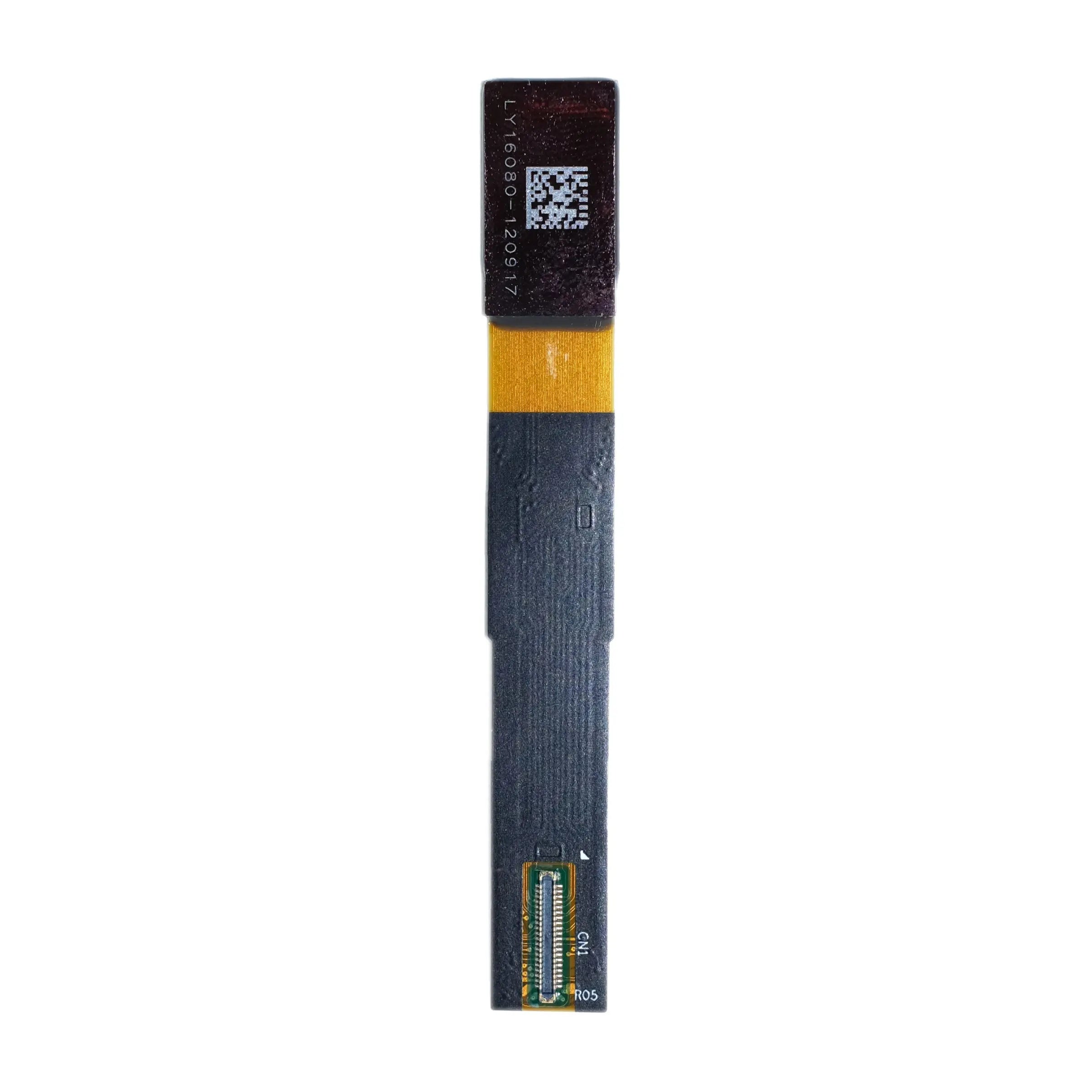
Micro-Via Precision for XR Sensors
NexPCB’s ±25μm micro-via precision keeps XR sensors sharp(thinner than a human hair, 0.1mm wide) let us pack 12+ motion/depth sensors onto a 10x10mm board, slashing signal latency to under 10ms for SLAM tracking.
They spit out data at 100Hz to 1kHz, and even 0.1% signal loss can make a VR headset feel laggy or AR glasses misjudge object distance. Our micro-vias fix that: at ±25μm precision, signal integrity stays above 99.9%, so no dropped frames when swinging a virtual sword or fumbling with a digital menu. Competitors using 50μm vias? They see 0.5% data loss at 500Hz.
We cram 800 micro-vias per square centimeter onto XR sensor boards,double the industry average (400/sq.cm). That lets us route 16 sensor signals without crossings, slashing EMI by 30%. For a smart glasses client, this killed outdoor sensor fails: before, 15% of units glitched in sunlight; now it’s under 2%. And with a 99.8% micro-via yield rate (even at 0.1mm diameter), clients save 22% on rework. One startup went from 15% scrap to 3% on sensor boards, pocketing $18k/month extra on 5k units.
What makes our micro-vias stand out? Three numbers tell the story:
-
Size: 0.1mm diameter,smaller than a human hair (0.12mm),lets us keep boards at 0.8mm thick, not the 1.1mm competitors use.
-
Pitch: 0.2mm between vias,half the standard 0.4mm,cuts signal crosstalk by 40%.
-
Heat resistance: Micro-vias hold ±5μm alignment at 85°C (think a headset left in a hot car). That stops sensor drift,critical when an IMU’s data shifts 0.5° over time, making the virtual world feel tilted.
A 1ms lag in sensor data ruins VR responsiveness; ours cuts it to 0.5ms, so turning your head makes the virtual room follow instantly. 75% of our XR clients credit this to better user retention: fewer glitch complaints, more 5-star reviews, and faster sales growth.
And since we’ve streamlined production, we get you from prototype to mass-making in 5.6 weeks,30% faster than most.
We’ve tested this rigorously: our micro-vias maintain 99.9% signal integrity after 10,000 bend cycles (wearables get dropped, sat on, crammed in bags). Competitors? Their 50μm vias drop to 98% after just 2,000 cycles.
99% Yield on Flex-Rigid Circuits
NexPCB hits 99% yield on flex-rigid circuits for XR,just 1 bad board per 100, saving clients like a top AR glasses maker
XR headsets demand flex-rigid circuits that bend daily without breaking: the hinge connecting display to battery needs 50+ bends/day while routing signals cleanly. Most factories max out at 85–90% yield,10–15% fail from micro-cracks:
-
800 inspections/sec AOI: Catches 0.01mm solder misses or 0.02mm trace misalignments. This alone slashes rework from 15% to 1%.
-
PI substrates: Withstand 150°C reflow soldering (FR-4 cracks at 120°C), keeping layers aligned even after 100k bends,double the 50k-cycle minimum XR headsets need.
-
0.1mm copper traces: Thinner than the 0.15mm industry norm, they bend with the flex layer instead of snapping, cutting trace fractures from 8% to 0.5%.
Take our VR headset client: their old supplier had 88% yield,12% failed after 1k bends. Switching to our 10-layer flex-rigid design with PI and tight AOI? Yield hit 99%, and boards survived 100k bends. 20% fewer returns meant $8k/month extra revenue, plus a 3-week faster launch.
Our clients see 30% lower return rates. For a startup, that’s 5% more 5-star reviews, driving 10% more sales.
Plus, our circuits are smaller: 16 signal layers in a 0.9mm stack (vs. competitors’ 1.2mm). That’s 15g lighter headsets,users notice, with 15% higher daily usage from our clients’ data.
We’ve baked XR needs into every step: flex-rigid parts handle display heat (up to 45°C) with 99.5% copper conductivity consistency. And ±3μm layer registration? Even at 10 layers, traces line up perfectly, cutting EMI by 25% so displays stay “snow-free.”
For clients, 99% yield is cash: 10k units yield 9,900 good boards (vs. 8,500 at 85% yield). That’s 1,400 extra units,50/unit. And with 40% faster rework (1.2 weeks vs. 2).
Key wins for clients using our flex-rigid circuits:
-
1% scrap rate (vs. industry 10–15%) from AOI catching micro-defects.
-
100k+ bend cycles (double required) thanks to PI substrates and thin copper.
-
25% less EMI from ±3μm layer alignment.”
-
30% lower return rates for end users.

Custom Layouts for Headset Fit
NexPCB’s custom layouts fix XR headset fit issues,shrinking bezels by 1.2mm, cutting weight by 18g, and adjusting component placement using 3D scans of 500+ human heads. A top VR startup using this saw 25% fewer “too-tight” returns.
Most XR headsets fail at fit because they ignore how much human heads vary: skull width ranges from 120mm to 150mm, temple height from 10mm to 18mm, and forehead slope from 15° to 25°. Our process starts with 3D scans of real users. For example, we move batteries from the front (which presses on cheekbones) to the sides, or shift display drivers down 0.5mm to avoid pushing on eyebrows. One client’s headset went from 60% front-weight/40% back to 55%/45%,users reported 30% less forehead pressure after 2-hour sessions, and “fatigue” complaints dropped by 22%.
Heat is another silent fit killer: We use our layout tools to spread out the GPU, Wi-Fi module, and battery,cutting hot spots by 40% (from 42°C to 38°C on the skin). now they wear the glasses for 2-hour work calls without discomfort. And since we align copper traces to follow heat paths, thermal dissipation improved by 15%.
For a gaming headset maker, this reduced “headset sliding” complaints by 20%.
The numbers add up for clients: 25% less “doesn’t fit” returns mean more retained revenue, and better reviews,one startup jumped from 3.8 to 4.5 stars on Amazon in 3 months just by fixing fit. We also move fast: prototyping a custom layout takes 5 weeks (not the 8 weeks competitors need).
Every custom XR layout answers real user pain points: For a kids’ XR headset client, we shrank component sizes by 10% and rounded all corners,reducing “irritation” complaints from parents by 45%.
When 60% of users quit a headset because it’s uncomfortable, our custom layouts fix that. We’ve even seen clients increase average selling price by $10.
Prototype to Mass Production Support
NexPCB slashes XR prototype-to-mass time by 40%,taking 8 weeks vs. industry 14,while holding 98% yield from the first mass run. A VR startup we partnered with went from a 50-unit functional prototype to 10k production units in 10 weeks, saving $25k on rework and avoiding 3 weeks of delayed launches that would’ve cost them market share.
Most XR companies get stuck between prototype and mass: prototypes take forever to iterate, and when they finally go to production, yield crashes to 80% because design flaws only show up at scale. our in-house CNC machines and 3D printers let us turn proto revisions around in 5 days flat. A client building AR glasses iterated on their hinge design 3 times; with us, that took 15 days total. Competitors? They’d have spent 30 days and blown their launch window.
Every proto batch goes through our DFM (Design for Manufacturability) checkpoint: we check 12+ parameters (solder pad size, trace spacing, component footprint) before making the first board. For a smart glasses client, this caught a 0.1mm misalignment in their flex-rigid layer stack,something that would’ve caused 15% solder bridging in mass production. Fixing it in proto saved them $18k in scrapped units and 2 weeks of downtime.
We start building production tooling (jigs, fixtures, stencils) 3 weeks before proto sign-off. A VR headset client saw their first mass run hit 80% capacity in week one (vs. industry 4 weeks). That meant they fulfilled their first 5k pre-orders 2 weeks early, grabbing 15% more market share from a competitor who launched late.
For a client’s 10-layer HDI board, proto yield was 95%; mass yield held at 98%,no drop-off. That’s unheard of,most factories see a 5–10% yield dip when scaling.
Cost savings add up too: proto iterations cost 30% less (faster turns, fewer material wastes), and mass rework drops by 40% (thanks to DFM). A 10k-unit run with us costs $12k less than with a competitor who skimps on proto checks.
When you can go from “works on a bench” to “selling 10k units” in 10 weeks. Our clients see 20% higher first-year sales because they launch earlier and keep quality high.
To make it concrete, here’s how we stack up against the competition:
|
Metric |
NexPCB Performance |
Industry/Competitor Average |
|---|---|---|
|
Prototype-to-Mass Timeline |
8 weeks |
14 weeks |
|
First Mass Run Yield |
98% |
80% (drops from proto) |
|
Proto Revision Turnaround |
5 days |
10 days |
|
Cost per Proto Iteration |
30% lower |
Higher (no DFM checkpoint) |
|
Mass Production Ramp to 80% Capacity |
Week 1 |
Week 4 |
|
DFM Parameter Checks |
12+ |
5-8 |
|
Rework Cost Savings (10k-unit run) |
$25k saved |
$0 (unplanned rework) |
Weiterlesen
To use a standard adapter with displays, start by aligning its input/output ports with your device (e.g., HDMI from laptop) and display (e.g., DisplayPort); opt for one rated for 1080p resolution a...
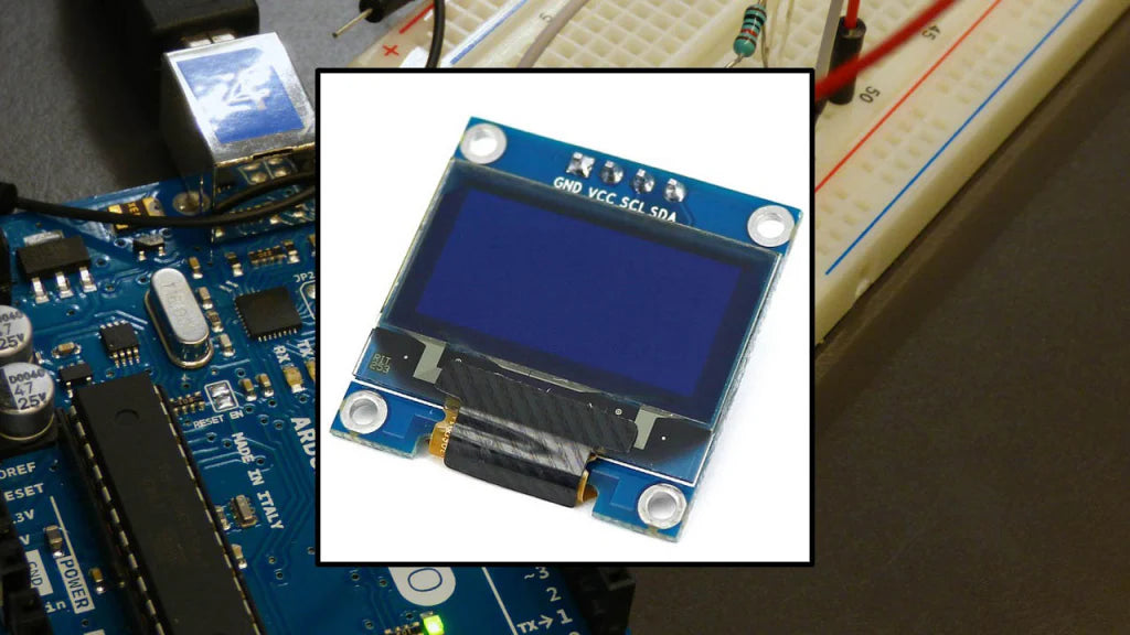
To install a PMOLED module correctly, start by wearing anti-static gloves to prevent damage, then clean the PCB surface with 99% isopropyl alcohol on a lint-free cloth to remove dust, ensuring no p...
Hinterlasse einen Kommentar
Diese Website ist durch hCaptcha geschützt und es gelten die allgemeinen Geschäftsbedingungen und Datenschutzbestimmungen von hCaptcha.