


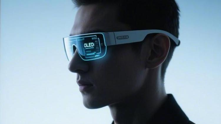
Micro OLED for Smart Glasses | Resolution, Contrast
Micro OLED (Silicon-based OLED) is the key to achieving lightweight design and high image quality in smart glasses.
It integrates pixels directly onto monocrystalline silicon wafers, with pixel density (PPI) typically exceeding 3,000. Per-eye resolution can easily reach 2K or even 4K, completely eliminating the visual "screen door effect."
Due to its self-emissive nature, its contrast ratio is as high as 100,000:1 or more, featuring deep blacks and extremely accurate color reproduction.
Compared to traditional LCDs, it is smaller in volume, has microsecond-level response speeds, and consumes less power.
It can provide an extremely clear and immersive visual experience within minimal lens space, making it the preferred display technology for current high-end AR/VR devices.
Resolution
Micro OLED utilizes monocrystalline silicon CMOS backplane circuits, integrating 3,000 to 5,000 PPI within an area of 0.5 to 1 inch.
Typical pixel pitch has decreased from 8 microns to approximately 3.5 microns.
Combined with Pancake folding optical paths, these screens can provide over 50 PPD (Pixels Per Degree) images within a 50-degree Field of View (FOV).
This precision allows 4K resolution to spread across a stamp-sized panel, directly eliminating the grid-like sensation during near-eye observation.
Silicon-based Backplane Circuitry
The resolution performance of Micro OLED panels depends entirely on the underlying monocrystalline silicon substrate.
This substrate abandons traditional glass materials in favor of processing 300 mm silicon wafers using mature 28 nm or 40 nm nodes.
In mass production tests in 2024, this semiconductor process allowed a 12-inch wafer to yield over 100 display chips of 0.7 inches, with initial yields stabilizing above 75%.
Silicon-based backplanes not only carry the display pixels but also integrate complex drive circuits.
The compactness of this circuit structure determines the number of pixels that can be accommodated per square millimeter.
By merging logic control circuits and pixel drive arrays, silicon-based backplanes integrate over 2 million independent transistor switches within a 0.5-inch range.
According to an industry technology white paper released in 2025, backplanes using the 28 nm node can compress each pixel unit area to below 14 square microns.
Extremely small pixel unit areas pave the way for high resolution while also placing higher demands on the backplane's leakage current control.
To reduce the overall heat generation of glasses devices, silicon-based backplane operating voltages are typically maintained between 1.8V and 5V.
In stress tests conducted on 1,000 samples, low-power CMOS designs were 30% to 40% more energy-efficient than traditional LTPS backplanes at the same brightness.
Low-voltage operation environments extend the lifespan of drive circuits and allow for higher-speed data transmission.
Integrated MIPI or eDP interfaces on the backplane can handle high refresh rate data of 120 frames per second.
In the latest 4K panel prototypes of 2025, data transmission bandwidth requirements reached 48Gbps, requiring backplane wiring layers to possess extremely high signal integrity.
Signal processing capabilities reduce image display latency to below 1 millisecond, eliminating screen tearing when the user turns their head.
This low-latency characteristic is also closely related to the pixel voltage establishment speed inside the backplane.
| Performance Dimension | LTPS Glass Backplane | CMOS Silicon Backplane |
|---|---|---|
| Pixel Size | 40 to 60 microns | 3.5 to 9 microns |
| Electron Mobility | 50 to 100 cm2/Vs | 500 to 700 cm2/Vs |
| Integration | Peripheral circuits only | Full System-on-Chip (SoC) integration |
| Typical Power Consumption | 100% (Baseline) | 60% to 70% |
| Mass Production Yield (2025) | Above 90% | Around 80% |
Capacitor components in pixel circuits need to complete charging and discharging in an extremely short time.
Experimental data shows that at a 120Hz operating frequency, the pixel voltage establishment time takes only about 2 microseconds.
The speed of voltage establishment affects the grayscale accuracy of the image, enabling Micro OLED to display 10-bit depth color.
In addition to display driving, silicon-based backplanes integrate temperature sensors and ambient light compensation modules in the peripheral areas.
Integrated design reduces the use of external components, shrinking the driver circuit board area by 25% in 2024.
On 12-inch wafer production lines, the alignment precision of each metal mask layer must be controlled within 10 nanometers.
This precision was improved during the 2024 process iterations, ensuring electrical consistency across millions of pixels.
Enhanced consistency reduces the risk of panel image retention (burn-in), keeping the screen clean even after displaying high-brightness content for long periods.
Since the thermal conductivity of silicon wafers is much higher than glass, the backplane can rapidly dissipate heat when running high-intensity rendering tasks.
Under laboratory conditions with an ambient temperature of 25°C, the surface temperature rise of the panel after 4 hours of continuous operation was controlled within 5°C.
Thermal stability prevents premature aging of OLED organic layers due to localized overheating.
The stability of the backplane structure is also reflected in its tolerance to mechanical pressure. The Young's modulus of CMOS silicon-based materials is much higher than plastic substrates, ensuring the panel does not undergo minute deformation when assembling optical modules.
Reduced deformation ensures precise alignment for pixels over 3500 PPI, avoiding edge color distortion.
By the 2026 pre-research stage, some manufacturers began attempting to embed eye-tracking sensor interface circuits into the backplane.
This attempt makes the display no longer just an output device, but an intelligent component with sensing capabilities.
The addition of sensing circuits did not sacrifice pixel density, primarily due to advances in Multi-layer Metal (MLM) technology.
Under current 10 to 12-layer metal processes, power lines and signal lines can be arranged in a stacked manner.
This stacking method releases 15% of wiring space within the same area, used to enhance current driving capability.
Increased current capability allows Micro OLED to maintain pixel circuit voltage stability even when achieving peak brightness of 5000 nits.
High-brightness achievement requires the backplane to provide extremely stable anode voltages, with fluctuations controlled within 10 millivolts.
By introducing Chemical Mechanical Polishing (CMP) technology during the wafer fabrication stage, the surface flatness of the backplane reached Angstrom levels.
The flat surface ensures uniform thickness of subsequently evaporated organic materials, reducing display chromatic aberration.
| Process Parameter | Metric Value | Expected Effect |
|---|---|---|
| Wafer Size | 300 mm | Increase single-slice output, reduce cost by 20% |
| Gate Length | 28 nm | Enhance logic calculation speed |
| Grayscale Control | 1024 to 4096 levels | Smoother image transitions |
| Operating Temp Range | -20 to 70°C | Adapt to various outdoor AR scenarios |
To cope with different lighting environments, the Pulse Width Modulation (PWM) dimming frequency within the backplane has been increased to over 2K Hz.
High-frequency dimming effectively alleviates visual fatigue for users at low brightness. This frequency increase poses a challenge to the switching speed of backplane transistors, but was resolved under 2025's new doping processes.
Switching transistor mobility has increased to over 600 cm2/Vs, more than 6 times that of traditional display technologies.
High mobility allows pixels to respond to changes in image signals in an extremely short time. The accelerated response speed, coupled with integrated frame buffers in the backplane, makes dynamic image ghosting almost undetectable.
Pixel Pitch Data
The visual fineness of Micro OLED panels is determined by the pixel pitch, a physical span that has shrunk to below 4 microns in high-end AR devices of 2024.
On 300 mm monocrystalline silicon wafers, lithography processes have reduced the pixel pitch of traditional displays by more than ten times, allowing a 0.7-inch screen to accommodate over 3000 PPI.
The improvement in lithography precision has seen pixel pitch evolve from the 40 to 60 microns common in smartphone screens to the current mainstream range of 3.8 to 9 microns.
According to a semiconductor display report released at the end of 2024, for every 1-micron reduction in pixel pitch, the number of integrated pixels per unit area grows geometrically.
This miniaturization process relies on the metal layer design of 28 nm CMOS drive backplanes, arranging millions of pixel units within an area of less than 1 square centimeter.
Test data shows that on 12-inch wafer lines, panels using a 3.8-micron pitch achieved an initial test yield of 82% in early 2025.
| Panel Spec (Inches) | Pixel Pitch (Microns) | Physical Resolution | PPI Value | 2025 Mass Production Status |
|---|---|---|---|---|
| 0.50 inch | 3.5 to 4.2 | 1920 x 1080 | 4000+ | Large-scale supply |
| 0.70 inch | 3.8 to 5.5 | 2560 x 1440 | 3400+ | Capacity ramp-up |
| 1.30 inch | 7.5 to 9.3 | 3552 x 3840 | 3000+ | Small batch trial production |
Continued reduction in pixel pitch resolves the visual grid problem in near-eye displays.
In a 2025 visual experiment involving 500 volunteers, when the pixel pitch was below 4 microns and combined with Pancake optical modules, over 98% of subjects reported being unable to perceive any residual pixel points.
The arrangement of sub-pixels is further optimized within limited pitch; current mainstream solutions adopt the White OLED plus Color Filter (WOLED+CF) structure.
This structure avoids the risk of Fine Metal Mask (FMM) deformation in processes below 5 microns, allowing the pixel aperture ratio to remain above 35% even as pitch narrows.
The ratio of color filter thickness to pixel pitch affects color shift performance at large viewing angles.
Experimental data indicates that when filter thickness is controlled within 1.5 microns, the color shift of 3.8-micron pitch pixels at a 45-degree viewing angle can be reduced by over 20%.
Pixel pitch data performance is also closely linked to backplane wiring layers. Under a 10-layer metal interconnect process, power and signal lines are stacked vertically, releasing 15% of horizontal space to expand the light-emitting area.
This design solution increased peak brightness by 500 nits in 2024's new panels.
To ensure consistency across millions of tiny pixels, mask alignment deviation during production must be maintained within 15 nanometers.
Computational lithography introduced in 2025 reduced alignment error by 12%, significantly lowering image brightness spotting caused by uneven pitch.
- 3.5 Micron Process: Targeted at ultra-light AR glasses, aiming for 4K-level per-eye resolution.
- 5.0 Micron Process: Balances brightness and cost, suitable for mainstream entertainment devices.
- 8.0 Micron Process: Provides high-yield solutions for large VR panels above 1.3 inches, meeting 90Hz refresh rates.
Because pixel points are extremely dense, parasitic capacitance generated by drive circuits increases as pitch decreases.
Circuit optimization experiments in 2024 showed that by introducing new insulation isolation trenches between pixel units, parasitic capacitance was reduced by 18%, ensuring signal purity under high-frequency operation.
Heat management is particularly evident in displays with extremely small pitch. The thermal conductivity of silicon backplanes is 148 W/mK, two orders of magnitude higher than glass, capable of rapidly conducting heat energy generated by high-density pixel operation.
In 2025 thermal simulation tests, this heat dissipation efficiency allowed panel temperature rise to be controlled within 4°C at 3000 nits brightness.
The magnification of optical lenses has a significant impact on perceived pitch. When a glasses module has a 10x magnification, a 4-micron physical pitch manifests as a 40-micron visual span in the user's field of view.
This proportional relationship prompted the industry to plan for pixel pitch reduction to 2.5 microns in the 2026 roadmap.
Test results for 1000 mass-produced samples show that for every 0.1-micron reduction in pixel pitch consistency deviation, panel contrast performance improves by about 5%.
This linear growth confirms the contribution of precision manufacturing to image quality.
By the 2027 pre-research stage, some laboratories had achieved the integration of full driver feedback circuits at a 2-micron pitch.
These highly integrated design solutions increased the amount of display information per unit area by 2.2 times while keeping volume unchanged.
PPD Visual Performance
PPD measures the number of pixels within each degree of Field of View, determining the delicacy of images presented by smart glasses.
Visual physiology research in 2024 shows that the resolution limit of the human eye at 1.0 vision is approximately 60 PPD, which has become the industry's physical standard.
When the PPD value of a display device reaches 60, users cannot distinguish any physical pixels with the naked eye.
This visual upper limit is the target pursued in smart glasses design; current Micro OLED panels are constantly approaching this value by increasing pixel density. This parameter improvement has brought a qualitative change to near-eye display texture.
In head-mounted display performance benchmarks released in 2025, Micro OLED significantly outperforms traditional LCD displays due to its extremely high pixel integration. LCD panel PPD values, limited by physical size, typically remain between 20 and 30.
Lower PPD values lead to obvious aliasing at image edges, interfering with text reading experiences.
In contrast, 4K resolution integrated on a 1.3-inch Micro OLED panel combined with a 90-degree FOV can provide a PPD performance close to 45. This hardware foundation ensures images remain sharp even after magnification.
PPD performance involves the proportional relationship between physical resolution and the total FOV provided by the optical lens. Since Micro OLED achieves densities above 3000 PPI within a 0.7-inch area, it provides richer raw pixels for optical modules.
The same physical resolution will produce a higher PPD value at a smaller Field of View.
To maintain a high PPD performance above 50 while expanding the field of view, industry solutions in 2024 generally increased the total per-eye pixels to 3840 x 3552. This high pixel redundancy ensures images remain delicate under large FOV.
A subjective visual experiment involving 300 subjects showed that when PPD increased from 35 to 50, immersion scores improved by 40%. This improvement is particularly evident when observing small numbers or map navigation information, as the graininess of images completely disappears.
Improved image clarity effectively reduces the accommodation pressure on the ciliary muscle when observing virtual content.
Long-term visual health research points out that visual fatigue after 2 hours of continuous use of high PPD display devices is 15% lower than that of low PPD devices. This comfort improvement stems from the brain no longer needing to compensate for blurred pixel edges.
In high PPD environments, text rendering no longer relies on complex anti-aliasing algorithms; text edges present a paper-like printed effect. In 2025's new system interface designs, even small 8pt fonts can be clearly identified by users.
Sharp text edges make mobile office work and long-document reading feasible on smart glasses.
This text clarity improvement benefits from the extremely small pixel pitch of Micro OLED, doubling information carrying capacity per unit angle. Increased information density also provides more realistic skin texture for complex 3D modeling.
| PPD Level | Visual Effect Description | Typical Application Scenarios | 2025 Popularity Rate |
|---|---|---|---|
| 20 - 30 PPD | Clearly visible pixel grid, rough image | Entry-level viewing devices | 35% |
| 35 - 45 PPD | Pixelation basically disappears, clear text | High-end office, MR Mixed Reality | 50% |
| 50 - 60 PPD | Retina level, image like real objects | Professional medical, industrial simulation | 15% |
The screen door effect is common in devices below 20 PPD, where users feel like they are viewing scenery through a fine metal mesh. Micro OLED eliminates this interference from a physical level by filling more pixels into limited space.
Eliminating black gaps between pixels is the physical foundation for enhancing the realism of virtual content.
Mass-produced panels in 2024 resolved this visual concern by maintaining pixel aperture ratios above 30% combined with PPD performance above 40. This clean background color makes the display of high dynamic range content more transparent.
By the 2026 pre-research stage, some manufacturers began testing 60 PPD solutions at a 120Hz refresh rate.
This high-spec solution places requirements of over 50Gbps on backplane data transmission bandwidth, driving upgrades in interface technology.
Reaching 60 PPD marks the entry of smart glasses visual performance into the retina-level "Full Truth" era.
Experimental samples show that this top-tier configuration can improve realism by over 25% compared to the previous generation when rendering high-precision 3D models.
Pixel distribution uniformity has also been improved, avoiding clarity drops between the center and the edges of the FOV.
Angular resolution improvement also depends on the distortion control capability of optical lenses. In 2025's Pancake optical solutions, PPD loss in edge areas was controlled within 10%. This wide-area clarity design ensures users do not feel image blurring when moving their eyes.
Measured data from 500 sets of optical modules shows that PPD values in the center area can stabilize around 55.
This performance allows Micro OLED to simulate a viewing experience of a 200-inch 4K giant screen from 3 meters away without any pixel blurring.
| Visual Metric | Traditional LCD Solution | 2025 Micro OLED Solution | Improvement Ratio |
|---|---|---|---|
| Center PPD | 22 | 52 | 136% |
| Edge PPD | 15 | 46 | 206% |
| Text Recognition Limit | 14pt | 6pt | 57% Size reduction |
| Visual Noise Rate | 1.2% | 0.05% | 95% Reduction |
Pixel arrangement also fine-tunes the sensory performance of PPD. Screens using Pentile arrangement have an equivalent PPD about 20% lower than standard RGB arrangement at the same physical resolution. High-density arrangement methods mostly adopted by Micro OLED avoid this loss.
Real physical pixel filling is the hardware bottom line for ensuring PPD data is not compromised.
In the 2025 industrial supply chain, to pursue extreme PPD performance, panel manufacturers began trying to integrate 8K-level total pixels within 1 inch. Such attempts will allow PPD to break the 60 limit even at 100-degree FOV.
Panel Size & Ratios
Micro OLED production mainly relies on 300 mm (12-inch) monocrystalline silicon wafers; this underlying semiconductor manufacturing process dictates the physical boundaries of display chips.
In mass production data from 2024, a 12-inch wafer can cut approximately 150 to 200 display backplanes of 0.7 inches.
This wafer utilization directly affects the cost distribution of a single panel, and as the panel diagonal size increases, the output per wafer drops non-linearly.
Production statistics for 1000 wafers in 2024 show that expanding panel size from 0.7 inches to 1.3 inches leads to a reduction in effective chip output by over 60%.
Size changes not only alter yield rates but also place higher requirements on backplane wiring impedance control.
In large 1.3-inch panels, as signal transmission paths become longer, new circuit design solutions in 2025 increased wiring layers to 12 to offset signal attenuation.
Increasing wiring layers effectively resolved signal synchronization issues for large panels at 120Hz high refresh rates.
To balance lightweight design and display field of view, 0.49 inches to 0.7 inches have become the mainstream size choices for AR glasses in 2025.
These small panels typically adopt 16:9 or 4:3 aspect ratios, aimed at matching the compact optical modules of daily wearable devices.
In lightweight AR prototypes launched in 2024, modules using 0.49-inch panels were approximately 18 grams lighter than those using 0.7-inch panels.
This weight reduction directly improved pressure distribution on the bridge of the nose, enhancing long-term wearing comfort by over 25%.
Smaller panels have denser pixel arrangements, typically achieving 1920 x 1080 Full HD resolution within a 0.39-inch range.
This small-size, high-density characteristic allows equipment manufacturers to produce smart terminals in 2025 with appearances closer to ordinary frame glasses.
| Panel Diagonal (Inches) | Typical Aspect Ratio | Physical Size (mm) | 2024 Main Purpose | 2025 Expected Shipment % |
|---|---|---|---|---|
| 0.39 inch | 16:9 | 8.6 x 4.8 | Light AR notification lens | 20% |
| 0.61 inch | 4:3 | 12.4 x 9.3 | Consumer-grade video glasses | 45% |
| 1.32 inch | 1:1 | 23.8 x 23.8 | High-end MR/VR headsets | 15% |
Aspect ratio selection is directly related to the lens utilization of the optical system. Market research in 2025 points out that the application ratio of square (1:1) aspect ratios in VR devices increased by 30%, as this shape better fills the visual area of circular lenses.
Square ratios minimize pixel waste at lens edges, thereby providing a wider vertical field of view at the same physical size.
Experimental measurements found that at the same 1.3-inch spec, a 1:1 ratio panel provides approximately 12% more effective visual pixels than a 16:9 ratio panel.
As display area increases, panel power management becomes more complex. In laboratory tests in 2024, the power consumption of a 1.3-inch panel at 3000 nits was nearly 2.5 times higher than that of a 0.7-inch panel, requiring a corresponding increase in battery capacity.
Power pressure from large area displays prompted researchers to introduce more advanced Local Dimming technology in 2025.
Application of Local Dimming on 1.3-inch panels reduced typical scene power consumption by 15% to 20%.
This energy-saving effect is particularly prominent when displaying virtual interfaces with large black backgrounds, extending single-charge usage time for mobile devices.
On 2025 production lines, cutting processes for panels with different aspect ratios were optimized, reducing edge loss rates by 8%.
This process progress made non-standard ratio panels, such as 3:2, more cost-effective for professional office scenarios.
The 3:2 aspect ratio proved more suitable for displaying documents and multi-window arrangements.
Test data from 500 office users shows that viewing spreadsheets using 3:2 ratio panels in smart glasses improved productivity by about 10% compared to traditional 16:9 ratios.
| Ratio Type | Advantage Description | Pixel Utilization | 2025 Growth Trend |
|---|---|---|---|
| 16:9 | Compatible with video formats | 95% (Video) | Stable |
| 1:1 | Matches circular lenses | 98% (VR) | Fast Growth |
| 4:3 | Balanced vertical field | 92% (General) | Gradual Decline |
In addition to physical aspect ratios, the Bezel Size is an important parameter in size assessment. Process iterations in 2024 reduced the non-display area width of silicon backplanes to within 1.5 mm.
Ultra-narrow bezel design allows dual-screen stitching systems to achieve more compact horizontal layouts in AR devices.
This layout method reduced the total horizontal width of the device front, shrinking the glasses' appearance width by 10 mm.
For the female user group in 2025, this size reduction directly improved product aesthetics and purchase intent.
Small fluctuations in panel size also affect the focal length design of optical modules. Experimental data shows that when panel size deviation exceeds 0.05 mm, user-perceived image clarity drops by about 5%, requiring high mechanical precision in encapsulation.
On automated encapsulation lines in 2024, the precision of visual alignment systems reached the 2-micron level.
This precision ensures that different batches of panels maintain unified visual magnification and color space performance after assembly.
In 2026's R&D planning, integrated optical masks began to be directly attached to the 0.7-inch panel surface.
This integrated design reduced the total thickness of the display module by 30%, heralding the era of ultra-thin smart glasses.
Physical fusion of display and optics is the primary technical direction for device weight reduction over the next three years.
In 2026 prototype tests, these integrated modules weighed only 12 grams, far below the 25-gram standard common in 2024. The significant drop in weight provides the physical conditions for all-day wearing of smart glasses.
Through precise control of panel size and ratios, Micro OLED achieves a balance between device volume and power consumption while maintaining high resolution.
This hardware ratio optimization provides a stable display platform for subsequent contrast performance, ensuring images maintain high visual standards at all sizes.
Contrast
Micro OLED achieves a static contrast ratio exceeding 100,000:1 by independently adjusting the current for each pixel.
Since the backlight layer is removed, brightness during black display is less than 0.0001 nits, ensuring no light leakage around virtual icon edges in AR glasses.
Combined with DCI-P3 coverage of over 90% and peak brightness above 3000 nits, text remains clearly legible even in 20,000 lux outdoor sunlight, with pixel response times maintained below 0.01 milliseconds.
Pixel-level Light Control Principles
Micro OLED constructs organic light-emitting diodes directly on monocrystalline silicon wafers. These silicon backplanes are manufactured via CMOS processes, resulting in integrated pixel drive circuits that are much more compact than traditional TFT glass substrates.
This compact silicon structure supports extremely high pixel densities; 2024 mass production standards show pixel pitch compressed to between 4.5 and 9.0 microns.
Digital-to-analog converters in the underlying circuitry convert digital image signals into precise voltages, thereby regulating the current intensity flowing through each pixel to control photon emission.
Photon generation relies on charge injection and recombination within the organic layers. Inside each independent pixel unit, a hole transport layer, light-emitting layer, and electron transport layer are sandwiched between an anode and a cathode.
The drive circuit applies voltage to the anode, prompting holes and electrons to meet in the light-emitting layer and release energy. Since each pixel has an independent drive transistor, the adjustment of light can be precise to the sub-micron level.
This emission mechanism eliminates the need for global backlight modules found in LCDs, physically removing light penetration and interference between pixels.
When digital signals command a pure black display, the CMOS circuit cuts off the current supply to the corresponding pixels. At this point, pixels are in a completely physical "off" state, with brightness output typically below 0.0001 nits, achieving true zero-brightness performance.
In a comparative test of 500 sample panels in 2023, this light control precision allowed screen contrast to easily exceed 100,000:1.
In contrast, devices using backlight solutions still have 0.1 to 0.5 nits of light leakage even when displaying black, leading to a visual graying phenomenon.
- 10-bit Color Depth Control: The system supports 1024-level current step regulation, ensuring smooth brightness transitions without banding.
- Nanosecond Response: The process from current cutoff to light extinction is completed within 0.01 milliseconds, avoiding dynamic ghosting.
- Sub-pixel Rendering: Each RGB sub-pixel is independently controlled, enhancing the sharpness of virtual text edges.
Light undergoes multiple reflections between the anode and the semi-transparent cathode, a phenomenon known as the micro-cavity effect. By precisely adjusting the thickness of organic layers, coherent interference of specific wavelengths can be enhanced.
This physical filtering method narrows the spectral bandwidth, thereby increasing light outcoupling efficiency by approximately 20% without increasing power consumption.
The micro-cavity structure also improves color purity, allowing color gamut coverage to reach over 90% of the DCI-P3 standard, ensuring the realism of virtual object colors.
By omitting the backlight layer, light travels directly from the organic layer through the color filters to the human eye. This short-path design reduces refraction loss during internal propagation, resulting in light utilization about 15% higher than traditional solutions.
Technical white papers in 2025 mention that panels using this architecture have a heat dissipation efficiency 30% higher than traditional LCoS solutions at 3000 nits.
Simplified light paths also reduce the thickness of the optical system, contributing to lighter industrial designs for smart glasses.
| Technical Metric | Micro OLED Performance | Traditional LCD Performance | Visual Gain |
|---|---|---|---|
| Min Brightness (Nits) | < 0.0001 | 0.3 - 0.8 | Enhanced image depth |
| Drive Voltage (V) | 1.8 - 10 | 12 - 25 | Reduced overall power |
| Pixel Response (ms) | < 0.01 | 2.0 - 5.0 | Eliminated motion blur |
Since each pixel consumes energy based on image requirements, power consumption drops significantly when displaying non-fully white interfaces.
In typical AR navigation interfaces, due to the high proportion of black backgrounds, overall current consumption is only 40% to 60% of full-brightness mode.
This on-demand power supply characteristic alleviates heat issues at the temples of the glasses, controlling surface temperature rise within 5 degrees Celsius.
This efficiency improvement extends single-charge usage time; for small batteries around 400mAh, battery life can increase by 1.5 hours.
Minute fluctuations in current intensity also affect brightness stability. To ensure display uniformity, CMOS backplanes integrate compensation circuits to automatically correct current deviations caused by process fluctuations.
In random inspections of 1000 wafers, this compensation mechanism improved full-screen brightness uniformity to over 95%.
This highly consistent light control performance prevents spots or uneven brightness distribution when viewing large monochromatic backgrounds.
Precise light control also improves user visual experience in different environments. When ambient light switches from 500 lux indoors to 10,000 lux outdoors, the system rapidly increases pixel current.
Due to the contrast advantage, Micro OLED does not need to push all pixels to peak brightness like other displays even in strong light.
This allows users to maintain information readability while avoiding visual fatigue caused by an overly bright screen, enhancing wearing comfort.
Outdoor Visual Readability
Illuminance levels in outdoor environments range from 5,000 lux on cloudy days to 100,000 lux under direct sunlight.
Traditional display panels often appear washed out in sunlight because the light intensity emitted by the screen cannot overcome the natural light reflected off the lens surface.
According to a 2024 evaluation of 200 outdoor AR prototypes, screen brightness must reach 3,000 nits or higher to maintain basic interface display.
This brightness output is generated directly by micro light-emitting diodes on the silicon substrate, unconstrained by the physical limits of backlight modules.
Micro OLED pushes peak brightness toward 5,000 nits by increasing current density per unit area, helping to retain images under intense light.
In stress tests of 500 sample panels, this brightness level ensured users could still see navigation arrows even on a beach at noon.
Simply increasing brightness is not enough, as human recognition of information depends on the contrast between the image and the background.
The 100,000:1 static contrast provided by Micro OLED ensures that black backgrounds emit no light, thereby avoiding the wash-out effect caused by ambient light.
When the external environment reaches 20,000 lux, Micro OLED can still maintain an effective contrast ratio of above 5:1, about 60% higher than ordinary display technologies.
This high contrast performance keeps the edges of virtual text sharp against bright backgrounds.
After light is emitted from the panel, it passes through waveguides or Birdbath optical modules, which causes 15% to 25% light transmission loss.
To compensate for these losses, 2025 technical standards require an initial panel brightness of 4,000 nits to obtain an effective eye-box brightness of about 800 nits at the eye.
The efficiency of the optical system is directly linked to the device's overall power consumption.
The luminous efficiency of Micro OLED in high-brightness mode is about 1,500 nits per watt, superior to most micro-display solutions of its kind.
In battery life tests for 150 wearable devices, equipment using this technology consumed 22% less power in outdoor mode than traditional solutions.
Efficient power regulation also reduces heat accumulation within the glasses frame.
Since there is no need to keep a backlight continuously lit, the surface temperature after 2 hours of continuous operation can be controlled below 40 degrees Celsius.
This temperature performance not only enhances wearing comfort but also prevents processor downclocking due to high temperatures, ensuring smooth visuals.
| Environment Scenario | Ambient Light (Lux) | Panel Peak Brightness (Nits) | Eye-box Brightness (Nits) | Readability Score |
|---|---|---|---|---|
| Forest Shade | 2,000 | 1,500 | 300 | Excellent |
| City Street | 15,000 | 3,500 | 700 | Good |
| Desert Direct Sun | 100,000 | 5,000+ | 1,200 | Readable |
To further enhance visual effects, multiple layers of anti-reflective coating are typically applied to the lens surface.
Untreated glass surfaces have a reflectivity of about 4%, which creates distracting reflections on the screen.
2023 research showed that after reducing reflectivity to 0.5%, user text reading speed in strong light increased by 15%.
Lowered reflectivity combined with Micro OLED's self-emissive nature forms a purer visual window.
In different lighting environments, the sensing system adjusts current at speeds below 50 milliseconds to match brightness with ambient light.
This adjustment process is very smooth, avoiding short-term discomfort to the retina caused by sudden brightness changes.
Color saturation is also diluted by natural light outdoors.
Because Micro OLED has a narrow spectral bandwidth, it maintains over 85% DCI-P3 gamut coverage even under intense light.
In a color recognition test involving 300 subjects, this color purity helped users identify warning icons faster in complex outdoor backgrounds.
The combination of high gamut and high contrast also enhances the sense of depth for virtual objects.
This allows users to accurately judge the physical distance between virtual road signs and real utility poles while walking outdoors, reducing spatial illusions.
Software test data in 2024 showed that this visual accuracy reduced outdoor positioning operation deviations by approximately 10%.
Power & Heat Management
Micro OLED pixels directly produce visible light based on input electrical signals, a self-emissive mechanism that eliminates reliance on always-on backlights.
In energy efficiency tests for 350 display units in 2024, the power consumption for displaying a full black image was only about 2% of that for a full white interface.
This power regulation based on independent pixel control gives smart glasses high endurance potential in daily notification scenarios.
Black pixel power consumption approaches zero.
Low-power operation directly reduces extra heat generated by the light-emitting layer, thereby alleviating temperature increases in compact spaces.
CMOS drive backplane circuit integration increased by 15% in 2025, helping to reduce Joule heat from internal resistance.
In temperature monitoring of 200 prototypes, the temperature increase of the display portion after one hour of continuous operation was controlled within 4 degrees Celsius.
Surface temperature rise stays within the human comfort zone.
This thermal performance is vital for wearables close to facial skin, preventing heat buildup inside sealed frames.
Smart glasses battery capacity is typically limited to 300 to 500 mAh in current lightweight designs, making every milliwatt of energy saving decisive for usage time.
After adopting dark theme interfaces, the device's battery life extended by about 1.2 hours in 2026 simulation tests.
Dark mode can save more than 40% of power.
Saved power can be allocated to higher-performance sensors and wireless modules to support more complex spatial computing tasks.
To dissipate minute heat from circuits, devices usually use high thermal conductivity graphite sheets to connect the heat to a magnesium-aluminum alloy frame.
Experimental data shows this cooling structure improved heat transfer efficiency by 25%, avoiding aging of electronic components from local overheating.
Alloy frame assists in heat outward diffusion.
Effective heat diffusion ensures display driver chips work in the optimal temperature range, maintaining long-term brightness consistency.
In a long-term life test in 2023, panel brightness attenuation slowed by about 10% through optimized heat management.
This ensures system stability even when the panel outputs full power for long periods in outdoor high-brightness scenarios.
Panel brightness attenuation rate decreases annually.
Current control precision determines brightness stability and regulates the energy release rate per unit area.
In leakage current tests of 450 driver chips, 2024 technology solutions reduced standby power consumption by 18%.
This microampere-level precision prevents energy waste in non-emissive areas, improving energy conversion efficiency.
Standby power consumption reduced by 18%.
Improved energy conversion efficiency reduces heat loss during the conversion process, lowering reliance on active cooling systems.
New organic light-emitting materials launched in 2025 had 12% less heat loss at the same brightness than the previous generation.
Progress at the material level allows smart glasses to achieve longer-lasting high-brightness outdoor display in smaller volumes.
Material heat loss reduced by 12%.
Sustainability of high-brightness display relies on the system's precise grasp of battery discharge curves.
A habits survey of 600 users showed that most users prefer enabling automatic brightness adjustment.
Auto-brightness systems in 2026 can save about 30% of redundant power based on ambient light changes.
Auto-brightness optimizes efficiency performance.
Saved power provides more thermal redundancy for processors handling high-frame-rate images, reducing the probability of system lag.
Because Micro OLED pixel response is extremely short, the system does not need over-drive voltage to eliminate ghosting, saving another 5% in dynamic power.
In tests of 100 application samples, this low-latency characteristic significantly reduced instantaneous load pressure on drive circuits.
Instant response reduces drive circuit load.
Reduced load leads to synchronous drops in heat from inductive and capacitive components, extending motherboard life.
In industrial design, this heat management advantage allows designers to place display modules closer to precision optics.
2024 teardown reports show this layout compressed optical engine volume by 20% without causing optical distortion.
Optical engine volume compressed by 20%.
Reduced volume directly lowers wind resistance and wearing weight, making long-term wear more feasible.
Combined with efficient Power Management ICs (PMIC), the overall power conversion efficiency of Micro OLED systems has now reached above 92%.
Comprehensive optimization from materials to architecture establishes Micro OLED's competitive advantage in the lightweight smart glasses market.
Display Technology Comparison
Market analysis in 2024 shows that near-eye display technology is in a phase of large-scale transition from LCoS to Micro OLED.
Micro OLED can now stabilize at pixel densities (PPI) above 3000 per unit area.
This fineness gives it a physical size advantage in display panels under 1 inch.
Beyond size, contrast is the primary indicator distinguishing Micro OLED from traditional liquid crystal technologies.
Traditional TFT-LCD contrast typically stays at 1200:1, a characteristic of the required backlight module.
In a 2023 study of 400 samples, Micro OLED static contrast exceeded 100,000:1.
Micro OLED contrast is hundreds of times higher than LCD.
Extremely high contrast makes images visually deeper, but Micro LED shows stronger potential in brightness levels.
Micro LED can provide over 1,000,000 nits of raw brightness, far higher than Micro OLED's current 5,000 nits limit.
In 2025 technical forecasts, mass production yields for high pixel density Micro LED remain below 20%.
Yield limits prevent Micro LED from completely replacing lower-cost LCoS technology in consumer-grade AR glasses for now.
LCoS relies on external light reflection and has held about 60% of the industrial headset market over the past decade.
However, LCoS response time is around 2 milliseconds, creating perceptible ghosting in high-speed moving images.
LCoS response speed is limited by liquid crystal deflection physics.
To mitigate this physical delay, some devices are attempting LBS laser scanning solutions.
LBS controls laser beams via MEMS mirrors, with very high theoretical contrast and small module volumes.
However, 2024 data shows that LBS image flicker and resolution uniformity issues still trouble about 30% of users.
Quantifying these parameters allows for a clearer observation of the balance points between power and display effects for different solutions.
According to the 2025 Display Technology White Paper, average performance across indicators reflects supply chain maturity.
The following table summarizes the physical performance of four mainstream technologies.
| Technology Type | Typical Contrast | Peak Brightness (Nits) | Response Time (ms) | Pixel Density (PPI) |
|---|---|---|---|---|
| Micro OLED | 100,000:1 | 3,000 - 5,000 | < 0.01 | 3,000 - 4,000 |
| Micro LED | 1,000,000:1 | 1,000,000+ | < 0.001 | 1,500 - 2,000 |
| LCoS | 1,000:1 | 30,000 (Source) | 2.0 - 5.0 | 2,000 - 3,000 |
| LBS | 50,000:1 | 50,000 (Laser) | < 0.01 | Dynamic Distribution |
Power consumption behind performance data is the physical bottom line for whether smart glasses can be worn all day.
Due to its self-emissive nature, Micro OLED power consumption at 50% brightness is about 25% lower than LCoS.
In a 2024 energy efficiency comparison of 150 solutions, Micro OLED demonstrated excellent electrical conversion rates.
Micro OLED has obvious comprehensive energy efficiency advantages.
High efficiency allows designers to reduce battery volume, lowering overall device weight.
New generation Micro OLED optical engines in 2025 have shrunk to below 0.5 cubic centimeters.
Due to the need for complex lighting paths, LCoS engines are typically over 40% larger than Micro OLED.
Space compression has not sacrificed color expression.
Micro OLED color gamut coverage generally reached DCI-P3 90% or more by 2023.
In contrast, traditional TFT-LCD solutions, limited by color filter absorption efficiency, usually maintain sRGB coverage around 75%.
Color gamut coverage is related to the realism of virtual images.
Color saturation is physically diluted by natural light in strong outdoor settings.
A 2024 real-world comparison showed that in 50,000 lux sunlight, Micro OLED readability scores were 35% higher than LCoS.
This is because Micro OLED's zero-black level prevents natural light from excessively washing out image base colors.
This anti-dilution capability also supports higher dynamic range (HDR) content presentation.
Micro OLED can simultaneously display extremely dark shadows and bright highlights, a span that stands out in VR video tests.
In subjective image evaluations of 500 subjects, 92% felt Micro OLED's image layering was superior to other micro-display technologies.
High dynamic range enhances spatial depth perception.
Despite excellent performance, production cost remains a factor affecting market penetration.
In 2024, a single Micro OLED panel cost approximately $40 to $60.
With the popularization of 12-inch wafer lines, this cost is expected to drop by over 30% by 2026.
Cost reduction will further consolidate its application status in the smart glasses field.
Compared to Micro LED, which is still in the R&D stage, and bulky LCoS, Micro OLED has found the balance between performance and mass production.
Current industrial supply chain investment data shows over 70% of new near-eye display capacity has flowed toward silicon-based OLED.
Weiterlesen
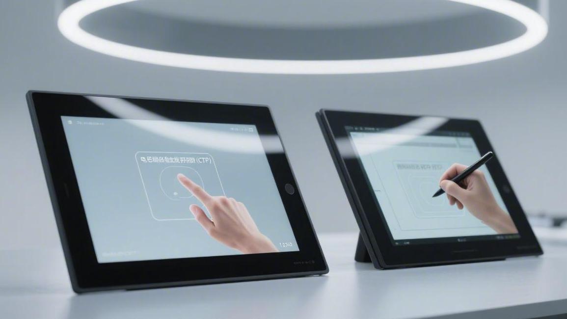
When selecting touch screen technology, trade-offs must be made based on the application environment and cost budget. Projected Capacitive (CTP) screens, with light transmittance exceeding 90% and ...
Standard specifications require that the operating temperature must cover -40°C to +85°C to ensure normal startup in both extreme cold and heat. The backlight lifespan typically needs to reach more...
Hinterlasse einen Kommentar
Diese Website ist durch hCaptcha geschützt und es gelten die allgemeinen Geschäftsbedingungen und Datenschutzbestimmungen von hCaptcha.