


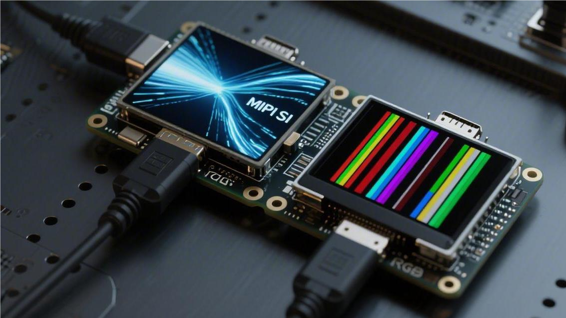
MIPI DSI vs RGB Interface | Bandwidth, Resolution & Integratio
The MIPI DSI single-lane bandwidth reaches up to 4.5 Gbps, requiring only 4 sets of differential lines to support 4K high resolution. It features strong anti-interference capabilities and is extremely easy to integrate into compact devices.
In contrast, the RGB parallel interface requires over 20 data lines, leading to complicated routing and a large footprint. Its limited bandwidth typically restricts its resolution to 1080P.
Bandwidth
The RGB display interface uses a structure with 24 data lines and an independent clock line. Limited by signal crosstalk between the lines, its maximum clock frequency is capped at around 150 MHz, and the overall data throughput stagnates at approximately 3.6 Gbps, supporting a maximum image output of 1920×1080@60Hz.
MIPI DSI utilizes low-voltage differential signaling for serial transmission. Taking the D-PHY standard as an example, the speed of a single data lane ranges from 1.5 Gbps to 2.5 Gbps.
Under a 4-lane configuration, the total bandwidth reaches 10 Gbps, providing the hardware foundation to output 4K resolution and 120Hz images.
The physical differences in signal transmission modes dictate a nearly 3-fold throughput gap between the two.
Signal Transmission
Under a 24-bit color depth configuration, the main control chip needs to simultaneously output 24 data lines, plus an independent clock signal line (PCLK), a vertical sync line (VSYNC), a horizontal sync line (HSYNC), and a data enable line (DE). The multi-channel physical structure requires the voltage levels on the lines to make full-swing transitions between 0V and 1.8V or 3.3V.
High-amplitude level transitions consume a significant amount of charging and discharging time, suppressing the headroom for clock frequency improvements. When the PCLK frequency is increased beyond 100 MHz, the PCB trace length matching errors among the 28 signal lines can easily cause Signal Skew. To ensure timing synchronization, engineering specifications mandate that the routing length error between the RGB data lines and the clock line must be controlled within 10 mils (about 0.254 mm), which drastically increases the difficulty of PCB routing.
-
Adopts single-ended signal transmission/reception, resulting in weaker resistance to external electromagnetic interference.
-
Large level transition amplitudes (1.8V/3.3V) lead to relatively high overall power consumption.
-
Highly susceptible to generating high-intensity electromagnetic interference (EMI) under high-frequency operating conditions.
-
Routing must adhere to extremely tight length matching tolerances (within 10 mils).
-
A massive pin count of 28 occupies a significant amount of physical PCB space.
Physical transmission bottlenecks drove the shift of display interfaces towards serial differential signaling. The MIPI DSI D-PHY physical layer completely abolished independent synchronization signal lines, packing all video data and control commands into fixed-format Packets. The master end relies solely on one pair of Clock Lanes and 1 to 4 pairs of Data Lanes to send low-voltage differential signals to the screen. Two wires transmit electrical levels of opposite polarities, and the receiving end determines logical 0 or 1 by measuring the voltage difference.
The common-mode voltage for differential transmission is set around 1.2V, while the differential-mode voltage swing is only 200mV (i.e., between +100mV and -100mV). This tiny level transition amplitude significantly shortens the rise and fall times of the signal, easily allowing a single lane's transmission rate to exceed 1.5 Gbps. The physical characteristic of opposing electromagnetic fields canceling each other out reduces radiation interference in the hundreds of megahertz to gigahertz frequency bands to extremely low levels.
To balance high-speed video output with low static power consumption, the D-PHY physical layer is designed with two distinctly different operating states. When transmitting high-resolution video streams, the interface enters High-Speed (HS) mode, running at full speed using 200mV low-voltage differential signals. When the screen displays a static image or only needs to send low-speed control commands, the interface quickly switches to Low-Power (LP) mode, reverting to single-ended levels with a swing increased to 1.2V and the rate dropped to 10 Mbps.
-
Packet-based serial communication protocol architecture.
-
Differential pair routing design with built-in high common-mode noise suppression capability.
-
Follows strict 100-ohm (±10%) differential impedance control specifications.
-
Supports dual-mode switching between HS (High-Speed) and LP (Low-Power).
-
Minimalist pin design, requiring a minimum of only 4 wires (1 clock pair + 1 data pair).
As panel refresh rates climbed, the MIPI Alliance introduced the upgraded C-PHY standard. C-PHY abandons the traditional two-wire differential pair and instead uses three wires to form a data group (Trio). At any operating moment, the three wires independently maintain three different voltage states: high, medium, and low levels. The receiving end decodes the specific data content by comparing the voltage differences between any two of the wires.
The 3-Phase Symbol Encoding mechanism allows C-PHY to map 2.28 bits of data to the waveform changes of a single clock cycle. Compared to D-PHY, under the same signal toggle rate, C-PHY's data throughput efficiency is significantly boosted. When the operating clock is set to 2.5 Gsymbol/s, the actual data throughput of a single Trio can reach 5.7 Gbps, greatly alleviating the routing pressure for high-resolution screens.
High-speed differential signals impose stringent impedance and spacing metrics on hardware PCB routing. Each pair of MIPI lanes must comply with a 100-ohm (±10%) differential impedance requirement. When laying out PCB traces, the intra-pair length matching error of the two wires within a lane must be controlled to within 5 mils (about 0.127 mm), while the inter-pair length error between different lanes is relaxed to within 150 mils. This relaxation benefits from the Lane Deskew mechanism embedded in the serial protocol.
The buffer memory (FIFO) of the receiving chip temporarily stores the data packet sequences that arrive earlier from various lanes. The protocol specification defines a special Sync Word, usually containing the fixed identifier 0xB8. After the chip detects the sync word from each lane, it aligns the data packets at the internal logic level, eliminating nanosecond-level delay errors caused by unequal physical routing lengths, thus restoring completely flawless video frames.
Hardware Parameter Comparison
When the main controller outputs an RGB video stream to the display panel, a conventional 24-bit color depth PCB needs to reserve at least 28 physical pins. 24 traces are responsible for transmitting 8-bit binary pixel data for R, G, and B colors, while the remaining 4 are allocated to PCLK, HSYNC, VSYNC, and DE sync signals. FPC (Flexible Printed Circuit) connectors usually need to reach 40 to 50 contacts to accommodate additional power lines, ground lines (GND), and backlight control pins.
The massive number of physical contacts creates a physical obstacle to narrowing the bezels of terminal devices, and the width of a 40-pin FPC connector generally exceeds 20 mm. The MIPI D-PHY specification replaces parallel pixel buses with high-speed serial lanes. In a standard 4-lane configuration, only 4 pairs of Data Lanes and 1 pair of Clock Lanes need to be reserved, reducing the total number of signal pins to 10.
This pin reduction saves physical PCB layout area. The 10 contacts can be physically docked using a miniature B2B (Board-to-Board) connector with a 0.4 mm pitch, reducing the overall length of the connector to less than 5 mm.
| Interface Type | Number of Pixel Data Lines | Number of Clock/Sync Lines | Total Signal Pins | Typical FPC Connector Width |
|---|---|---|---|---|
| 24-bit RGB | 24 | 4 (PCLK/H/V/DE) | 28 | > 20 mm |
| MIPI D-PHY (4-Lane) | 8 (4 pairs of diff lines) | 2 (1 pair of diff lines) | 10 | < 5 mm |
| MIPI C-PHY (3-Trio) | 9 (3 sets of 3-phase lines) | 0 (Clock Embedded) | 9 | < 5 mm |
The voltage swings measured by an oscilloscope exhibit different waveform heights. When parallel RGB ports output TTL levels, the peak voltage is typically set at 3.3V or 1.8V. For every pixel refreshed on the screen, some of the 24 data lines must complete a massive capacitive charge and discharge cycle between 0V and 3.3V, causing the overall line power consumption to reach hundreds of milliwatts.
The introduction of low-voltage differential signaling changed the current flow of the power supply architecture. When MIPI D-PHY is in High-Speed (HS) transmission mode, the two wires maintain a common-mode voltage (Vcm) of about 1.2V. The high-low logic toggle amplitude measured by a differential probe is strictly compressed within a 200mV (±100mV) range. This minute voltage jump lowers the dynamic power consumption of both the transmitter and receiver down to the scale of tens of milliwatts.
-
RGB 3.3V TTL logic high-level threshold usually must reach above 2.0V to be accurately recognized.
-
RGB 1.8V CMOS logic single-line transmission maximum current often exceeds 5mA.
-
MIPI D-PHY High-Speed mode differential swing is fixed at 200mV.
-
MIPI Low-Power (LP) mode single-ended amplitude rises to 1.2V, with total current consumption dropping below 10 microamps.
Electromagnetic Interference (EMI) Filters on the hardware circuit boards reflect different packaging volumes. Due to the presence of 24 parallel high-frequency toggling signal lines, RGB typically requires the parallel connection of up to 12 RC (Resistor-Capacitor) filter networks. 0402 packaged SMD resistor arrays occupy a massive amount of physical space, hindering the layout of copper pour areas.
Serial interfaces utilize highly integrated Common Mode Chokes (CMC) for common-mode noise suppression. Four pairs of D-PHY data lanes only need four 0804-sized common-mode chokes wired in series to attenuate RF interference in the 2 GHz to 5 GHz bands by more than 20 dB. The total number of capacitors and resistors in the hardware Bill of Materials (BOM) is thus reduced by nearly 70%.
| Throughput Metrics | RGB (1080p Limit) | MIPI D-PHY (v1.2) | MIPI C-PHY (v1.1) |
|---|---|---|---|
| Max Clock Frequency | ~150 MHz | 1.25 GHz | 2.5 Gsym/s |
| Sampling Trigger Mode | Single Data Rate (SDR) | Double Data Rate (DDR) | 3-Phase Symbol Encoding |
| Max Speed Per Lane | 150 Mbps | 2.5 Gbps | 5.7 Gbps (Equivalent) |
| Total Data Throughput | ~3.6 Gbps | 10.0 Gbps (4-Lane) | 17.1 Gbps (3-Trio) |
A panel supporting 1080p@60Hz requires a pixel clock frequency of approximately 148.5 MHz. Under a 150 MHz toggle rate, a single RGB interface trace experiences prolonged rise and fall times (Tr/Tf) for its waveform. In Eye Diagram testing, the eye opening shrinks drastically, and the Bit Error Rate (BER) begins to multiply.
Gbps-level serial communication employs a Double Data Rate (DDR) clock in the hundreds of megahertz for sampling. The single pair of Clock Lanes in MIPI D-PHY transmits high-frequency signals from 500 MHz up to 1.25 GHz. The receiving end captures data once on the rising edge and once on the falling edge of the clock signal, resulting in a single-lane throughput rate of 1.0 Gbps to 2.5 Gbps.
Engineers face different impedance requirements when setting up Design Rules in PCB layout software. The 28 signal lines of the RGB interface are typically set to a 50-ohm Single-ended Impedance. Trace spacing must be maintained at 2 to 3 times the trace width (i.e., the 3W rule) to mitigate capacitive Crosstalk of high-frequency signals.
The routing rules for D-PHY mandate a 100-ohm (±10%) differential impedance control. The two wires (DP and DN) within a pair of data lanes must be routed in parallel using a Tightly Coupled method. The Intra-pair Skew of the two wires within a lane is restricted to a tolerance range of 5 mils (about 0.127 mm).
The Inter-pair Skew between different lanes is relaxed due to the alignment mechanism embedded in the serial protocol. A routing length deviation of up to 150 mils (about 3.81 mm) is permitted among the 4 pairs of data lines. The FIFO buffer array inside the receiving chip temporarily stores the earlier-arriving packets for up to tens of nanoseconds, waiting for the packets from the remaining lanes to arrive before merging them.
-
The physical layer of RGB single-ended impedance must be controlled to 50 ohms (±15% manufacturing tolerance).
-
The spacing between RGB parallel traces must be greater than 2 to 3 times the physical trace width to prevent crosstalk.
-
D-PHY differential impedance strictly requires 100 ohms (±10%) to be achieved in the PCB stack-up.
-
The D-PHY intra-pair length matching error limit is set to 5 mils in the routing software.
-
The D-PHY inter-pair matching allows a maximum physical length deviation of 150 mils between different lanes.
When the C-PHY standard is introduced into a product line, hardware pin and routing structures undergo significant changes. C-PHY discards the independent Clock Lane, embedding the clock signal into the data waveforms instead. Three physical wires form a transmission Trio, and the receiving end uses a Phase-Locked Loop (PLL) circuit to dynamically extract the clock frequency from the voltage state transitions occurring across the three wires.
The physical impedance control for a single Trio no longer applies the 100-ohm differential standard. Because level differences need to be compared between any two of the three wires, routing reverts to a single-ended 50-ohm impedance design, mostly employing an equilateral triangle topology to ensure impedance continuity. The capacitive load to ground of each wire is controlled to under 2pF to support a baud rate of up to 2.5 Gsymbol/s.
Actual Bandwidth Calculation
The volume of the video stream swallowed and spat out by the screen per second is derived from the product of horizontal pixels, vertical pixels, color depth, and refresh rate. For a 1920×1080 resolution panel operating at 60Hz using a 24-bit color depth, the raw data stream of just the active display area alone reaches 2.98 Gbps.
The blanking interval timings from the Cathode Ray Tube era are inherited by LCD driver ICs. The horizontal direction includes the Horizontal Front Porch (HFP), Horizontal Sync Pulse (HSW), and Horizontal Back Porch (HBP), while the vertical direction similarly contains VFP, VSW, and VBP parameters.
Hardware not only sends active pixels but also needs to keep the clock running and send sync levels during the blanking intervals. The blanking interval time overhead for a 1080p panel accounts for about 15% to 20% of a single frame period, amplifying the active 1920×1080 resolution to approximately 2200×1125 on the transmission link.
Substituting the blanking interval parameters into the formula: total horizontal pixels 2200 multiplied by total vertical pixels 1125, then multiplied by 24-bit and 60Hz. The actual demand that the physical layer must carry reaches 3.56 Gbps, which is extremely close to the approx. 3.6 Gbps absolute limit of the RGB port's multi-line transmission under a 150 MHz clock frequency.
| Resolution Spec | Refresh Rate | Color Depth | Blanking Est. Coefficient | Actual Bandwidth Demand |
|---|---|---|---|---|
| 1280 × 720 (720p) | 60Hz | 24-bit | 1.15 | 1.52 Gbps |
| 1920 × 1080 (1080p) | 60Hz | 24-bit | 1.20 | 3.56 Gbps |
| 2560 × 1440 (1440p) | 120Hz | 24-bit | 1.20 | 12.74 Gbps |
| 3840 × 2160 (4K) | 120Hz | 24-bit | 1.10 | 26.26 Gbps |
In addition to carrying the aforementioned raw video data, the differential serial link must also encapsulate the underlying protocol. The header of each MIPI DSI long packet contains a 32-bit Data Identifier and Word Count, while a 16-bit Cyclic Redundancy Check code is appended to the footer.
The packet encapsulation overhead at the protocol layer consumes an additional 2% to 5% of physical layer throughput. To light up a 2560×1440 panel running at 120Hz, coupled with a 20% blanking interval, the raw throughput requirement skyrockets to roughly 12.7 Gbps.
If the main control chip uses the MIPI D-PHY v1.2 standard, the maximum speed of a single physical data Lane is 2.5 Gbps. Under operating conditions fully utilizing 4 data lanes for full-speed transmission/reception, the total physical cap provided by the interface is 10.0 Gbps.
There is a 2.7 Gbps gap between the 12.7 Gbps actual data traffic and the 10.0 Gbps physical upper limit. This deficit at the hardware layer forces the System on Chip (SoC) to intervene and process it; otherwise, the panel will experience screen tearing due to receiving incomplete packets.
-
Header: Fixed at 4 bytes (32 bits), including ECC error checking.
-
Footer: Fixed at 2 bytes (16 bits), used for CRC code verification.
-
Low Power State (LPS) gap: Nanosecond-level time overhead spent dwelling in low-power states.
-
Sync Word: The 0xB8 alignment identifier byte used during multi-lane merging.
Display Stream Compression (VESA DSC) technology is embedded into the display control pipeline. The DSC 1.2a algorithm leverages spatial correlation between pixels to perform real-time encoding of the RGB 24-bit raw data stream without any perceptible loss to the human eye.
The hardware encoder compresses the 24 bpp (bits per pixel) data stream down to 8 bpp, achieving a precise fixed 3:1 compression ratio. What was originally a 12.7 Gbps torrent of data shrinks down to approximately 4.23 Gbps on the differential lane output side after processing by the DSC module.
A 4.23 Gbps data stream easily clears the 10.0 Gbps lane physical limit, allowing the system to scale down hardware configurations as needed. By merely activating 2 data lanes at 2.5 Gbps, a total throughput of 5.0 Gbps is more than enough to maintain a fluid 1440p@120Hz image output.
| Pre-compression Throughput (1440p) | DSC Compression Ratio | Post-compression Physical Throughput | Min Required D-PHY (2.5G) Lanes |
|---|---|---|---|
| 12.74 Gbps | Uncompressed | 12.74 Gbps | Exceeds 4-Lane Limit |
| 12.74 Gbps | 2:1 | 6.37 Gbps | 3-Lane (7.5 Gbps) |
| 12.74 Gbps | 3:1 | 4.24 Gbps | 2-Lane (5.0 Gbps) |
Turning off two idle pairs of differential data lines not only saves PCB routing area for 4 pins but also reduces the static current of the circuit. Even if maintaining a fully active 4-lane state, the clock operating frequency per lane can be drastically downclocked from 1.25 GHz to around 530 MHz.
When migrating hardware to the C-PHY physical layer protocol, the conversion formula between baud rate and bit rate changes. The 3-Phase Symbol Encoding maps 2.28 bits to a single symbol transition, meaning a symbol rate of 2.5 Gsym/s converts to an effective bit rate of 5.7 Gbps.
Recalculating the parameters for a 4K panel at 120Hz: adding a 10% blanking interval overhead brings the raw data stream to 26.2 Gbps. Paired with DSC technology's 3:1 compression, the actual traffic drops to 8.7 Gbps, providing an abundant margin of 17.1 Gbps using just three C-PHY lane groups.
Resolution
Calculated at 60Hz and 24-bit color depth, an 800×480 display requires about 29 Mbps, allowing the RGB interface to operate on a 33MHz pixel clock.
When the resolution reaches 1920×1080, the active data throughput rises to 3.2 Gbps, hitting the absolute ceiling of the multi-line independent transmission RGB interface due to timing skew limits.
MIPI DSI provides 4 differential data lanes with up to 2.5 Gbps per lane and a total bandwidth of 10 Gbps, fulfilling the hardware needs of 2K panels; paired with the VESA DSC protocol, a single interface can output 4K visuals.
The Limits of RGB
Under the 24-bit color depth standard, the hardware panel requires 24 color data lines. Adding vertical sync (VSYNC), horizontal sync (HSYNC), data enable (DE), and the pixel clock (PCLK), it occupies a total of 28 physical pins. The main control SoC must maintain absolute lockstep across all 28 lines when sending every single pixel to the screen.
When the screen resolution stays at the WVGA (800×480) tier and the refresh rate is set to 60Hz, the PCLK frequency sits at roughly 33.2 MHz. At this point, the level toggle period is about 30 nanoseconds, providing plentiful headroom for Setup Time and Hold Time. Even if traces on a standard FR4 PCB have length differences of a few millimeters, the receiving Display IC can still accurately sample every bit of data.
When resolution steps up to 720p (1280×720) @60Hz, physical roadblocks begin to surface. The PCLK frequency is forced to ramp up to 74.25 MHz, plunging the single clock cycle down to 13.4 nanoseconds. Routing 28 high-frequency single-ended signal lines closely together on a motherboard creates a massive antenna effect.
Major physical challenges in the 74 MHz frequency band:
-
High-frequency toggling generates severe electromagnetic interference (EMI).
-
Crosstalk is induced between adjacent signal lines.
-
Routing parasitic capacitance (about 5 to 10 pF) causes waveform distortion.
-
Slowing edges lead to rising Bit Error Rates at the receiving end.
To suppress EMI, hardware engineers will wire 22-ohm or 33-ohm termination resistors in series on each data line. This resistor matching barely manages to hold things together when frequencies are below 75 MHz. Once resolution is forcefully pushed to 1080p (1920×1080) @60Hz, PCLK skyrockets to 148.5 MHz. At this stage, the clock cycle is a mere 6.7 nanoseconds.
The effective window period left for data sampling is extremely compressed to under 2 nanoseconds. The impact of trace length tolerances on signal arrival times is infinitely magnified. In PCB layout, a 100-mil (about 2.54 mm) routing length difference creates roughly 15 to 20 picoseconds of transmission delay.
The Length Matching requirements for 28 signal lines at 148.5 MHz are incredibly brutal. PCB design rules usually demand trace errors be controlled to within ±10 mils (0.254 mm). Compounded by reflections caused by impedance discontinuities from Vias and connectors, the rising and falling edges of TTL signal waveforms will severely overlap.
Hardware failure symptoms in the 148.5 MHz frequency band:
-
Timing Skew exceeds safety thresholds.
-
Setup and Hold time windows completely close shut.
-
Flip-flops at the receiving end fail to latch the correct electrical levels.
-
Screen display suffers from widespread snowy noise and severe color shifting.
-
System power consumption grows exponentially.
The voltage swing of single-ended TTL signals is usually 1.8V or 3.3V. Managing large-swing level switching across 28 pins at nearly 150 MHz drains a massive amount of the main control SoC's I/O power budget. Single-ended signals lack common-mode rejection capabilities, making it remarkably easy for external RF signals to couple into the display ribbon cable and corrupt the fragile active data.
Long-distance transmission further magnifies physical flaws. RGB interfaces can usually only be connected to flexible flat cables (FPC) within 10 to 15 centimeters. If it exceeds 20 centimeters, high-frequency attenuation will chew up the vast majority of the signal amplitude. If industrial equipment needs to light up a 1080p screen over longer distances, it must add extra LVDS or FPD-Link converter chips.
The high pin count of the interface drives up chip packaging costs and PCB layer counts. 28 display signal lines require at least two layers of routing space, mandating a complete Ground Plane (GND Plane) for impedance control and return path layout. Faced with ever-shrinking device motherboard areas, single-ended multi-line concurrent architectures have literally run out of room regarding routing density.
The conflict between bandwidth demands and physical characteristics blows up at the 1080p node. The multi-line independent transmission architecture cannot smash through the ceiling simply by cranking up the clock frequency. Signal Integrity (SI) constraints, high-frequency radiation compliance (FCC or CE certifications), and hardware manufacturing costs collectively draw a red line at 148.5 MHz for single-ended RGB interfaces.
DSI Channel Configuration
A serial link is established between the main control chip and the screen Display Driver IC (DDIC) via one set of Clock Lanes and 1 to 4 sets of Data Lanes.
Each set of data lanes consists of two physical wires. In High-Speed mode, the voltage swing on the differential pair is only 200mV. This low-voltage swing reduces power consumption during high-frequency toggling and provides about 20 dB of common-mode interference suppression capability.
The low-voltage differential architecture slashes the trace count from the traditional RGB's 28 down to a maximum of 10 (1 set of clock + 4 sets of data).
The D-PHY standard dominates most lane hardware designs currently. Under the D-PHY v1.2 specification, the maximum transmission rate of a single data lane is benchmarked at 2.5 Gbps. If all 4 sets of lanes are invoked, the entire interface's theoretical physical bandwidth hits 10 Gbps.
In actual hardware design, the number of activated data lanes corresponds strictly to the screen's payload bandwidth. Taking a 720p (1280×720) @60Hz 24-bit panel as an example, the effective data rate is about 1.3 Gbps. The system only needs to turn on 1 data lane to meet the transmission requirements.
When resolution is pushed up to 1080p (1920×1080) @60Hz, the link bandwidth demand climbs to about 3.2 Gbps. The main control chip's controller will automatically configure its distribution engine to interleave and split pixel data bytes, distributing them evenly to run across 2 data lanes.
The Packet distribution process is handled in the underlying protocol. The byte distribution circuit on the master side sequentially sends the first byte to Lane 0, the second byte to Lane 1, and so on. The receiving DDIC then reassembles them based on the packet header's identifier.
-
2-Lane Configuration: Physical layer needs 6 wires, total bandwidth 5 Gbps, covering 1080p@60Hz.
-
3-Lane Configuration: Physical layer needs 8 wires, total bandwidth 7.5 Gbps, adapting to 1080p@90Hz or some non-standard aspect ratio screens.
-
4-Lane Configuration: Physical layer needs 10 wires, total bandwidth 10 Gbps, supporting 1440p (2K) @60Hz panels.
When hardware specifications upgrade to 2560×1440 (120Hz refresh rate), the total bandwidth of the raw video stream breaks past 11 Gbps, exceeding the physical upper limit of 4 sets of 2.5 Gbps lanes. Display engineers then introduce the DSC (Display Stream Compression) protocol established by VESA.
The DSC algorithm provides a 3:1 visually lossless compression ratio, compressing the 11 Gbps data stream down to about 3.7 Gbps on the master side in real time.
With the aid of the DSC protocol, the burden on the 4 sets of data lanes is alleviated precipitously. The operating speed of a single lane can drop to below 1 Gbps. This massively lowers the difficulty of trace impedance matching and allows a standard 4-Lane DSI interface to have the capability of driving 4K (3840×2160) @60Hz panels.
In addition to D-PHY, the MIPI Alliance rolled out the C-PHY physical layer standard aimed at even higher density integration demands. C-PHY abandons the independent clock lane, adopting 3-Phase Symbol Encoding technology.
A single lane set (Trio) of C-PHY consists of 3 wires, with the clock signal embedded within the level toggles at the data edges. Under the v1.2 standard, a single Trio can reach 2.5 Gsps (2.28 bits per symbol), which translates to a physical throughput of roughly 5.7 Gbps.
Configuring 3 sets of C-PHY lanes only requires 9 wires in total. The total available bandwidth vaults to 17.1 Gbps, an approximately 70% increase compared to 4-Lane D-PHY. It delivers ample hardware headroom for 120Hz or 144Hz high-refresh 4K panels without increasing the total pin count.
-
D-PHY Config: Differential pair design, requires independent clock, mature EMI control, max 4 lanes.
-
C-PHY Config: 3-wire Trio design, no independent clock, high pin multiplexing rate, max 3 Trios.
-
Dual-Link Config: Uses two sets of DSI IPs, totaling 8 lanes running in parallel, dedicated to 8K large-size displays.
The dynamic switching of lane states is also a low-level mechanism. When the screen displays a static image or the system sleeps, the data lanes can backpedal from High-Speed mode (HS, 200mV) to Low-Power mode (LP, 1.2V level) within microseconds.
In low-power mode, the lane signal toggle rate drops below 10 Mbps. The main control chip's PHY module uses this opportunity to cut off the high-speed PLL (Phase-Locked Loop) clock source. The static power consumption per lane plummets from tens of milliwatts down to the microwatt level, substantially extending battery life for mobile devices.
In hardware trace layout, strict length matching is required between DSI lanes. The length difference between any two sets of lanes is typically limited to within 2 mm (about 80 mils). The length difference between the two differential wires within a single lane must be controlled to within 0.5 mm to prevent phase shift-induced data corruption.
The flexibility of lane configuration grants SoC design extremely broad backward compatibility. A main processor integrating a 4-Lane D-PHY can completely mask out 3 of its lanes via software registers, retaining just 1 lane group to power a smart watch's 390×390 resolution (1.5-inch) OLED screen.
Resolution Comparison
The display interface's physical link configuration steps up hierarchically with the total volume of screen pixels. Quantified using a standard 24-bit color depth paired with a 60Hz refresh rate, the pixel clock and theoretical bandwidth requirements span wildly across different resolution tiers. Hardware selection must reference different thresholds to partition physical layer lanes.
In entry-level specs from QVGA (320×240) to WVGA (800×480), the active data payload of a single frame image falls between 225 KB and 1.1 MB. Factoring in roughly 10% blanking period redundancy, the system's total bandwidth requirement stays in a low range of 13 Mbps to 35 Mbps. The pixel frequency output from the master pins sits between 5 MHz and 33.2 MHz.
Traditional parallel TTL interfaces run highly stable in this low-frequency band. Even if trace length differences among the 28 physical pins on a standard double-layer FR4 PCB hit 10 mm, the approximately 30-nanosecond signal setup time is plenty enough to absorb the phase shift. A single 1-Lane MIPI DSI channel covers this same frequency band equally well.
When specs climb to 720p (1280×720), the single-frame pixel count breaches 920,000. Factoring in a 20% blanking interval redundancy time, the actual physical layer throughput swells to about 1.5 Gbps. The PCLK of the parallel interface must be yanked up to 74.25 MHz, and electromagnetic radiation from the 28 parallel traces amplifies exponentially.
Differential serial architectures take over hardware routing design at this node. Employing a DSI interface on the D-PHY v1.1 spec, a single data lane can offer up to 1.5 Gbps of transmission speed. A 720p LCD panel only needs to call upon 1 to 2 sets of data lanes paired with 1 set of clock lanes to be lit up.
1080p (1920×1080) panels expand the pixel pool to 2.07 million. The vertical and horizontal blanking timings demanded by the display driver DDIC push the actual total pixel clock setting to 148.5 MHz. The total physical bandwidth for the uncompressed video stream hits 3.2 Gbps, bursting right past the ceiling of the parallel TTL level architecture.
The main control chip invokes at least 2 DSI lanes running at over 1.6 Gbps to share the data stream load. To reserve link electrical margins and drop high-frequency power consumption on individual lanes, engineers frequently employ an asymmetric rate distribution scheme utilizing 3 or 4 sets of data lanes operating concurrently.
Physical link load at high resolutions exhibits distinct tiered characteristics, with multiplying pixel totals imposing far tougher requirements on physical layer lanes:
-
2K (2560×1440) @60Hz: 3.68 million pixels, uncompressed total bandwidth approx 5.3 Gbps, requires utilizing 4 fully-loaded data lanes.
-
2K (2560×1440) @120Hz: High refresh rate doubles bandwidth to 10.6 Gbps, brushing against D-PHY v1.2's 10 Gbps physical cap.
-
4K (3840×2160) @60Hz: Over 8.29 million pixels, raw video stream bandwidth hits 11.9 Gbps, triggering the physical bottleneck for a single interface.
Facing tens-of-gigabits bandwidths, the stacking efficiency of physical lanes faces diminishing returns. Simply racking up the master control pin count ruins the routing density of mobile device motherboards. The DSC video stream compression standard codified by VESA gets integrated straight into the underlying MIPI DSI display protocol stack.
The DSC algorithm performs real-time in-line compression on images slice by slice. A 3840×2160 image is sliced into numerous tiny rectangular pixel blocks. A constant bit rate compression of 3:1 carves the 11.9 Gbps 4K video stream down to roughly 4.0 Gbps.
By maintaining 4 sets of low-frequency DSI lanes clocking at about 1 Gbps, the master SoC can easily output visually lossless 8.29-megapixel visuals. When refresh rate metrics are pushed to a 120Hz 4K panel, the post-compression physical bandwidth demand once again approaches the 8 Gbps lane load ceiling.
Hardware architects abandon the traditional 4-pair differential line D-PHY and pivot to the 3-Phase Symbol Encoded C-PHY physical layer architecture. 3 sets of Trio lanes provide about 17.1 Gbps of total physical throughput at a 2.5 Gsps rate. It uses 9 physical wires to replace D-PHY's 10 wires.
| Screen Spec | Refresh/Color Depth | Raw Bandwidth | Comp State/Protocol | Recommended PHY Lane Config |
|---|---|---|---|---|
| 800×480 | 60Hz / 24-bit | 29.5 Mbps | Uncompressed | RGB (33MHz) or 1-Lane DSI |
| 1280×720 | 60Hz / 24-bit | 1.33 Gbps | Uncompressed | 1-Lane or 2-Lane D-PHY |
| 1920×1080 | 60Hz / 24-bit | 3.20 Gbps | Uncompressed | 3-Lane or 4-Lane D-PHY |
| 2560×1440 | 120Hz / 24-bit | 11.2 Gbps | DSC 3:1 | 4-Lane D-PHY or 3-Trio C-PHY |
| 3840×2160 | 60Hz / 24-bit | 11.9 Gbps | DSC 3:1 | 4-Lane D-PHY or 3-Trio C-PHY |
| 3840×2160 | 120Hz / 24-bit | 23.8 Gbps | DSC 3:1 | Dual-Link 4-Lane D-PHY Topology |
Some high-end VR/AR headset devices adopt a dual-link DSI topology. Two independent DSI transmitters run in parallel on the PCB, collectively commanding 8 sets of data lanes and 2 sets of clock lanes. The dual-link architecture teamed up with DSC compression achieves an equivalent transmission rate peaking over 40 Gbps across just 24 wires.
Integration
The 24-bit RGB standard interface rigidly occupies at least 28 signal lines, and its FPC ribbon cable width frequently exceeds 20 mm.
MIPI DSI, leveraging low-voltage differential signals, only requires 10 physical pins for 4 data lines plus 1 clock line, easily shrinking the ribbon cable width to under 5 mm.
For main control boards like the NXP i.MX8 or Raspberry Pi, swapping to DSI can free up roughly 15% of space along the edges. Sometimes it even allows a blind-and-buried-via 8-layer circuit board to be reduced down to 6 layers, directly cutting factory manufacturing layers and overhead.
How Big is the Socket
A standard 24-bit RGB display interface enforces a mandatory allocation of 8 independent data lines each for red, green, and blue. Factor in horizontal sync (HSYNC), vertical sync (VSYNC), data enable (DE), and pixel clock (PCLK), and the pin count merely shouldering data transmission hits 28.
Hardware schematics also have to supply the display panel with backlight power channels, logic voltages (3.3V or 1.8V), and grounding pins for shielding interference. A complete RGB display ribbon cable routinely necessitates a 40-pin or even 50-pin ZIF (Zero Insertion Force) connector.
Calculated based on the industry-standard 0.5 mm pin pitch, a 50-pin FPC connector hogs a physical width as high as 25.5 mm on the circuit board. On a handheld device's motherboard, a component spanning two centimeters of space is considered an astronomically huge footprint penalty.
The MIPI DSI protocol uses a low-voltage differential signaling mechanism where data transmission proceeds across paired physical cables. Configuring a max-spec 4-lane data link only requires 8 data pins plus 2 clock pins, seizing just 10 solder pads for the signal end entirely.
Tack on the touch I2C bus, reset pin (RESET), and power lines, and the overall MIPI DSI ribbon connector can generally be constrained to 15 to 20 pins. Employing 0.4 mm or even 0.3 mm pitch board-to-board connectors manufactured by Panasonic or Hirose, the total width measures under 6 mm.
-
RGB 50-pin ZIF connector width ~25.5 mm
-
MIPI 20-pin B2B connector width ~6.0 mm
-
The two represent a nearly 20 mm footprint gap at the PCB edge opening
-
The Z-axis height of MIPI micro-sockets can be squashed down to 0.6 mm
In teardowns of the Samsung Galaxy smartphone series or Garmin smartwatches, motherboard space dedicated to the screen ribbon is phenomenally tight. Saving nearly 20 mm of motherboard edge area is routinely reallocated to larger capacity lithium batteries or increasing antenna clearance zones.
Socket dimensions don't just impact motherboards; they govern the mechanical strength of the Flexible Printed Circuit (FPC) as well. To successfully route all 28 single-ended signal lines, 50-pin RGB ribbons typically must be engineered as double-layer or even four-layer flex boards, pushing the physical width past 20 mm.
Overly wide and multi-layered RGB ribbons result in a blown-out bending radius. When assembling the chassis, engineers cannot hard-fold the ribbon 180 degrees. They must reserve at least 3 to 5 mm of arched cornering space inside the housing, invisibly cannibalizing the entire device's thickness.
MIPI DSI ribbons possess fewer than 20 wires, meaning a single-layer flex board can handle the routing task in the overwhelming majority of cases. Narrow 5 to 6 mm ribbons can effortlessly thread through tiny crevices between batteries and metal mid-frames, supporting incredibly tight bending radii during assembly.
-
RGB multi-layer ribbon bending radius floor is approx 3 mm
-
MIPI single-layer ribbon bending radius can be under 1 mm
-
20 mm wide ribbons increase internal interference probability within the shell
-
Narrow ribbons are far more conducive to OLED screen COP packaging processes
Because of their massive bulk, RGB connectors can universally only be dumped on the absolute perimeter edges of the PCB to facilitate the flat insertion of wide ribbons. The motherboard's Outline often has to locally bulge outward just to accommodate a 25 mm wide socket.
Sub-6 mm wide MIPI board-to-board connectors can be flexibly plopped down anywhere in the middle of the motherboard. The ribbon cable linking the panel is ultra-narrow, allowing routing traces to weave three-dimensionally through the gaps of other SMD components, ensuring the motherboard's outline cuts remain a tidy, uniform rectangle.
Connector pin counts and physical volumes positively correlate with hardware material procurement costs. Bulk buying a 50-pin FPC socket with gold-plated contacts generally demands a unit price two to three times that of a 20-pin micro board-to-board connector.
Stepping down from 28 signal lines to 10 differential lines means the physical connection port's dimensions shrink by over 75%. Slicing the pin count remolds the internal structural layout of mobile devices at the bedrock hardware level, supplying circuit board routing and structural molding with vastly broader margins.
How to Draw the Board
Laying out a 24-bit RGB interface in EDA software like Altium Designer or Cadence Allegro means an engineer has to wrangle 28 single-ended signal lines simultaneously. When the screen refresh rate is locked at 60Hz and resolution strikes 1080P, the RGB data line pixel clock frequency (PCLK) zooms up to 148.5 MHz.
High-frequency single-ended signals propagate across printed circuit boards (PCBs) at roughly half the speed of light (approx 150 mm/nanosecond). Even if the 28 copper traces vary by a mere 3 mm in physical length upon reaching the FPC connector, the arrival time gap at the terminal will eclipse 20 picoseconds, sparking visual data misalignment.
The IPC-2252 High-Speed Circuit Board Routing Guideline dictates that single-ended synchronous bus timing tolerances typically demand all data and clock lines maintain a physical length error strictly within 50 mils (approx 1.27 mm).
To satisfy draconian equal-length physical demands, hardware engineers will draw densely packed Serpentine Routing over shorter data lines. On a compact motherboard measuring 50 mm squared, 28 sets of serpentine traces will absolutely devour at least two entire signal routing layers.
-
Single-ended trace impedance must be controlled at 50 ohms ±10%
-
Max length error within the same data group ≤ 50 mils
-
Serpentine curve spacing must exceed 3 times the trace width
With 28 lines concurrently executing 0V to 3.3V level flips under high-frequency conditions, ferocious Crosstalk erupts between neighboring copper traces. Specs dictate the center-to-center spacing of two data lines must hit 3 times the trace width (i.e., the 3W rule), tripling the lateral real estate footprint consumed by routing.
When pivoting to the MIPI DSI physical layer (D-PHY) standard, single-ended routing is supplanted by Low-Voltage Differential Signaling (LVDS). A max-spec 4-lane data link comprises merely 4 pairs of data lines and 1 pair of clock lines, totaling 10 copper traces, liberating physical acreage along motherboard edges.
Differential transmission hinges on the voltage discrepancy between two wires to judge logic 0 or 1. Routing requirements morph from global equal-length matching to local equal-length matching. The positive and negative poles (P and N) inside a single differential pair mandate immense symmetry, with length discrepancies strictly bottlenecked to under 5 mils (0.127 mm).
According to the D-PHY Physical Layer Routing Guidelines released by the MIPI Alliance, impedance within differential pairs must be maintained at 100 ohms ±10%, and intra-pair signal Skew cannot exceed two picoseconds.
Comparatively, MIPI DSI's length matching prerequisites between different data lanes are vastly more forgiving. The physical trace length gap between Lane 1 and Lane 4 can be loosened to 200 mils or even 300 mils (about 7.62 mm). The physical mandate to slather massive zones with serpentine traces instantly vanishes.
-
Intra-pair differential trace length error ≤ 5 mils
-
Inter-pair data line length error ≤ 200 mils
-
Differential traces must utilize a completely unbroken, continuous ground plane (GND) as a reference
Layer count is a hard metric for gauging hardware manufacturing costs. Digesting 28 RGB signal lines and providing isolating ground planes generally requires a 6 to 8 layer Blind and Buried Via (HDI) circuit board. Placking on two extra physical layers inflates mass manufacturing costs for a 10 cm squared motherboard by roughly 25%.
MIPI DSI, boasting a mere 5 pairs of traces, can be successfully routed on the surface layers of a 4-layer Through-Hole board or even a double-layer board. Traces simply weave along the top or bottom layer, intermittently punching one or two Vias to swap levels, effectively mitigating parasitic capacitance induced by inter-layer vias (about 0.5pF per via).
In mobile terminal reference designs from Apple or Samsung, MIPI differential trace corners are coercively mandated to employ 135-degree obtuse angles or curved arc transitions. 90-degree right angles cause trace widths to momentarily bloat by 1.414 times, triggering the 100-ohm differential impedance to plunge down to 80 ohms, sparking signal reflections.
During the hardware testing phase, engineers inspect traces using a 20GHz bandwidth oscilloscope strapped with a TDR (Time-Domain Reflectometer) module. RGB single-ended circuits routinely suffer impedance spikes jumping over 20 ohms right at via locations, whereas properly routed MIPI differential pair impedance swings are choked to within a 5-ohm variance.
The dielectric constant (Dk) of FR4 boards generally hovers between 4.2 and 4.6. For an RGB signal line marching along the FR4 surface layer, its 1-ounce (about 35 micrometers thick) copper foil must be laid down with a width of at least 0.15 mm to hit a 50-ohm single-ended impedance floating above a 0.1 mm Prepreg sheet.
To cram 28 individual 0.15 mm wide copper wires alongside the 0.45 mm line spacing commanded by the 3W rule, the entire RGB bus ends up forging a physical exclusion zone spanning 16.8 mm wide entirely across the motherboard. BGA-packaged chips on the board simply cannot hurdle this copper barricade, forcing all other routing into massive detours.
Because the two wires of MIPI DSI differential pairs are tightly coupled, line width and spacing are normally designated at 0.1 mm and 0.15 mm (4mil/6mil). Adding up 5 differential pairs plus inter-pair isolation gaps, the entire trace blockade width can be compressed under 3 mm, breezing straight through the 0.8 mm pin pitch arrays of a BGA.
Test data from the JEDEC Solid State Technology Association proves that when differential traces cross a split gap in the ground plane (GND), the blocked return path causes signal attenuation (Insertion Loss) to spike by roughly 3dB, inducing eye diagram closure at the receiving end.
Hardware routing treats crossing ground layer split zones as taboo. The 28 RGB lines cover a sprawling area, easily overstepping the isolation chasms of power planes or analog ground planes during their journey. Every single breach spawns high-frequency return noise, throwing up crippling radiation overshoot hitting 40 dBµV/m across the 100 MHz to 500 MHz band.
MIPI routing consists of just a single ultra-narrow bundle. Engineers merely need to preserve a continuous, uncut 5 mm wide GND copper swath on the motherboard's second layer serving as the reference plane to guarantee the absolute shortest return current path. Perfect loops keep MIPI lane signal Return Loss locked securely below -15dB.
-
FR4 board dielectric constant locked at 4.2 to 4.6
-
1-ounce copper foil thickness runs about 35 micrometers
-
RGB bus routing cross-section spans a titanic 16.8 mm wide
-
MIPI bus routing cross-section shrinks all the way down to 3 mm
When high-speed signals drill through motherboard layers via holes, the tiny residual stump of extraneous copper tube left dangling on the wall is called a Stub. 60Hz refresh rate RGB signals are relatively numb to stubs; a garden-variety Through-Hole punching fully through a 1.6 mm thick board won't butcher normal image data visualization.
If MIPI DSI single-lane speeds race up to 2.5 Gbps (D-PHY v1.2 standard), the signal's rising edge time gets clipped down to a blisteringly fast 150 picoseconds. Via Stubs longer than 0.5 mm instantly transmute into resonant antennas, reflecting virtually all energy operating in the 2.5GHz band straight backwards, causing the receiver bit error rate to explode past 10 to the power of negative 12.
Peripheral Component Count
A standard 24-bit RGB display interface banks on 28 single-ended signal lines running at 1.8V or 3.3V TTL/CMOS voltage levels. To drive a 1080P screen with a 60Hz refresh rate, the pixel clock (PCLK) will surge up to 148.5 MHz. 28 lines simultaneously flipping from 0V to 3.3V unleashes monumental transient current spikes, blasting out ferocious electromagnetic radiation across the 148.5 MHz fundamental frequency and its odd harmonics.
To strangle signal Ringing and overshoot provoked by impedance mismatch, hardware engineers drop series matching resistors right beside the SoC's output pins. 24 RGB data lines plus 4 control lines enforce a mandatory toll: every single line needs a 22-ohm to 33-ohm discrete resistor wired in series.
The physical footprint of an 0402-packaged SMD resistor measures 1.0 mm × 0.5 mm. Squeezing 28 individual SMD resistors onto a Printed Circuit Board (PCB) eats up no less than 40 square millimeters just to orchestrate component placement and copper routing.
-
28 separate 22Ω/33Ω series resistors (0402/0201 packages)
-
28 individual Transient Voltage Suppression (TVS) diodes
-
28 SMD ferrite beads dedicated to high-frequency filtering
-
Total discrete component count effortlessly shatters 80 pieces
Pursuant to the CISPR 32 radiated emissions standard, consumer electronic products must keep radiated field strength underneath 40 dBµV/m at a 3-meter test distance. Stripped of filtering, 28 RGB ribbons sitting in an anechoic chamber will actively function as a 28-element dipole antenna array.
Engineers consistently slap dedicated EMI filter arrays or RC low-pass filter networks onto RGB buses. A 4-channel EMI filter chip hogs a 1.6 mm × 1.6 mm DFN package footprint. 28 lines burn through 7 chips of the same breed, hijacking an extra 18 square millimeters of motherboard acreage and inflating the hardware Bill of Materials (BOM) cost by $0.50.
Transitioning to the MIPI DSI protocol physically overhauls the BOM structure. The MIPI D-PHY standard's voltage swing in High-Speed (HS) mode runs a mere 200mV, operating dead-centered around a 200mV common-mode voltage.
Differential signals transmit currents of perfectly equal amplitude but dead-opposite directions. The electromagnetic fields spun off by the positive (D+) and negative (D-) traces cleanly cancel each other out over a 0.15 mm gap. This physical self-shielding effect flat-out abolishes the need to mount external series matching SMD resistors.
The SoC transmitter and Display Driver IC (DDIC) feature 100-ohm differential termination resistors natively baked inside. The 10 physical traces of a 4-lane MIPI link run from processor pins directly to FPC connector pads without wiring a single impedance matching component in series halfway.
-
External series matching resistor count plunges to 0
-
5 discrete 0804-packaged Common Mode Chokes (CMC)
-
2 tiny 4-channel micro TVS diode arrays
-
Total SMD component count crumbles below 10 pieces
Motherboards operating in automotive electronics or blisteringly noisy high-frequency environments will loop common-mode chokes in series onto the MIPI links. A typical 0804 dual-channel CMC measures 2.0 mm × 1.0 mm, supplying 90 ohms of common-mode impedance across the 100 MHz band.
Five common mode chokes blanket 4 data lanes and 1 clock lane, occupying less than 15 square millimeters of turf. Stood next to the RGB interface's 80+ components, MIPI DSI's filter network annihilates PCB land grabs by over 70%.
Electrostatic Discharge (ESD) protection testing exposes the colossal discrepancy in component density between the two interfaces. The IEC 61000-4-2 standard dictates hardware must endure 8kV contact discharges. 28 single-ended RGB lines beg for 28 standalone TVS diodes or seven 4-channel TVS arrays.
A run-of-the-mill TVS diode stuffed into an 0201 package tacks on 15pF of parasitic capacitance, severely crippling the 148.5 MHz RGB clock edges. MIPI DSI's 2.5 Gbps per-lane data rate brutally caps the parasitic capacitance tolerance ceiling right at 0.5pF.
Semiconductor giants like Nexperia or Infineon supply ultra-low capacitance TVS arrays custom-forged for MIPI interfaces. A single 10-pin DFN package (2.5 mm × 1.0 mm) can shield 4 pairs of differential lines concurrently.
-
RGB line TVS capacitance: Approx 15pF per line
-
MIPI-specific TVS array capacitance: Only 0.15pF at pin terminals
-
2.5 Gbps signal rising edge time demand: 150 picoseconds
-
Parasitic capacitance over 1pF will yank eye diagram closure rates to 30%
Nexperia's datasheet flags that a solitary chip sized at 2.5 mm × 1.0 mm can successfully clamp 8kV static spikes down to an incredibly tight voltage bracket, while its 0.15pF capacitance won't induce zero attenuation upon 2.5 GHz high-frequency signals.
Just two micro TVS chips completely blanket defense for the entire MIPI interface. The Automated Surface Mount Technology (SMT) machines on the factory floor knock out the placement action in under 2 seconds.
Mounting the 80+ discrete resistors, capacitors, and diodes required for an RGB bus forces SMT machines to grind away for at least 15 seconds. Inside a factory churning out 10,000 motherboards daily, axing 70 SMD components per board successfully claws back 13 hours of machine runtime every single day.
Chopping down physical component counts concurrently massacres the total number of solder pads. 28 RGB lines coupled with complementary resistors and TVS diodes spawn well over 160 solder joints across the PCB. Inside thermal cycling torture tests swinging from -40°C to 85°C, every single joint packs a mathematical probability of spawning cold solder or false soldering defects.
A 4-lane MIPI interface strapped with two TVS arrays and zero series resistors fields fewer than 30 total pads. The statistical likelihood of triggering "Tombstoning" defects or solder bridging shorts during the reflow soldering phase plummets by 80%.
Within the hyper-dense hardware layouts of the Samsung Galaxy S-series or Apple iPad Pro, 0.1-millimeter fissures around the SoC are worth their weight in gold. By crushing the footprint of display interface peripheral components from 60 square millimeters down into a tight 15 square millimeters, engineers earn the freedom to shove 4.7µF decoupling capacitors massively closer to processor power delivery pins.
Weiterlesen
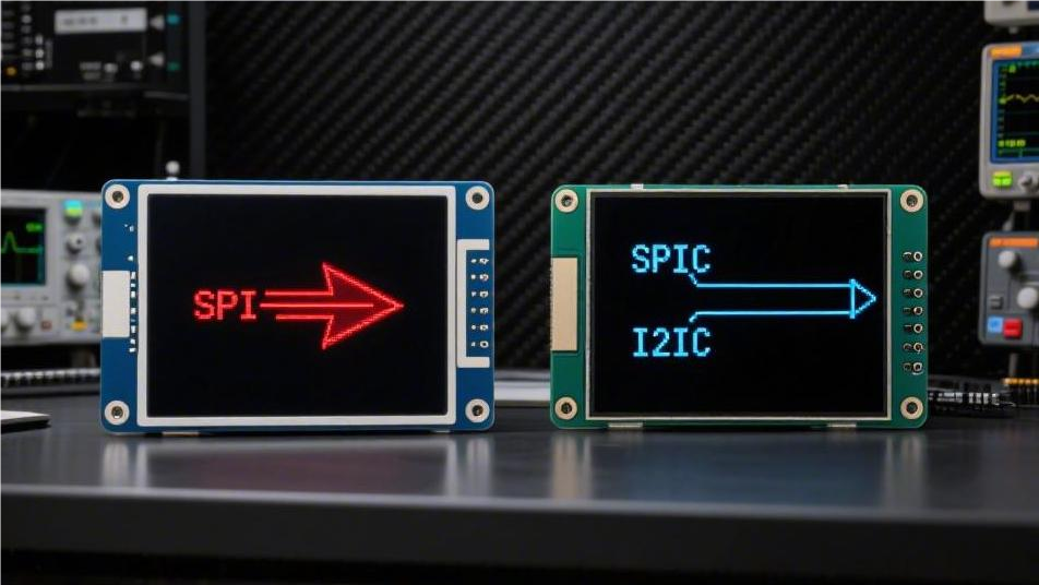
The SPI display interface requires 4 wires and can reach frequencies of 50MHz or higher, making it suitable for driving color TFT screens to smoothly play animations. The I2C interface, on the othe...
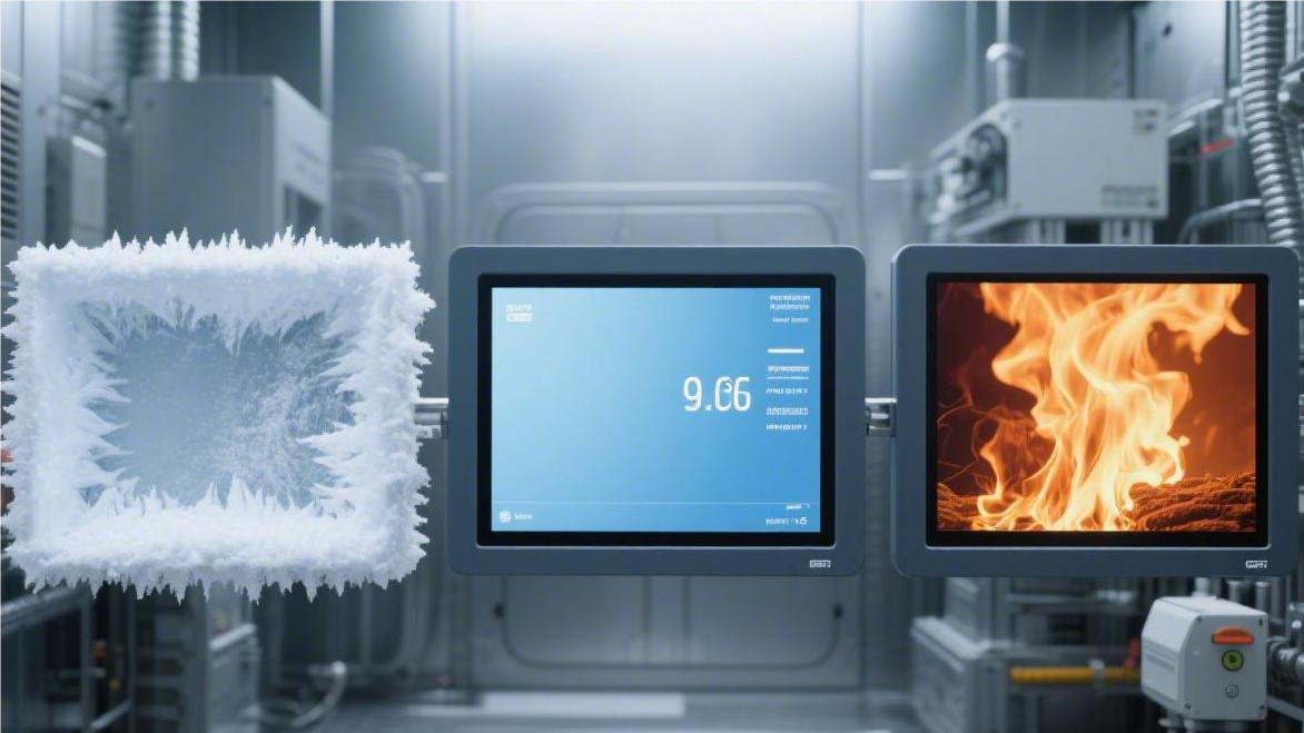
Industrial LCD screen selection must look for the wide temperature standard of -20°C to 70°C. In terms of lifecycle, it is essential to verify data reports showing an MTBF greater than 50,000 hours...
Hinterlasse einen Kommentar
Diese Website ist durch hCaptcha geschützt und es gelten die allgemeinen Geschäftsbedingungen und Datenschutzbestimmungen von hCaptcha.