


OLED Screen Applications | Consumer Electronics, Automotive & VR
Consumer Electronics
Dominates high-end smartphones (e.g., iPhone 15 Pro, 6.1-inch OLED, 500 nits brightness, 98% DCI-P3 color gamut) and TVs (LG C3, 55-inch, peak 2000 nits, million-level contrast ratio).
Thin, light, and low power consumption (20% more power-efficient than LCD), accounting for 70% of the global high-end screen market.
Automotive
Used for instrument clusters/center consoles (Mercedes-Benz EQS Hyperscreen, 56-inch curved OLED, 4560x1920 resolution, temperature resistance -40℃~85℃).
Supports touch + voice interaction, response < 1ms, improving driving information reading efficiency.

VR
The core of headsets (Meta Quest 3, 2160x2160 resolution per eye, 90Hz refresh rate, 1200 PPI pixel density).
Low latency (< 5ms) reduces motion sickness, and 1,000,000:1 contrast ratio enhances immersion.
Consumer Electronics
Consumer electronics account for more than 73% of OLED panel shipments.
On the smartphone side, LTPO 2.0 backplane technology has become a standard configuration, supporting 1Hz-120Hz adaptive refresh rates.
Combined with PWM high-frequency dimming (usually higher than 1920Hz), it effectively solves the flicker eye protection problem.
In the field of TVs and monitors, QD-OLED competes fiercely with WOLED panels equipped with MLA (Micro Lens Array).
This competition has pushed full-screen sustained brightness to over 250 nits and peak brightness past 2000 nits, completely addressing the previous visibility shortcomings of OLED in bright environments.
Additionally, laptop panels have generally reached 100% DCI-P3 color gamut coverage and 0.2ms response speeds.
Smartphones
LTPO Backplane
-
Leakage Current Control
Although LTPS transistors have high electron mobility and fast response, they require constant capacitor refreshing to keep pixels on, resulting in high leakage current. LTPO introduces Oxide TFT components with extremely low leakage current.-
Low-Frequency Maintenance: When displaying static images or text, the screen can drop its refresh rate to 1Hz without fetching new frames from the GPU, refreshing only once per second.
-
Power Consumption Data: This mechanism allows the screen to consume less than 30mW in Always-On Display mode, saving 40%-50% of display power compared to a fixed 60Hz refresh rate.
-
-
Adaptive Sync (VRR)
Modern Display Driver ICs (DDIC) can synchronize frame rates with the phone's processor (SoC).-
Video Playback: Automatically locks to 24Hz, 30Hz, or 60Hz to match the video source frame rate, avoiding the 3:2 pull-down judder that occurs when playing 24fps movies at 60Hz.
-
Gaming Scenarios: Works with the GPU rendering speed to adjust the refresh rate in real-time (e.g., fluctuating between 48Hz-120Hz), eliminating screen tearing.
-
Brightness Management
Brightness is a hard metric for outdoor visibility.
OLED brightness management is divided into three levels:
| Brightness Mode | Brightness Range (nits) | Trigger Condition | Technical Principle |
|---|---|---|---|
| Manual Max Brightness | 500 - 800 | User manually slides to maximum in settings | Limits current to prevent overheating and rapid aging, ensuring luminance uniformity across a full-screen white field. |
| High Brightness Mode (HBM) | 1000 - 1600 | Ambient light sensor detects > 20,000 lux | The system "overclocks" the pixels by increasing voltage. Usually limited in duration (e.g., 10-20 mins) to protect the panel. |
| Local Peak Brightness | 2500 - 4500+ | Playing HDR content with display area < 10% | Concentrates power only on highlight areas (e.g., sun reflections, explosions), utilizing OLED's low APL (Average Picture Level) characteristics. |
-
Micro Lens Array (MLA)
Some top-tier models have begun introducing MLA technology. Billions of micron-sized lenses are covered above the pixel layer to refract light that would otherwise be lost to total internal reflection within the panel. This reduces screen power consumption by 20% at the same brightness, or increases brightness by 20% at the same power consumption.
Dimming Strategy
PWM Dimming Mechanism
The screen doesn't actually "dim"; instead, it deceives the human eye by rapidly alternating between "on" and "off."
The shorter the "on" time and the longer the "off" time, the dimmer the screen appears to the eye.
Flicker Issues
When the PWM frequency is low (e.g., 240Hz or 480Hz), sensitive users may perceive flickering, leading to eye fatigue or headaches.
High-Frequency Eye Protection Solutions
The industry is currently promoting ultra-high frequency PWM of 2160Hz, 3840Hz, or even 4320Hz.
According to the IEEE 1789 standard, there is almost no risk to the human eye when the frequency is higher than 3125Hz.
DC-like Dimming
At the software level, the screen is forced to stay in high brightness mode (DC drive), and the image is dimmed by multiplying the image data with a transparency mask.
While this eliminates flicker, it sacrifices color dynamic range and detail in low grayscale areas.
Home Entertainment
WOLED vs. QD-OLED
-
WOLED (White OLED + Color Filter)
-
Architectural Logic: Vertically stacks blue, yellow, and green organic light-emitting materials to synthesize white light. The light passes through Red, Green, and Blue Color Filters to create colored sub-pixels, with an additional White (W) sub-pixel added to boost brightness.
-
Technical Evolution: The latest Meta Technology introduces "Micro Lens Array" (MLA), integrating billions of micron-sized convex lenses within the panel.
-
Efficiency Boost: MLA solves the total internal reflection issue caused by the refractive index mismatch between the organic material layer and the glass substrate, improving light extraction efficiency by approximately 60%. This means significantly higher brightness at the same power, or significantly reduced heat at the same brightness.
-
-
QD-OLED (Quantum Dot OLED)
-
Architectural Logic: Uses only blue OLED as the backlight. The blue light passes directly through Red and Green Quantum Dot conversion layers. The quantum dots emit high-purity red and green light when excited, while unconverted blue light passes straight through.
-
Color Volume: Since there are no filters blocking the light, QD-OLED maintains extremely high color saturation even at high brightness. It typically reaches around 90% coverage of the BT.2020 color space, significantly better than the 75% of traditional WOLED, making colors more impactful especially in high-brightness red and green scenes (like lava or neon lights).
-
ABL Mechanism
-
APL (Average Picture Level) Curve
-
1% - 10% Window: When displaying very small highlight areas (e.g., the moon in a night sky, explosion sparks), the power supply concentrates energy, allowing brightness to momentarily reach 2000 - 3000 nits.
-
25% - 50% Window: As the emitting area increases, the driver IC linearly reduces voltage, dropping brightness to 600 - 1000 nits.
-
100% Full-Screen White: When the entire screen displays pure white, brightness is strictly limited to between 200 - 300 nits to protect the panel.
-
-
Thermal Subsystem
To break through ABL limits, high-end models attach an aluminum Heatsink or a graphene thermal layer behind the panel. This passive cooling structure allows OLED pixels to maintain high voltage for longer durations, reducing the risk of Image Retention. Test data shows that models equipped with heatsinks last 30% - 50% longer in peak brightness duration than standard models.
Gaming Performance
-
Instant Pixel Response
-
Liquid crystal molecules take time to twist, resulting in Gray-to-Gray (GtG) response times of 3ms - 5ms for LCD screens, causing visual ghosting.
-
The switching process of an OLED pixel is an electrochemical reaction, with response times of only 0.1ms or less. This makes a 60Hz OLED TV appear as clear as a 90Hz LCD TV in terms of motion clarity.
-
-
HDMI 2.1 Protocol Stack
Modern OLED TVs are not just displays, but signal processing centers.-
Bandwidth: Full 48Gbps bandwidth supports 4K 120Hz HDR 4:4:4 uncompressed signal input.
-
VRR (Variable Refresh Rate): Supports G-Sync Compatible and FreeSync Premium Pro. When game frame rates fluctuate between 40fps and 120fps, the screen refresh rate syncs in real-time, completely eliminating tearing and input lag caused by V-Sync.
-
ALLM (Auto Low Latency Mode): When a game signal is detected, the system automatically bypasses video post-processing algorithms (like MEMC), compressing Input Lag to 5ms - 10ms.
-
Lifespan Extension
-
Pixel Shift
The image processor shifts the entire image by 1-2 pixels up, down, left, and right every few minutes. This tiny movement is imperceptible to the eye but effectively prevents fixed icons (like TV logos or game health bars) from lighting up the same set of organic units for too long. -
Static Logo Detection & Local Dimming
The SoC chip has image recognition capabilities to analyze static elements in real-time. Once a bright, static Logo is detected, the system reduces brightness in that local area by about 20% - 40%, while the rest of the dynamic screen remains unchanged.
Compensation Cycle
When the user turns off the TV (standby mode), the system runs a voltage compensation program.
Short Cycle (Every 4 hours)
Scans the TFT backplane for threshold voltage drift and writes compensation data, taking about 5-10 minutes.
Long Cycle (Every 2000 hours)
Performs a deep pixel refresh, detecting areas with uneven aging and adjusting drive current to restore screen brightness uniformity.
IT Equipment
Tandem OLED
In tablets and high-end thin-and-light laptops, single-layer OLEDs struggle to meet both high brightness and long lifespan requirements simultaneously.
Tandem OLED architecture stacks two or more emitting layers (EML) vertically through a Charge Generation Layer (CGL).
-
Voltage and Current Trade-off
-
Double Brightness: At the same current density, the double-layer structure produces double the photon output. This means IT devices can easily reach 1000 nits full-screen brightness in bright outdoor environments without overloading a single emitting material.
-
4x Lifespan: If brightness is kept constant, the driving current can be significantly reduced. Since OLED material degradation speed is proportional to the square of current density, the Tandem structure can theoretically extend panel life by 4 times. This is crucial for IT devices displaying fixed UIs (like browser address bars or taskbars).
-
Energy Optimization: This architecture improves electron transport efficiency, reducing panel power consumption by 30% - 40% at the same brightness, significantly extending laptop battery life.
-
Full-Link Wide Color Gamut
For graphic designers, video editors, and 3D renderers, OLED provides pixel-level light control advantages that traditional IPS panels cannot match.
-
Color Volume
LCD screen colors become washed out as brightness decreases. Due to its self-emissive nature, OLED maintains full color saturation even at extremely low brightness (e.g., 5% brightness).-
Gamut Coverage: Modern OLED IT panels generally cover 100% DCI-P3 (cinema grade) and 95% - 99% Adobe RGB (print grade).
-
10-bit Color Depth: Native support for 10-bit display provides 1.07 billion colors, eliminating color banding in skies or gradient backgrounds compared to 8-bit panels.
-
-
VESA DisplayHDR True Black Standard
HDR standards in the IT field are stricter than for TVs.-
Black Level Standard: To obtain True Black 600 certification, the screen's minimum brightness must be lower than 0.0005 nits. In contrast, even top-tier Mini-LED backlit displays produce blooming when showing small highlight objects like stars due to limited local dimming zones.
-
Pixel-Level Dimming: OLED allows one pixel to show pure white (500 nits) while the adjacent pixel shows pure black (0 nits). This microscopic contrast is essential for checking rendering details.
-
E-sports Monitors
In the desktop monitor space, the refresh rate arms race has pushed OLED to new heights of 480Hz, primarily serving FPS (First-Person Shooter) players.
-
GtG (Gray-to-Gray) Response Time
-
The fastest Fast-IPS panels have response times of about 1ms GtG, often accompanied by severe "Overshoot," causing inverse ghosting at object edges.
-
OLED panels, thanks to their electrochemical luminescence principle, compress response times to 0.03ms. This means pixel color switching is almost instantaneous.
-
-
Motion Clarity
-
Visual tests show that a 240Hz OLED monitor is superior to a 360Hz LCD monitor in motion clarity.
-
This is because LCDs must wait for liquid crystal molecules to twist, while OLED pixels are already in place when each frame refreshes, eliminating physical ghosting and keeping fast-moving crosshairs and enemy outlines sharp.
-
Modern IT OLED panels have broken through the lifespan bottleneck of static displays.
Flagship products generally provide a 1,000,000:1 native contrast ratio and 100% DCI-P3 gamut coverage, with factory-calibrated color accuracy of ΔE < 1, fully meeting Hollywood industrial post-production standards.
Targeting the high energy efficiency needs of mobile computing, the Two-Stack Tandem architecture pushes screen brightness over 1000 nits while reducing power consumption by about 30%.
In the e-sports field, ultra-high refresh rates from 360Hz to 480Hz, combined with 0.03ms (GtG) lightning-fast response, have become the baseline specifications for professional tournaments, completely eliminating motion blur and blooming artifacts during high-speed movement.
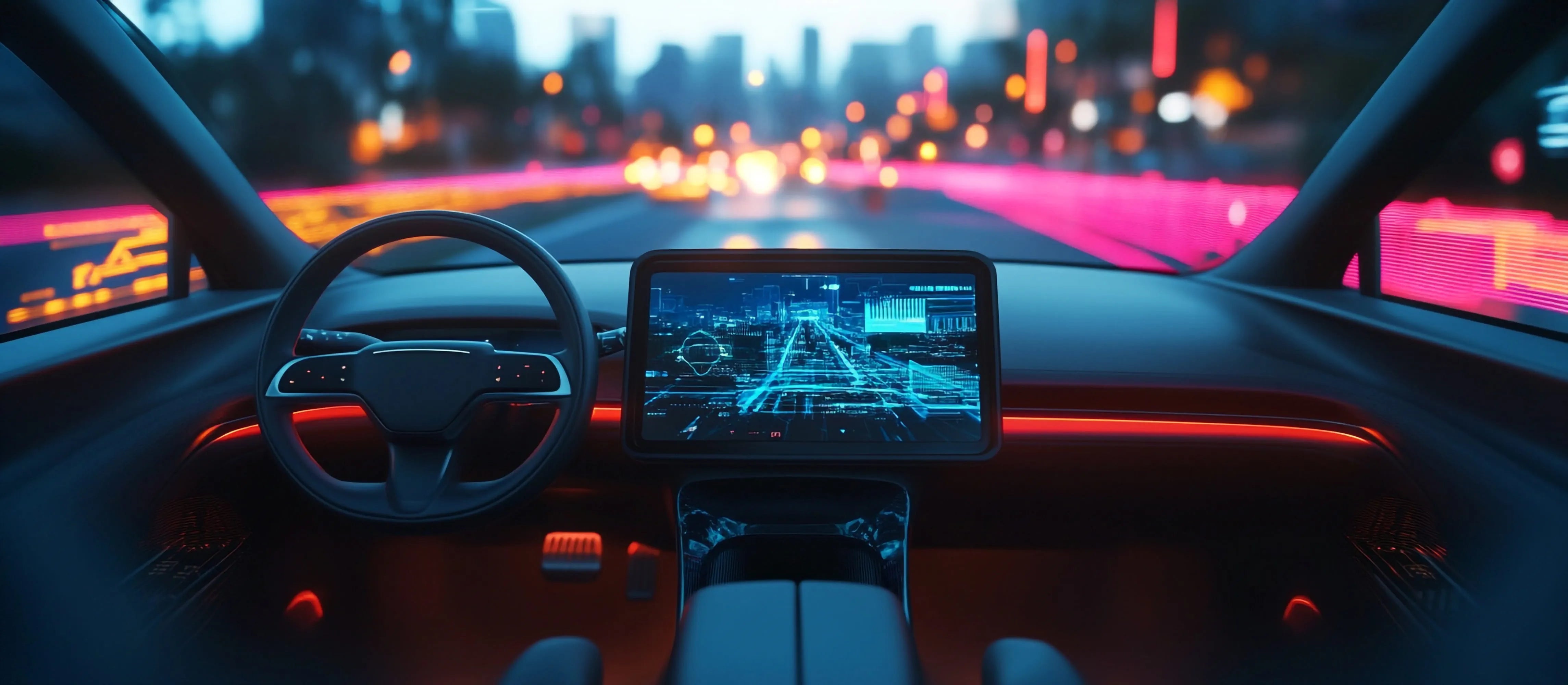
Automotive
According to Omdia data, automotive OLED panel shipments are rising at a compound annual growth rate of 45%, expected to exceed 12 million units by 2027.
To meet the automotive-grade requirement of over 10 years of service life, the industry generally adopts the Two-Stack Tandem structure.
This technology can boost screen brightness to over 1000 nits and extend the life of organic light-emitting materials by 4 times.
Such panels must pass AEC-Q100 certification to ensure that pixel response times remain within 1 millisecond in extreme temperature environments ranging from -40°C to 105°C, completely solving low-temperature ghosting issues.
Currently, LG Display and Samsung Display hold over 90% of this high-end market segment.
Tandem OLED
Physical Architecture
The engineering implementation of the Tandem structure relies on the precise deposition of the Charge Generation Layer (CGL).
-
Internal Construction: A standard Two-Stack Tandem structure consists of "Anode - Hole Transport Layer - First Emitting Layer - Electron Transport Layer - CGL - Hole Transport Layer - Second Emitting Layer - Electron Transport Layer - Cathode."
-
Role of CGL: The CGL is usually a PN junction composed of an N-type layer (supplying electrons toward the anode) and a P-type layer (supplying holes toward the cathode). When voltage is applied, electron-hole pairs are generated within the CGL and injected into the emitting layers on either side.
-
Thickness Control: Despite doubling the emitting layers, the increase in overall panel thickness is only at the micron (μm) level, maintaining the flexible and bendable physical properties of OLED, still capable of fitting automotive dashboard designs with curvature radii smaller than 200mm.
Current Density
Automotive environments demand much higher screen lifespans than consumer electronics (phones have a 2-3 year cycle, cars need 10-15 years).
The decay formula typically follows $T \propto \frac{1}{J^n}$, where $n$ is the acceleration factor (usually between 1.5 and 2.0).
-
Shunting Effect: In a Tandem structure, to reach 1000 nits of brightness, each of the two emitting layers only needs to contribute 500 nits. This means the current flowing through each unit pixel is significantly reduced.
-
Lifespan Gain Calculation: If the current density is halved ($J/2$), according to the acceleration factor calculation, the lifespan isn't just doubled, but extended to 3 to 4 times the original.
-
Blue Material Stability: Blue organic phosphorescent or fluorescent materials are usually the weak link in OLED lifespan. Through double-layer stacking, blue sub-pixels can operate at extremely low loads, thereby avoiding the "blue shift" or rapid burn-in phenomena common at high brightness.
Energy Efficiency Management
Luminous Efficiency (LE) Improvement
Single-layer OLEDs exhibit significant "Efficiency Roll-off" at high brightness, where quantum efficiency drops sharply as brightness increases.
The Tandem structure allows each light-emitting unit to work in the high-efficiency linear region of low brightness, avoiding the roll-off area.
Power Consumption Comparison Data:
| Metric | Single Stack OLED | Two-Stack Tandem OLED |
|---|---|---|
| Drive Voltage | ~4-5 V | ~9-12 V |
| Current Demand (Same Brightness) | 100% (Baseline) | ~30-40% |
| Total Power Consumption | 100% (Baseline) | ~70% (30% reduction) |
| Backplane Heat Loss | High (Significant $I^2R$ effect) | Low (Current significantly reduced, line loss lower) |
Although the voltage increases, because the current drops significantly, the resistive heat loss ($P_{loss} = I^2R$) on the TFT backplane circuits and power lines is substantially reduced, resulting in a 30% reduction in total system-level power consumption.
Extreme Temperatures
Low-Temperature Rheology
-
LCD Physical Bottleneck: Rotational Viscosity
Liquid Crystal Displays (LCD) rely on voltage-driven physical rotation of liquid crystal molecules to control light passage. As a fluid, liquid crystal material's viscosity ($\gamma$) follows a variant of the Arrhenius Equation. When temperature $T$ drops, viscosity rises exponentially.-
At 25°C room temperature, the rotational viscosity of nematic liquid crystals is low, with response times around 10-20ms.
-
At -20°C, the increased viscosity leads to a massive surge in mechanical resistance for molecular rearrangement, extending response times to 200ms.
-
At -40°C, some liquid crystal materials approach their freezing point, and response times may exceed 500ms. This means the screen can only refresh 2 frames per second, resulting in images that aren't just ghosting, but completely "frozen" or fragmented.
-
-
OLED Physical Advantage: Carrier Injection
OLED (Organic Light Emitting Diode) is an all-solid-state device. Its light-emitting principle is based on the injection, transport, and recombination of electrons and holes in organic semiconductor layers.-
Electron Mobility: Although organic material carrier mobility ($\mu$) slightly decreases as temperature drops, the magnitude of change is far smaller than that of fluid viscosity.
-
Photophysical Process: Exciton formation and radiative decay processes occur at the nanosecond (ns) to microsecond (\mu s) level. Even at -40°C, OLED pixel turn-on and turn-off times remain controlled at 0.1ms or less.
-
ISO 16505 Standard
Low-Temperature Response Time Comparison Data (Gray-to-Gray GtG):
| Ambient Temperature | Automotive IPS-LCD Response Time | Automotive OLED Response Time | Visual Perception Result |
|---|---|---|---|
| 25°C | 25 ms | < 0.1 ms | Both are smooth; OLED has higher motion clarity. |
| 0°C | 60 ms | < 0.1 ms | LCD shows slight edge blur; OLED remains sharp. |
| -20°C | 250 ms | < 0.2 ms | LCD shows long trails in dynamic images; unable to identify details of moving objects. OLED unchanged. |
| -30°C | > 450 ms | < 0.2 ms | LCD image lags severely; obstacle positions displayed incorrectly when reversing. OLED works normally. |
-
Removal of Cold-Start Heaters: To solve LCD low-temperature lag, traditional automotive screen modules must integrate a transparent heater (ITO Heater) to preheat the panel. This not only adds 10-15% energy consumption but also increases module thickness and optical transmission loss. OLED, with its native low-temperature capability, requires no auxiliary heating components, directly reducing system complexity and cold-start power consumption.
Brightness Decay
When a car is exposed to the summer sun outdoors, the greenhouse effect in a closed cabin can cause dashboard surface temperatures to climb rapidly to 80°C - 100°C.
1. Isotropic Phase Transition (Clearing Point)
Liquid crystal materials, upon reaching a specific critical temperature (Clearing Point), transition from an ordered liquid crystal state to a disordered isotropic liquid state.
-
LCD Failure Mode: Once the clearing point is exceeded (usually 90°C-100°C for automotive grade), liquid crystal molecules lose their ability to control light polarization, and the screen becomes a black, unviewable patch in parts or as a whole.
-
OLED Stability: OLED materials have no such phase transition mechanism. Automotive-grade organic light-emitting materials are thermally improved, with glass transition temperatures (Tg) usually designed above 120°C. In 105°C extreme tests, OLEDs continue to display images normally without physical phase transition failure.
2. Brightness Maintenance at High Temperatures
High temperatures accelerate material aging and reduce luminous efficiency.
-
Thermal Quenching: At high temperatures, the probability of non-radiative recombination (generating heat instead of light) increases.
-
Compensation Mechanism: Modern automotive OLED driver ICs (DDIC) have built-in temperature sensors. When panel temperature rise is detected, algorithms adjust drive current (Current Compensation) in real-time to maintain the set brightness (e.g., 800 nits). While this temporarily increases power consumption, it ensures screen content remains clearly visible in high-temperature, direct sunlight scenarios. Tests show that after running continuously for 500 hours at 85°C, the brightness decay of Tandem OLED can be controlled within 3%.
P-OLED and Free-form Design
PI Process
-
Liquid Film Formation: The manufacturing process begins by coating liquid polyimide varnish onto carrier glass. This material must withstand a 400°C - 450°C high-temperature curing process to form a transparent or pale yellow film only 10 - 20 microns (μm) thick.
-
TFT Array Construction: On the cured PI layer, LTPS (Low-Temperature Polycrystalline Silicon) or Oxide thin-film transistor arrays are built using photolithography.
-
Laser Lift-Off (LLO): This is the step that differentiates it from rigid OLED. Once all organic emitting and encapsulation layers are deposited, a high-energy UV laser beam scans from the glass side. The laser energy breaks chemical bonds at the PI-glass interface, releasing gas and allowing the flexible PI panel to be stripped from the rigid carrier glass without damage.
Multi-Dimensional Curves
Automotive interior design P-OLED breaks through the two-dimensional plane, allowing the display to bend along multiple axes to adapt to the complex, streamlined surfaces of a vehicle's interior.
| Design Form | Technical Parameters | Application Scenario |
|---|---|---|
| Single-Axis Concave Curve | Curvature Radius R800mm - R3000mm | Surrounds the driver's main instrument cluster, providing an immersive perspective and shortening line-of-sight focus distance. |
| S-Curve | Combines concave and convex designs | Integrated center console screen connecting to the passenger screen, shaped in waves according to the ergonomic contours of the console. |
| Edge Bending | Bending angle close to 90° | Side-view displays or instrument edges, eliminating blind spots and achieving a borderless visual effect. |
Difference between Cold Bending and Hot Bending:
LCDs can also be made curved, but they usually require Hot Forming of the glass, which has low yield and is prone to stress causing Mura (light leakage).
P-OLED's PI substrate is naturally flexible and can undergo Cold Forming during the module assembly stage, ensuring optical consistency of the panel without changing pixel aperture ratio or causing color mixing due to bending.
Weight Reduction
In Electric Vehicle (EV) engineering, display system weight is often underestimated.
Traditional LCD modules over 30 inches, plus backlight units and glass covers, can weigh several kilograms.
-
Density Difference: Glass density is about 2.5 g/cm³, while polyimide is about 1.4 g/cm³.
-
Structural Simplification:
-
Removal of Backlight Module: Eliminates Light Guide Plates (LGP), brightness enhancement films, diffusers, and metal backplates.
-
Substrate Thinning: Rigid OLED glass substrates are usually 0.5mm x 2 (TFT + encapsulation), while P-OLED's PI substrate is only 0.01mm - 0.02mm.
-
Cover Glass Optimization: While P-OLED still requires a protective cover glass, because the panel itself is flexible, thinner chemically strengthened glass or composite polymer covers can be used.
-
For a 40-inch integrated display system spanning the entire dashboard, using P-OLED can reduce weight by 1.5kg to 2.5kg compared to an LCD solution.
According to automotive engineering formulas, a vehicle weight reduction of 10kg is roughly equal to a 1% increase in range or a 1g/km reduction in CO2 emissions;
P-OLED's contribution here is quantifiable.
VR
Currently, high-end VR hardware display standards are shifting from Fast-LCD to Silicon-based OLED (Micro-OLED/OLEDoS).
Unlike traditional glass-substrate OLEDs, which are limited to about 600 PPI due to the FMM process, OLEDoS uses CMOS semiconductor processes to boost pixel density to over 3000 PPI.
Per-eye resolution can reach 4K, bringing angular resolution (PPD) close to the human eye's retinal limit (60 PPD).
Furthermore, OLED features microsecond-level response speeds of < 0.1ms, which, combined with 10% duty cycle black frame insertion, eliminates motion blur.
To counter the only ~10-15% light efficiency of Pancake optical paths, the brightness of the latest Tandem Micro-OLED panels has exceeded 5000 nits, ensuring the light reaching the eye remains in the comfortable 100-200 nits range.
Micro-OLED
Manufacturing Process
CMOS Driving Backplane
-
Wafer Selection: Production typically uses 8-inch or 12-inch monocrystalline silicon wafers. Compared to the LTPS or IGZO used on glass substrates, monocrystalline silicon has electron mobility several orders of magnitude higher.
-
Process Node: Driving chips are usually manufactured using mature CMOS process nodes from 28nm to 180nm. The choice here isn't extreme computing speed, but rather the ability to withstand the high voltages (usually 5V - 10V) required for OLED driving and ensuring high pixel consistency.
-
Pixel Circuitry: All driving circuits (pixel switches, capacitors, voltage compensation circuits) are integrated inside the silicon substrate, directly beneath the emitting pixels. This "Top Emission" structure ensures that pixel aperture ratios are unaffected by circuit wiring, maintaining sufficient emitting area even for tiny pixels.
Front-End Emitting Layer Deposition
-
Anode Preparation: Reflective anodes (usually aluminum or silver alloy) are prepared on the silicon wafer. This metal layer acts as both an electrode and a mirror, reflecting light upward.
-
Vacuum Evaporation: In a high-vacuum environment, organic materials are deposited layer-by-layer onto the wafer via thermal evaporation. Since pixel sizes are below the physical limits of traditional FMM (Fine Metal Mask), Micro-OLEDs cannot be physically masked for each sub-pixel and thus usually use full-surface evaporation.
Pixel Structure
WOLED + CF (White + Color Filter)
-
Luminescence Principle: Vertically stacks red, green, and blue emitting materials (or complementary color materials) so every pixel emits white light.
-
Color Filtering: Above the white OLED layer, R, G, and B color filter layers are prepared directly using semiconductor photolithography.
-
Efficiency Data: The downside of this approach is light loss. Color filters absorb about 2/3 of the light, leading to a significant drop in luminous efficiency. To compensate for brightness, the driving current for the organic material must be greatly increased.
dPd RGB (Direct Patterned RGB)
-
Maskless Lithography: Uses photoresist to pattern OLED materials directly, or uses Silicon Shadow Masks instead of traditional metal masks.
-
Efficiency Advantage: Theoretically, the RGB independent emission structure is 3 to 4 times more brightness-efficient than the WOLED+CF solution and offers wider gamut coverage (over Rec.2020 90%).
-
Technical Barrier: Precisely depositing three materials at the micron scale is extremely prone to color mixing or organic material degradation. Currently, only a few US and Japanese manufacturers (like eMagin) possess small-scale mass production capabilities.
Brightness Enhancement Technology
Tandem Stacked Structure
-
Structural Principle: Vertically stacks two or more EL Units connected by a Charge Generation Layer (CGL).
-
Voltage and Current: At the same current density, a Two-Stack Tandem structure is twice as bright as a single layer; or it produces the same brightness at half the current density.
-
Lifespan Extension: Since OLED lifespan is inversely proportional to the square of current density, reducing current density can extend device life by more than 4 times. High-end Micro-OLEDs now commonly use double or even triple-stack Tandem structures.
MLA (Micro Lens Array)
-
Physical Layer: An array of billions of micron-sized convex lenses is fabricated above the color filter.
-
Path Alteration: These microlenses change the exit path of light, extracting light that would otherwise be trapped inside the device due to total internal reflection and focusing it forward.
-
Gain Data: MLA technology can boost center brightness by 20% to 40% without increasing power consumption.
Despite rising Micro-OLED efficiency, integrating millions of light points on a 1-inch area results in massive heat density.
Mass production standard sizes are currently concentrated in 0.49-inch (for EVFs), 1.03-inch (square VR panels), and 1.3/1.4-inch (high-end VR/MR panels).
Wafer cutting efficiency determines cost; the utilization rate for a 1.3-inch panel on a 12-inch wafer is much lower than for a 0.49-inch panel, causing the cost of large Micro-OLEDs to rise exponentially.
Dynamic Response
Response Time
Physical Viscosity of Liquid Crystal (LCD)
-
Twist Mechanism: LCDs rely on voltage to physically rotate liquid crystal molecules to change transparency. This is a mechanical process limited by fluid viscosity and molecular weight.
-
Overdrive Limits: Although Fast-LCD uses Overdrive voltage to speed up molecular twisting, compressing GtG response times to about 4ms, this is near the physical limit of the materials.
-
Temperature Sensitivity: LCD viscosity increases significantly as temperature drops. In cold environments, LCD response times can lengthen several-fold, causing severe ghosting, whereas VR devices often need to adapt to different ambient temperatures.
Electronic Transition of OLED
-
Luminescence Mechanism: OLED is a solid-state electronic device where holes and electrons combine in the emitting layer to create excitons and radiate photons.
-
Microsecond Response: This process involves only electronic energy level transitions, without macroscopic physical movement. Typical response times for Micro-OLED are less than $0.01ms$ (10μs).
-
Synchronicity: This nearly instantaneous response means pixel color changes are perfectly synchronized with the GPU's frame output signals, eliminating physical latency accumulation at the display end.
Persistence
The Issue with Sample-and-Hold
Traditional displays (including most phones and monitors) keep pixels lit throughout the refresh cycle.
-
Scenario: A user turns their head to the right; their eyes reflexively turn left to keep focus on a virtual object (Vestibulo-Ocular Reflex).
-
Blur Cause: If the screen refreshes at 90Hz, each frame displays for $11.1ms$. During this 11ms, the human eye is scanning/moving while the image remains fixed in position. Consequently, the image slides across the retina, causing Motion Blur.
Low Persistence Solution
The ultra-fast switching of OLED allows it to perform "Impulsive Display."
-
Duty Cycle: At a 90Hz refresh rate, the OLED panel doesn't stay lit for the full 11ms. It might only light up for the first 1ms or 2ms and then immediately turn off (displaying black) for the remaining 9ms.
-
Persistence of Vision: Because the light duration is so short, the image left on the retina is just a momentary, sharp impression. The brain uses persistence of vision to fill in the 9ms dark gaps.
-
Quantification: At a head rotation speed of $100^\circ/s$, a full-persistence display (11ms) would smear an object edge by about 1.1 degrees; with a 10% duty cycle (1ms light), the blur is only 0.1 degrees, below the human detection threshold.
BFI
Brightness Compensation Algorithm
-
Duty Cycle Dilemma: If light duration is cut from 100% to 10%, perceived average brightness drops to 1/10 if intensity remains the same.
-
Peak Brightness Requirement: To see a comfortable 150 nits, the OLED panel's physical brightness during that 1ms pulse must actually reach 1500 nits. If considering the 90% light loss of Pancake lenses, the peak brightness requirement at the panel source surges past 15,000 nits.
-
Necessity of Tandem: This explains why Two-Stack or Three-Stack Tandem OLED is a must for VR. Single-layer OLEDs would age rapidly under such high pulse currents, but multi-layer structures distribute the current density, making this extreme strobe driving possible.
Black Smearing
Despite fast response times, a specific physical artifact called Black Smearing occurs when switching from "pure black" (0) to "dark gray" (1-5).
Cause Analysis
-
Turn-on Threshold: It takes time to charge OLED pixel capacitors to the Threshold Voltage. When starting from a completely off state (0V), the charging rate is slower due to weak current at low voltages.
-
Visual Manifestation: When moving gray objects in dark scenes, purple or black trails are left behind the object.
Engineering Fixes
-
Mura Compensation & Voltage Pre-setting: Modern Micro-OLED DDICs use a strategy where pixels are never completely turned off.
-
Grayscale Floor: "Black" is defined as a very low-brightness dark gray (e.g., 0.001 nits), keeping pixels in a sub-threshold conduction state.
-
Result: While this sacrifices an infinitesimal amount of contrast (not absolute 0 nits), it eliminates capacitor charging delays, ensuring dark-field transitions are as fast as bright-field ones.
The physical basis for VR immersion lies in keeping Motion-to-Photon (MTP) latency strictly under 20ms.
OLED technology, via its current-driven mechanism, achieves pixel response times (GtG) of $<0.1ms$, a magnitude better than the 4-5ms physical limit of Fast-LCD.
This speed allows displays to use a Low Duty Cycle (10% or less) driving mode, compressing light duration to 1-2ms per frame via Black Frame Insertion.
This Low Persistence strategy utilizes the human eye's persistence of vision to keep motion blur within 1 pixel even when the user rotates their head at $100^\circ/s$.
Brightness
Physical Cost
To move away from the "brick-like" bulk of early VR headsets, optical solutions shifted from aspherical Fresnel lenses to folded optics (Pancake).
Polarized Folding Principle
Pancake modules rely on light folding back and forth within the lens group to extend the optical path within a short physical distance.
This depends heavily on polarization control:
-
Beam Splitter (BS): OLED light first passes through a splitter; 50% passes, 50% is reflected (lost).
-
Quarter-Wave Plate (QWP): Light passes through the plate, converting linear polarization to circular polarization.
-
Polarizing Beam Splitter (PBS): Uses polarization selectivity to reflect light back to the BS.
-
Second Fold: Light passes through the QWP and BS again, finally entering the eye.
System-Level Light Loss Calculation
Every "fold" comes with a physical energy reduction.
-
Transmission Loss: Passing through a 50/50 splitter twice leaves only 25% energy.
-
Polarization Loss: Absorptivity and non-ideal transmittance of polarizers further devour light.
-
Medium Absorption: Internal absorption by multi-layer resin or glass lens materials.
Combined, standard Pancake module Light Efficiency is only $10% - 13%$.
In contrast, traditional Fresnel lenses have an efficiency of $85% - 90%$.
This means Pancake solutions require 7 to 8 times the screen brightness to achieve the same brightness at the eye.
Budget Equation
The Mandatory 10% Duty Cycle Constraint
As mentioned, to eliminate Persistence blur, VR screens use pulse displays.
-
Time Window: At 90Hz, each frame is lit for about $1.1ms$ (10% duty cycle), with $10ms$ of black.
-
Perceived Brightness: Human brightness perception is a result of time integration. If instantaneous brightness is $L_{peak}$, then $L_{eye} \approx L_{peak} \times 10%$.
Peak Brightness Deduction
Assuming the goal is to replicate indoor reality (approx. 150 nits) at the eye, with Pancake efficiency (set at 12%) and duty cycle (10%), the required source brightness $L_{source}$ is calculated as:
$$ L_{source} = \frac{L_{eye}}{Efficiency_{optical} \times DutyCycle} = \frac{150 \text{ nits}}{0.12 \times 0.10} = 12,500 \text{ nits}$$
This explains why standard phone OLEDs (< 2000 nits) are entirely unsuitable for Pancake VR.
Micro-OLEDs must function as miniature searchlights.
Tandem Structure
In single-layer OLEDs, brightness is proportional to current density.
Reaching 10,000+ nits requires massive current injection.
This causes organic materials to generate Joule heat rapidly, leading to Thermal Roll-off and permanent burn-in.
Double and Triple-Stack Architectures
Tandem structures solve this physically by stacking multiple EL Units vertically.
-
Charge Generation Layer (CGL): Between emitting units, a CGL of N-type and P-type materials generates electrons and holes under an electric field for the layers above and below.
-
Quantum Efficiency Multiplication: One electron passing through a Tandem structure can trigger two or three consecutive photon radiations. This means at the same current, a double-stack is twice as bright as a single layer.
-
Voltage Cost: This efficiency comes at the price of stacked drive voltage. While single-layer OLEDs need 4-5V, a double-stack needs 8-10V. However, HV CMOS processes in silicon backplanes can handle this maturely.
Lifespan Dividend
Tandem's true value is in lifespan.
-
Reverse Thinking: To maintain the same brightness, a double-layer structure needs only half the current density of a single layer.
-
Decay Model: OLED decay speed is proportional to the 1.5 to 2nd power of current density. Halving current can extend theoretical life by 3 to 4 times—crucial for VR devices often displaying high-brightness imagery.
MLA
Total Internal Reflection Trap
In traditional OLEDs, since organic and encapsulation glass indices ($n \approx 1.5$) are higher than air ($n=1$), much light undergoes total internal reflection, trapped inside and turning into heat.
Standard OLED light extraction is only about 20%.
Introduction of Micron Lenses MLA technology uses photolithography to create an array of billions of micron-sized hemispherical lenses above the color filter.
-
Path Correction: Microlenses change the critical angle, "pulling" light out that would otherwise reflect back.
-
Beam Shaping: For VR, MLA can be designed to concentrate light within the Pancake lens Eye Box, reducing wasted scatter.
With MLA, Micro-OLED axial brightness can increase by $20% - 40%$ without added power or heat.
Weiterlesen
Automotive OLED utilizes flexible substrates to bond with curved dashboards, meeting automotive-grade temperature resistance standards of -40°C to 105°C. HUDs employ Transparent OLED (transmittance...
OLED screens are usually covered with reinforced glass with a Mohs hardness of over 6 to resist scratches. To prevent uneven aging of organic emitters causing burn-in, always enable the "Pixel Shif...
Hinterlasse einen Kommentar
Diese Website ist durch hCaptcha geschützt und es gelten die allgemeinen Geschäftsbedingungen und Datenschutzbestimmungen von hCaptcha.