


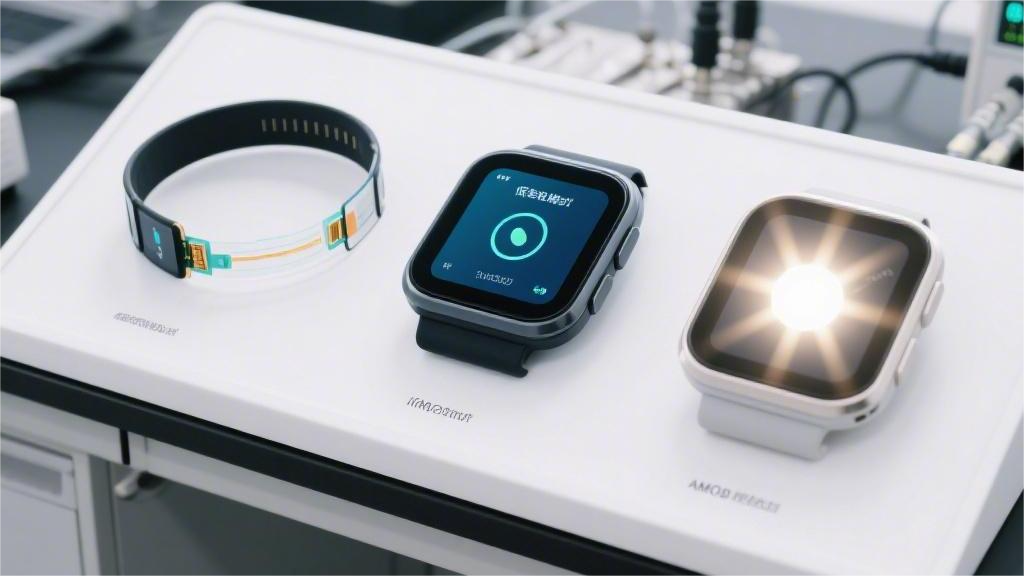
Custom PMOLED Solutions | Tooling Cost, Shape Options
The tooling cost for a custom PMOLED is approximately $2,000 to $5,000, supporting circular or custom-shaped cutting.
During operation, a CAD drawing containing the FPC pins and display area dimensions must be submitted, along with the selection of an SSD1306 driver IC. After layout confirmation, the first version of samples can be delivered in about 3 to 4 weeks.
Tooling Cost
Semi-customization, which only modifies the FPC shape or pins, costs between $1,500 and $3,000 and takes 2-3 weeks.
Reconfiguring the glass substrate size or resolution is considered full customization and requires remaking the ITO glass photomask. The cost rises to $5,000-$10,000, with a cycle of 4-6 weeks.
When the cumulative purchase volume of a single model reaches 50,000 to 100,000 pieces, manufacturers usually offer a full NRE (Non-Recurring Engineering) refund policy.
NRE Cost Composition
In the initial engineering expenditures for custom PMOLED displays, the manufacturing of the photomask accounts for the largest proportion of capital outlay. The factory completes the evaporation of the ITO (Indium Tin Oxide) conductive layer and organic light-emitting materials in a cleanroom, which heavily relies on high-precision metal masks. A 1.5-inch monochrome panel supporting a 128x64 resolution requires the production of 3 to 5 different photomasks.
-
For manufacturing a panel with a 0.15mm dot pitch, the laser cutting error of the photomask is limited to within ±2 micrometers.
-
Using the FMM (Fine Metal Mask) process to achieve a higher PPI (Pixels Per Inch), such as a display density of 200 PPI, will incur an additional $800 to $1,200 in manufacturing costs per mask.
-
The insulator layer and metal cathode layer inside the panel also incur independent tooling charges.
-
Segment OLEDs that only display numbers or simple icons require only 1 or 2 photomasks due to their simple graphics, reducing the total cost to between $1,500 and $2,000.
After the display panel is encapsulated, the Flexible Printed Circuit (FPC) is responsible for connecting the screen to the motherboard. FPC prototyping constitutes the second expense on the engineering bill. Engineers need to export Gerber files using AutoCAD, which include routing layout, pin assignment, and the location information of the stiffener.
-
FPC tooling includes the production of punching dies and cutting dies, with basic processing fees ranging from $800 to $1,500. Using the common 0.5mm pitch ZIF socket standard, the cutting die tolerance is set to ±0.05mm.
-
When the pin pitch is reduced to high-density arrangements of 0.3mm or even 0.2mm, ordinary punching dies are replaced by high-precision laser cutting machines, increasing the cost by $400 to $600.
-
Designs requiring Surface Mount Technology (SMT) for extra capacitors or step-up circuits on the FPC also incur a processing fee for solder paste stencils, which is about $150.
After hardware assembly is completed, power-on lighting tests must be conducted using a dedicated fixture. The manufacturing cost of the Testing Jig is listed separately on the bill. Based on the customized FPC pin drawings, the factory processes a base using acrylic or bakelite boards and installs gold-plated pogo pins on it.
The number of probes equals the number of FPC pins. A testing jig with 24 pins costs between $300 and $500. Software engineers will also spend time writing matching Initialization Code. If a non-standard driver IC is used (e.g., replacing SSD1309 with SSD1327) or the row/column pixel structure of the panel is adjusted (e.g., changing from 128x64 to 128x96), the register setup parameters need to be reconfigured.
The original manufacturer charges a software debugging fee of $300 to $600 to ensure the panel presents the correct Gamma curve and contrast under different voltage domains (such as 3.3V or 5V). Some industrial-grade wearable devices require a layer of Corning Gorilla Glass to be laminated on the PMOLED surface as a protective cover lens. Customizing this cover glass, with a thickness of 0.55mm to 1.1mm, requires making special CNC profile cutting dies and silk-screen meshes.
For a 2.0-inch cover lens with chamfers and a black silk-screened border, the combined CNC setup fee and mesh production fee are approximately $1,200 to $1,800. If the solution further integrates a Projected Capacitive (PCAP) touch screen, a tooling fee for the Sensor pattern will be added to the NRE bill. The customization of the ITO Sensor film is similar to the display photomask but involves fewer layers, with processing fees ranging from $2,000 to $3,500.
The firmware for the touch control IC (such as FocalTech or Goodix) needs to recalibrate sensitivity according to the size and thickness of the touch panel, incurring a firmware debugging fee of about $500.
| NRE Project Category | Included Specific Engineering Components | Data and Dimensional Details | Price Range (USD) |
|---|---|---|---|
| Display Panel | ITO conductive layer mask, organic layer mask, cathode metal mask | 0.15mm dot pitch, ±2μm laser cutting error, 200 PPI density | $4,500 - $7,000 |
| Flexible Circuit | FPC profile cutting die, Surface Mount Technology (SMT) stencil | 0.5mm/0.3mm pin pitch, ±0.05mm tolerance requirement | $800 - $1,500 |
| Testing Jig | Acrylic/bakelite base, gold-plated Pogo Pin array | Matches 24-Pin to 40-Pin interface, 3.3V/5V voltage environment | $300 - $500 |
| Cover Lens & Touch | CNC profiling die, silk-screen mesh, ITO Sensor film | 0.55-1.1mm cover thickness, PCAP firmware sensitivity calibration | $3,700 - $5,800 |
| Software Engineering | Driver IC register parameter config, Gamma curve & contrast tuning | Initialization code adapted for ICs like SSD1309/SSD1327 | $300 - $600 |
By adding multiple independent tooling charges together, the initial NRE bill for a complete PMOLED solution—including a custom panel, custom-shaped FPC, and silk-screened cover lens—can total between $8,500 and $12,000. Upon receiving this budget, factory engineers will procure raw materials and schedule production. From drawing confirmation to the delivery of the first batch of 10 to 15 Engineering Samples (ES) to your lab in Munich or Boston, the timeframe is usually 4 to 5 weeks.
After sample delivery, the project enters the Design Verification Test (DVT) phase. Testers will operate the panel in an environment of 85°C high temperature and 85% relative humidity for 240 hours to check the sealing performance of the UV glue encapsulation around the panel. If black spots (black screen shrinkage phenomenon) appear at the edges of the screen during this stage, factory engineers will modify the encapsulation process drawings and remake the pressing fixture.
Full Customization & Semi-Customization
The industry benchmark quotation for a standard 0.96-inch 128x64 resolution PMOLED panel is approximately $1.20. When an industrial design team in California reserves a non-standard display window on a 3D-printed casing, the R&D team must conduct financial calculations regarding the NRE budget and product lifecycle.
The manufacturing plant does not need to reprocess expensive glass photomasks; they simply extract ready-made glass stock from constant-temperature drying cabinets. The hardware engineers' focus entirely shifts to the FPC routing layout so that the ribbon cable can accurately match the physical location of the connector on the motherboard.
-
The physical length of the FPC is extended or shortened, with tolerances controlled within ±0.2mm.
-
Motherboard pin pitch is compressed from the standard 0.5mm to 0.3mm.
-
Communication protocol rewrites pin mapping from SPI to an I2C interface.
-
ZIF plug-in tail is changed to Hot Bar Soldering.
-
SMD decoupling capacitors in 0402 packages are added to the ribbon cable.
Implementing the aforementioned FPC physical shape modifications typically results in a factory bill maintained between the $1,500 and $2,500 range. Silicon Valley hardware startups frequently adopt this engineering approach during agile development phases. Production line engineers create new cutting dies and testing jigs, and the delivery cycle for the first 20 engineering samples can be compressed to within 2 to 3 weeks.
Faced with entirely new industrial ID design requirements—such as a blueprint specifying a non-standard 1.13-inch panel with a 128x96 resolution—the original standardized glass substrate cannot undergo secondary physical cutting. The engineering pipeline reverts to base physical layer manufacturing, fully initiating a full customization production flow.
The factory prepares and coats organic light-emitting materials anew in a Class 100 cleanroom. Panel engineers draw complete photomask blueprints in AutoCAD, encompassing the Active Area, routing area, and Bonding Area. If the pixel dot pitch of a monochrome panel is set to 0.18mm, the laser cutting error compensation must be precisely calculated down to the micrometer level.
-
Non-standard resolution setting matrices, such as 132x64 or 96x96.
-
Special physical dimensions cutting, like a 1.05-inch rectangle.
-
Irregularly shaped substrates requiring CNC profile cutting, such as circles or octagons.
-
Off-center placement of the light-emitting pixel area on the glass substrate.
-
Customizing specific light-emitting wavelength materials, for instance, 470nm pure blue light.
Re-preparing the ITO conductive glass mask and metal cathode photomask will drive the initial NRE bill up to between $5,000 and $9,000. The evaporation production line allocates 4 to 6 hours of equipment calibration and cleaning time for the new tooling. From the moment the technical specifications (Spec) are signed into effect until the first batch of prototypes arrives at the Frankfurt lab, the time span stretches up to 5 to 6 weeks.
Changes to the physical dimensions of the glass substrate synchronously trigger a replacement in the main driver IC selection. The SSD1306 master chip originally used to drive 128x64 pixels must be upgraded to an SSD1327 or SH1107 supporting higher row scanning when faced with a 128x96 pixel matrix. Changing the IC not only alters the COG (Chip on Glass) bonding parameters but also demands refactoring the software's register initialization code.
Firmware engineers measure the VCOMH voltage values at different ambient temperatures in the lab to ensure the panel's overall operating current consumption under 100 nits display brightness remains strictly below 15mA. Before leaving the factory, non-standard customized panels undergo reliability verification far more rigorous than standard products.
-
120 hours of continuous accelerated aging in an 85°C high-temperature environment.
-
Cold start and refresh rate response testing in a -40°C low-temperature environment.
-
ESD contact discharge tolerance testing of ±4kV for exposed pins.
-
Z-axis mechanical vibration frequency sweep verification from 10Hz to 55Hz.
When the finance department evaluates early customization plans, the Minimum Order Quantity (MOQ) serves as a rigid engineering constraint. Semi-custom projects usually require a minimum purchase of 3,000 pieces per production run to amortize the setup fees for SMT placement machines and test instruments. Full custom projects involve cutting and layout scheduling for the Mother Glass, with a single production run yielding at least 5,000 to 10,000 finished units.
CAM engineers on the manufacturing side optimize the layout of a 370mm x 470mm Generation 2.5 Mother Glass; a single mother sheet can yield approximately 1,200 custom 1.5-inch screens. By optimizing the scrap margin rate along the edges, the material cost per finished unit is further reduced by $0.15.
The hardware team pays the upfront NRE bill during the Engineering Verification Test (EVT) phase. Once the product progresses as planned and enters the Mass Production (MP) phase of 100,000 units within its lifecycle, the manufacturer fully refunds the initial tooling cost according to the commercial terms of the procurement contract.
European industrial control equipment manufacturers tend to use lower-cost semi-custom FPC solutions for their first-generation products. When shipment forecasts for second-generation hardware clearly exceed 50,000 units, they then fully adopt custom glass substrates tailored to the casing structure. Staggering R&D investments balances BOM material cost constraints with the engineering progress demands of Time-to-Market.
Tooling Cost Refund
When a hardware enterprise pays an $8,500 full-custom NRE bill to a display manufacturer, a full refund agreement is attached to the procurement contract. An industrial instrument manufacturer in Munich, when planning a 1.3-inch PMOLED project, accounts for this fee as an early R&D sunk cost. When cumulative off-take for the single custom panel crosses the financial red line of 100,000 pieces, the factory initiates a full refund process.
The establishment of the refund threshold is strictly tied to the single-piece Bill of Materials (BOM) quote of the custom screen. For a 1.5-inch monochrome OLED panel with a factory price of $1.45, the NRE refund target is typically set at 80,000 pieces. If the panel integrates a PCAP capacitive touch layer, the unit price rises to $3.20. Because the profit margin per unit increases, the refund threshold is correspondingly lowered to 50,000 pieces.
Smart home hardware teams in Silicon Valley often use tiered refund terms in their financial calculations to alleviate cash flow pressure during the startup phase. When the first mass-production order reaches 25,000 pieces, the supplier will issue a Credit Note in the amount of $4,250.
This credit note effectively refunds 50% of the photomask processing fee. The remaining 50% balance is settled over the next 12 months alongside the delivery of another 25,000 pieces ordered. Tiered operations dramatically reduce the buyer's inventory risk and cash flow burden.
In cross-border financial settlements, manufacturers rarely use international wire transfers to send cash back to a customer's Boston bank account. The standard engineering financial practice is to convert the refund amount into an equivalent deduction on the payment for the next batch of orders.
The supplier generates a deduction voucher in the system. A purchasing manager in Seattle places a fifth batch mass-production order for 10,000 pieces, totaling $14,500. The finance department deducts the $8,500 tooling fee from the commercial invoice, bringing the actual payment amount for this batch down to $6,000.
This ledger-offset financial operation avoids the 4% to 6% financial loss caused by currency exchange rate conversions. To prevent the project cycle from dragging on indefinitely, a time window restriction of 18 to 24 months is embedded in the refund agreement.
Suppliers require buyers to complete the agreed-upon withdrawal volume within 24 months after the initial 10 to 20 engineering samples have passed inspection. If an automotive parts supplier in Stuttgart only accumulates 65,000 pieces within this period, failing to meet the 100,000-piece threshold, the $8,500 fee will not be refunded.
During the DVT design verification phase, if the engineering team requests to extend the ribbon cable length by 2.5mm, a secondary mold modification will incur an additional $800 processing fee. The original refund agreement must be updated in the form of an Addendum. The new bill totaling $9,300 will push the refund threshold up from 100,000 to 110,000 pieces to maintain the mutually agreed financial balance ratio.
A startup team with a tight R&D budget of only $2,000 will choose to sign a special cost-sharing tooling agreement with the original manufacturer. The team pays only 40% of the $3,000 mask cost, which is $1,200. In exchange, the team relinquishes exclusive rights to the 0.96-inch non-standard resolution panel.
After completing the delivery of panels for the first 10,000 audio synthesizers, the original factory has the right to add this panel model into its standard product catalog. Hardware companies in Toronto or London can then purchase panels produced from the exact same molds, and the $1,200 paid by the original team is no longer eligible for a sales volume refund.
For smart wearable device brands with strict industrial design patents, they will absorb 100% of the $12,000 full-set tooling bill and sign a Non-Disclosure Agreement (NDA). The factory must store the specific shaped cutting dies and ITO glass masks inside controlled physical safes.
-
Paying the tooling cost in full acquires 100% ownership and exclusive usage rights of the molds.
-
Requires the factory to laser-engrave the client's project code on the mold base, such as "Project Orion".
-
The fee refund after mass production orders hit the target will not alter the exclusive ownership attribute of the molds.
Even if the panel reaches End of Life (EOL), the exclusive molds are protected by law and property rights. A client in Texas can request the factory to physically destroy the $7,000 glass photomask.
The factory records a video of the mask's physical destruction in the workshop and issues a destruction certificate signed by two senior engineers. This operation ensures that design drawings containing the 128x96 non-standard pixel matrix will not leak to competitors' production lines.
The physical lifespan of the molds is also typically written into the auxiliary terms of the refund agreement. After a high-precision FPC cutting die completes 300,000 cuts, its tolerance will exceed the ±0.05mm engineering standard. The manufacturing plant bears the cost of subsequent die repairs or remaking.
Suppliers maintain and refurbish molds for free to ensure the yield rate for the subsequent 200,000 orders remains above 98.5%. When a purchasing manager compares quotes from three different suppliers, the refund ratio is often used as an evaluation item that carries a 15% weight on the supplier scorecard.
A local agent in Berlin promising a full tooling fee refund once orders reach 50,000 pieces is more likely to win the annual procurement contract than an overseas factory demanding a 150,000-piece threshold. This holds true even if the Berlin agent's unit price per panel is $0.08 higher.
The early cash flow recovery advantage dictates the final supplier selection. In a three-year project with an estimated total purchase volume of 400,000 units, the 50,000-piece refund threshold can be achieved by the 4th month of operation. Purchase orders placed by the procurement team between months 5 and 36 will be completely exempt from the early NRE financial amortization, generating a net increase of $0.17 in gross profit per hardware device.
Shape Option
Rectangular screen cutting yields generally exceed 98%.
If a 1.2-inch diameter pure circle or an irregular screen with a 0.5mm R-corner is used, CNC cutting and ITO routing processes will increase the substrate scrap rate by 30%.
The width of the encapsulation glass glue (Frit) at irregular edges must leave an ample 0.8mm to 1.2mm to guarantee the moisture barrier rate.
When engineers evaluate the BOM, they must compare specific values regarding the Active Area, outer contour, and production line scrap rate.
Rectangular & Circular
Before cutting, a PMOLED glass substrate is a flat, whole panel measuring 400mm wide by 500mm long. When processing standard 1.3-inch rectangular screens, CNC cutting wheel equipment can yield 120 finished pieces per minute.
The rectangular array layout means the edge scrap width only needs to be kept at 2.5mm, and the physical utilization rate of the entire glass sheet can reach 98.5%.
Inside the rectangular panel, the Indium Tin Oxide (ITO) conductive film routing forms a regular orthogonal grid. For a bar-type screen 1.5 inches long and 0.5 inches wide, the physical length difference between horizontal scan lines and vertical data lines is extremely small.
In terms of routing design, the sheet resistance deviation of rectangular panels is stable within 5%, and the number of upfront photolithography masks is maintained at the conventional 5 layers.
When product casing requirements dictate that the screen becomes purely circular, the physical utilization rate of the glass substrate plummets from 98.5% down to 64%.
To cut a 1.5-inch diameter circular screen, cutting wheels must be abandoned in favor of using 355nm wavelength UV picosecond laser equipment for edge ablation.
Laser cutting generates micron-level thermal slag at the glass edges, and the Heat-Affected Zone (HAZ) is strictly limited to within 30 micrometers.
Circular edges with slag must enter a brush cleaning machine spinning at 3000 RPM, coupled with deionized water, for secondary physical polishing.
-
UV laser cutting equipment output power: 15 W
-
Single circular glass processing takt time: 6.8 seconds
-
Glass edge micro-crack physical tolerance limit: 0.03 mm
-
Deionized water cleaning constant water pressure parameter: 3.5 Bar
Circular screens physically cannot be cut into a perfect 360-degree circle. To connect to an external flexible printed circuit board, a rectangular glass substrate extending outward by 2.8mm must be retained at the arc edge.
This area, commonly known as the tail, is the sole channel for electrical transmission. Internal routing must reserve a fan-shaped space of at least 1.5mm around the arc's periphery to converge all physical pins into the extension area.
Factories usually use Anisotropic Conductive Film (ACF) combined with high-pressure equipment to bond the circuit board to the protruding rectangular glass.
-
FPC bonding area minimum reserved glass width: 8.0 mm
-
Curing temperature required for anisotropic conductive adhesive: 180 ℃
-
Single hot-pressing time for production line bonding stage: 12 seconds
-
Pin pitch accommodated by gold ball particles in adhesive: Min 35 micrometers
For a circular screen with a nominal resolution of 128 by 128, because the four corners are physically trimmed, the actual number of effective light-emitting pixels drops to only 12,450.
Compared to a square screen of equivalent physical area, the total pixel count is reduced by about 23%. When designing the interactive interface, the software team must forcefully indent text information inward by at least 4 pixels.
The encapsulation process faces a sharp increase in difficulty when handling arc edges. The applied UV epoxy resin must closely hug the circumference, and the physical width of the glue layer is required to be at least 1.2mm.
After undergoing Double 85 environmental testing (85°C and 85% relative humidity), the probability of water vapor permeating along the curved encapsulation glue is slightly higher than that of right-angled rectangular panels.
-
Irregular edge moisture barrier rate index: < 10⁻⁶ g/m²/day
-
Production line UV curing adhesive viscosity range: 3000 to 4500 cps
-
Energy required for single UV light curing: 3000 mJ/cm²
-
Component helium leak test environmental pressure: 2 atm
During the assembly phase, because the edge encapsulation glue occupies internal area, circular screens lack the uniform stress points of rectangular screens. The hardware casing must be machined with an exclusive physical groove having a diameter tolerance of merely 0.15mm for restriction.
Running continuously under a 100-nit all-white display, the measured center point temperature of a 1.2-inch diameter circular screen reaches 34.5°C, which is about 2.3°C higher than a rectangular screen of the same size.
Calculated against a base order scale of 100,000 units, mechanical processing hours for 1.5-inch circular modules exceed square modules by 42 hours, and the accumulated weight of scrapped glass substrates for the entire batch reaches 11.4 kilograms.
Irregular Shapes & Hole Punching
For soda-lime glass with a thickness of 0.4mm to 0.7mm, utilizing a 355nm wavelength UV picosecond laser for processing can control the Heat-Affected Zone (HAZ) to within 30 micrometers. The micro-crack depth at the cut edge must be strictly controlled, and the industry tolerance limit is set at no more than 0.03mm. Once the mechanical stress concentration area exceeds this physical threshold, the glass is highly susceptible to microscopic brittle fractures when subjected to pressure during subsequent assembly.
Hole punching operations impose extremely high demands on coordinate axis displacement tolerances, usually needing to be kept within ±0.05mm. When setting physical opening parameters, the absolute diameter of the hole must not be less than 1.5mm. To maintain the overall structural rigidity of the glass substrate, the straight-line distance from the hole edge to the outer physical edge of the glass panel must be greater than 2.0mm. The processing requires a diamond micro-drill bit rotating at up to 45,000 RPM, coupled with continuous flushing using a constant-temperature coolant.
After finishing the cutting and punching of the glass substrate, the routing layout of the internal ITO conductive film must be recalculated. Original horizontal and vertical lines that passed through the hole area must detour in an arc shape (Bypass Routing) around the periphery of the round hole. The ITO line width and line spacing (L/S) in the bypass routing area will usually be compressed from the standard 20µm/20µm to 12µm/15µm, and the sheet resistance will correspondingly increase by about 18 ohms/square.
-
For every 5mm increase in bypass routing length, the corresponding IR Drop of the pixel point will rise by 0.2V.
-
The compensation capacitor needs to be upgraded from the standard 4.7µF to 10µF to stabilize power supply current.
-
The output pin array layout of the driver IC must change from a single-sided dense type to an asymmetrical interlaced layout.
Air-tight Encapsulation is the most complex physical barrier faced by custom shaping and punching processes. OLED light-emitting materials are extremely sensitive to oxygen and moisture, and any minute breakage in the encapsulation structure will lead to oxidation and blackening of the light-emitting layer. Around non-right-angle edges of glass panels and inner walls of internal through-holes, UV epoxy resin or glass Frit must be reapplied.
| Encapsulation Parameter Item | Standard Right-Angle Edge Area | Internal Physical Punch/Irregular Edge Area |
|---|---|---|
| Encapsulation adhesive coating width | 0.5 mm - 0.7 mm | 1.2 mm - 1.5 mm |
| Energy required for UV light curing | 2500 mJ/cm² | 3500 mJ/cm² - 4000 mJ/cm² |
| Allowable internal dead zone range | 0.8 mm inward from edge | 1.8 mm radiating outward from hole edge |
| Helium leak test standard | < 10⁻⁵ atm·cc/sec | < 10⁻⁶ atm·cc/sec |
The 1.8mm area surrounding a hole becomes a visual Dead Zone because it is occupied by encapsulation material and cannot house any light-emitting pixels. UI interface designers must obtain CAD drawings in advance to avoid coordinates without pixels on the screen. If a PMOLED containing such features is applied to the dashboard of a European automaker, mechanical pointers pass through the center hole of the panel, leaving the surrounding pixels with only a 1.5mm physical clearance from the edge of the pointer base.
Finished irregular glass substrates must pass severe thermal shock tests before entering the lamination process. Test samples are placed in an environmental test chamber, rapidly heated from -40°C to +85°C, pausing at each temperature node for 30 minutes, cycling 100 times continuously. Glass with irregular cuts or polygonal chamfers has an uneven Coefficient of Thermal Expansion (CTE) distribution at physical folded corners, and its 4-point bending strength typically drops by 15% to 20% compared to a standard rectangular glass of the same size.
To offset the physical loss of structural strength, factories will fully laminate a 0.1mm thick PET anti-explosion film on the back of the display panel. This process requires a Class 1000 cleanroom, utilizing roller equipment to expel air bubbles in the Optically Clear Adhesive (OCA) with a uniform pressure of 2.5kg/cm². When panels with internal through-holes are roller-pressed, residual air bubbles easily form around the hole edges, requiring an extra 40 minutes of high-pressure vacuum defoaming (Autoclave) treatment, with environmental pressure set to 5 Bar and temperature maintained at 60°C.
When planning BOM costs and development cycles, hardware engineers must factor these processing loss data into the mass production yield considerations. Due to the extended processing Takt Time of complex outer contours cut by lasers, the glass manufacturing time for a single panel increases from the original 1.5 seconds to 6.8 seconds. Upfront lithography mask (Mask) customization quantities also jump from a standard 5 layers to 8 layers, in order to process complex patterns in bypass routing and irregular encapsulation areas.
Impedance Compensation
For a standard panel with a 2.0-inch diagonal, the physical distance error for the 128 internal data lines reaching the light-emitting pixels is strictly controlled to within 0.1mm.
When the glass substrate is cut into a pure circle or irregular edges with internal holes, the physical consistency of routing lengths is completely broken. Conductive lines situated at the outermost rim must detour around massive outer arc areas, resulting in physical paths at least 15mm longer than routing passing through the screen's center.
The increase in physical routing length generates higher internal impedance. Calculated at the standard sheet resistance of 15 ohms/square, an extra 15mm of wiring length produces an absolute resistance difference of about 25 ohms.
When driving current passes through longer traces, it causes a physical IR Drop of up to 0.4V. Under an all-white display state, the actual luminous brightness deviation across the two ends of the screen can exceed 15 nits, and physical darkening in the edge regions can be observed with the naked eye.
When Physical Vapor Deposition (PVD) equipment sputters ITO film onto glass substrates, standard film thickness is typically set at 1200 Angstroms, allowing the panel's transmittance to be maintained at 88%.
To compensate for voltage differences caused by routing lengths, engineering teams increase the physical sputtered thickness of the ITO layer. Once the thickness parameter is boosted to 1800 Angstroms, the sheet resistance of the entire glass panel smoothly drops from 15 ohms/square down to 10 ohms/square.
Increasing film thickness objectively triggers a physical attenuation of optical properties. An ITO layer at 1800 Angstroms thick will drag the overall screen transmittance down from 88% to 82%. The light-emitting material array must output higher initial brightness to offset the extra 6% optical penetration loss.
Power supply pins for driver ICs are usually located on a single bottom edge of the screen. In a 1.5-inch diameter non-standard shape, factories will activate a Dual-routing strategy, physically splitting the 128 data lines—originally routed out of a single side—in half along the periphery.
-
Left edge Fan-out area allocation: 64 pins
-
Right edge Fan-out area allocation: 64 pins
-
Total physical width of pin Fan-out area: Expanded to 2.5 mm
-
Routing line width/line spacing (L/S) adjustment: Changed from 20/15 micrometers to 25/10 micrometers
By increasing the line width from 20 micrometers to 25 micrometers, the physical cross-sectional area of a single wire enlarges, leading to a drop in impedance. After compressing line spacing to 10 micrometers, the physical probability of Electromigration occurring between two adjacent traces operating at high frequencies will slightly increase.
The hardware circuit board end will synchronously introduce electrical Pre-charge technology. Before the illumination cycle begins, the driver IC will inject an initial 7.5V high voltage into pixels located at the end of long traces, with the action duration precisely set to 2 microseconds.
The pre-charge high voltage can rapidly fill the physical parasitic capacitance along the ITO routing the instant illumination occurs. Far-end light-emitting pixels can achieve a rated driving current of 2.5 microamperes in an extremely short time, smoothing out brightness differences between regions.
The physical calculation of parasitic capacitance values relies on the thickness of the insulation layer between the two ITO layers. The Interlayer Dielectric (ILD) of irregular screens must be maintained at 1.5 micrometers to ensure stable overall dielectric constant.
High-voltage pre-charge technology bumps up the overall physical power consumption of the display module. For an irregular screen with a 128x64 resolution under 150 nits of brightness, the measured operating current with high-voltage compensation enabled will rise from 25mA to 32mA.
-
IC internal step-up circuit (DC-DC) output voltage: Up to 12.0 V
-
Charge Pump external capacitor requirement: Increased from 4.7 µF to 10 µF
-
Pre-charge high-voltage pulse injection time: 2 - 3 microseconds
-
Module dynamic power consumption actual increase: Approx. 28%
The heat distribution generated by routing impedance on the substrate is also uneven. At the physical edges of screens densely packed with long traces, localized peak temperatures under thermal imaging can hit 45°C, which is 3.5°C higher than the central emitting zone.
Heat accumulation accelerates the physical decay of local organic light-emitting materials. After running continuously for 3000 hours in a 65°C high-temperature aging test chamber, the brightness decay rate for edge pixels with higher impedance was 12% faster than that of center pixels.
For irregular panels with extremely complex outer contours or extremely high resolutions, pure ITO material alone is insufficient to meet electrical impedance requirements. Factories will add a parallel 200-nanometer-thick Molybdenum/Aluminum/Molybdenum (Mo/Al/Mo) metal auxiliary line underneath the original transparent routing.
-
Metal auxiliary line physical sputtered thickness: 200 nanometers
-
Auxiliary metal layer sheet resistance: Down to 0.2 ohms/square
-
Top-bottom mechanical Alignment tolerance: ± 2.5 micrometers
-
Wet Etchant operation constant temperature: 40 ℃
Metal auxiliary lines are opaque physical materials and must be hidden with extreme precision directly beneath the non-emitting Black Matrix sitting between light-emitting pixels. If the ±2.5-micrometer mechanical alignment tolerance is broken, the metal layer will physically obstruct the pixels' normal light emission.
Adding a layer of metal auxiliary line increases the entire substrate's lithographic exposure steps from 5 to 7. On the mass-production timeline, the actual physical lead time for each 100,000-piece batch will incur an additional 72 hours of manufacturing rhythm.
Flexible Curved Surfaces
Flexible PMOLED abandons traditional 0.4mm rigid soda-lime glass in favor of liquid Polyimide (PI) as the substrate material. Factories evenly coat yellow liquid PI with a viscosity of 4000 cps onto a 0.5mm thick carrier glass.
The carrier glass enters a 30-meter-long tunnel furnace and bakes continuously at an intense 450°C for 45 minutes. Once the solvents inside the liquid coating fully evaporate, it cures into a flexible PI film mere 15 micrometers thick.
A 15-micrometer thickness equates to roughly one-fifth the thickness of standard A4 paper. Sputtering of the Indium Tin Oxide (ITO) conductive layer and the organic light-emitting layer is executed sequentially on top of the film, with the physical rhythm of the entire process remaining synced to standard glass substrates.
Once the display device manufacturing is complete, the production line activates Excimer Laser equipment emitting at a 308-nanometer wavelength. The laser pierces the bottom carrier glass, melting a few nanometers of the PI layer interface at an energy density of 250 mJ/cm².
-
Liquid PI coating viscosity standard: 4000 - 4500 cps
-
Tunnel furnace high-temp curing parameter: 450 ℃
-
Single-layer PI film thickness post-curing: 15 ± 2 micrometers
-
Carrier Lift-off laser wavelength: 308 nanometers
-
Lift-off demolding duration: Approx. 4.5 seconds per piece
During the industrial design phase, the engineering team establishes the minimum physical R-bend safe threshold at 10mm.
When the bending radius is extremely compressed down to 5mm, the ITO conductive film situated on the substrate's outermost layer endures massive physical tensile stress. Measurement data shows that once tensile strain exceeds 2%, the micro-crystal lattice of the ITO material suffers irreversible physical fracturing.
To prevent routing fractures, factories introduce the physical concept of a Neutral Axis during layout. By coating the ITO layer with a 20-micrometer thick flexible acrylic protective film, the fragile conductive layer is precisely shifted to a physical fault center where stress is zero.
Flexible panels cannot use traditional hard cover glass and UV epoxy resins for air-tight encapsulation. Panels must instead shift to Thin Film Encapsulation (TFE) tech, utilizing vacuum equipment to alternately stack inorganic and organic layers.
Atomic Layer Deposition (ALD) equipment first blankets a 50-nanometer thick Aluminum Oxide (Al2O3) water barrier layer in a low-temp 50°C environment. Following this, inkjet printing equipment deposits an 8-micrometer thick liquid organic monomer which gets UV cured, serving to physically planarize particulate impurities.
-
Inorganic Aluminum Oxide (Al2O3) layer physical thickness: 50 nanometers
-
Organic planarization layer physical thickness: 8 micrometers
-
Total alternately stacked layers: Typically 3 or 5 layers
-
Total thin film encapsulation thickness: Strictly controlled to under 12 micrometers
-
Flexible moisture barrier rate requirement: < 10⁻⁶ g/m²/day
The assembly stage requires laminating the flat flexible screen onto a product casing possessing a 15mm curve. The hardware assembly line utilizes 50-micrometer thick Optically Clear Adhesive (OCA) as the physical bonding medium.
After being forcefully bent, the PI substrate yields a physical Spring-back force of up to 15 N/m. Laminating equipment must apply a uniform 2.5 kg/cm² rolling pressure to force the OCA layer into fully absorbing this mechanical tension.
Curved components must immediately head into a high-pressure Autoclave. Baking continuously at 5 Bar of physical atmospheric pressure and 60°C for 30 minutes forcefully squeezes out any micron-level air bubbles clinging inside the lamination interface.
Physical bending widens the gap between adjacent light-emitting pixels. For a screen with a nominal pixel Pitch of 0.15mm mounted on a surface where R=10mm, the actual spacing of outer pixels physically swells by roughly 1.5 micrometers.
The microscopic deformation of pixel pitches is accompanied by surging impedance inside internal conductive routing. For a screen held in constant curvature, its ITO sheet resistance normally climbs by 10% to 15% compared to its flat state.
To maintain constant luminous brightness, the driver IC's step-up circuit (DC-DC) must hike output voltage from the original 9.0V up to 9.5V, furnishing an extra 0.5V to offset physical voltage drop losses.
Prolonged subjection to curved surface tension will quicken the aging speed of OLED organic light-emitting materials. The T50 half-life index (the time consumed for brightness to drop to 50% of the initial value) shortens by about 15% in curved shapes compared to flat panels.
-
Expected lifespan under maintained curved state (T50): Approx. 15,000 hours
-
Dynamic bending fatigue test standard: > 100,000 cycles
-
Double 85 high-temp high-humidity test tolerance limit: 240 hours
-
OCA lamination peel strength requirement: > 800 g/in
The comprehensive physical yield for manufacturing flexible curved PMOLEDs currently hovers between 70% and 75%, falling far short of the 98% yielded by rigid glass. Within mass-production BOM calculations spanning 100,000-piece orders, the procurement team must tack on a 35% liquid PI raw material budget to cover physical scrap losses borne out of lift-off and thin-film encapsulation processes.
더 읽기
The bending radius of wearable AMOLED reaches R2mm. Utilizing AOD and LTPO technologies to reduce the frequency to 1Hz can save 30% of power. Visibility is enhanced through 1000-nit peak brightness...

Monochrome PMOLED selection requires identifying an ultra-high contrast ratio of 10,000:1 and a wide viewing angle of 160 degrees to ensure readability. In terms of operation, it is necessary to se...
댓글 남기기
이 사이트는 hCaptcha에 의해 보호되며, hCaptcha의 개인 정보 보호 정책 과 서비스 약관 이 적용됩니다.