

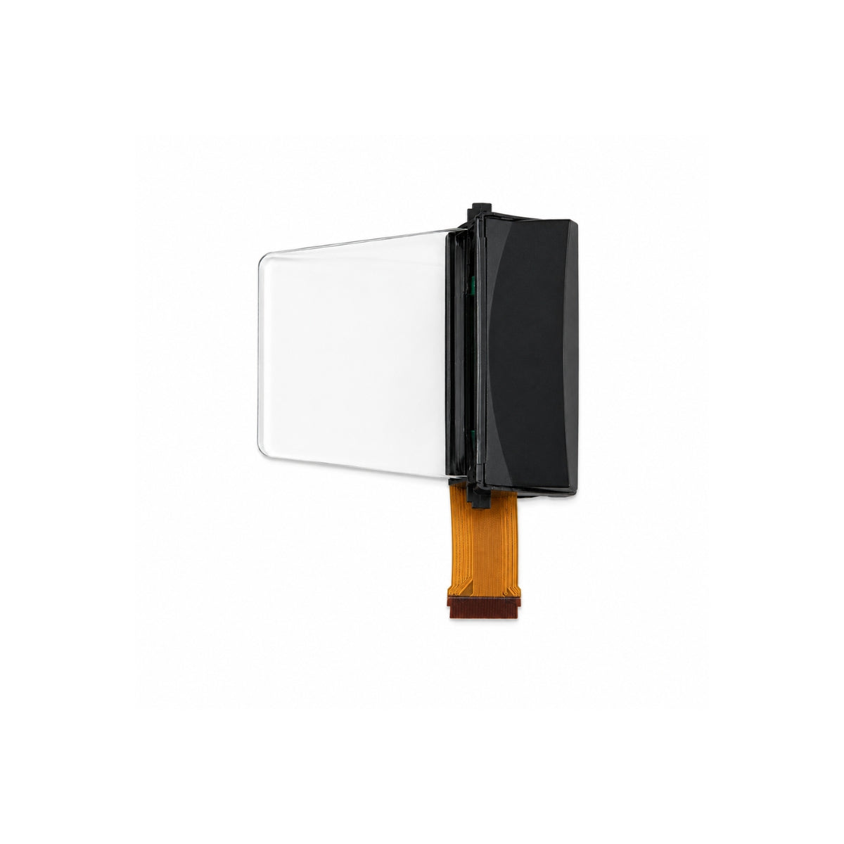
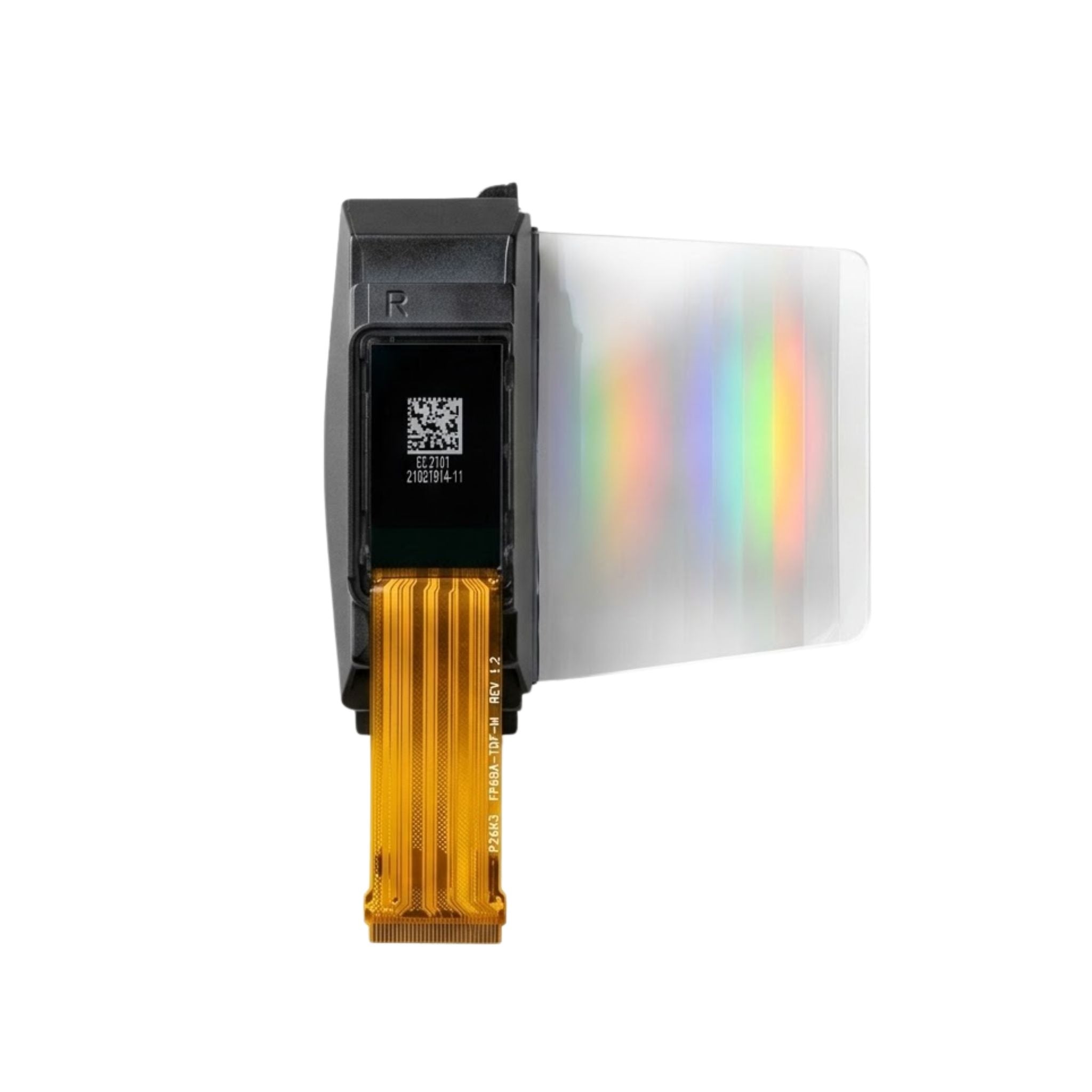


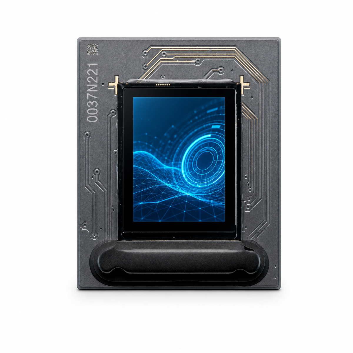
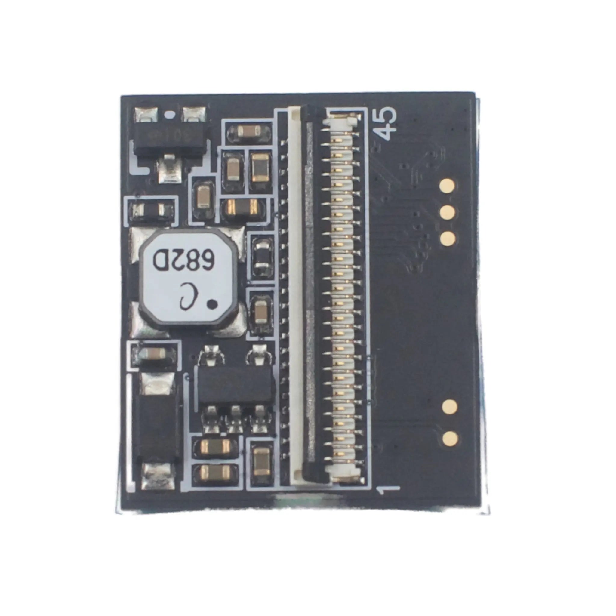
0.39" 1024×768 Micro-OLED | Ultra-Fine Pixel, 1800 cd/m²
- 💹 Enjoy a 20% discount for orders over 500
- 📉 A 15% discount is available for orders ranging from 200 to 499
- 🎁 A 10% discount is available for orders ranging from 50 to 199
- 🎁 A 5% discount is available when ordering 10-49
Interested in customizing this product? Get in touch with us.
Order samples, immediate delivery.
Factory bulk lead time: 3 weeks.
0.39" 1024×768 Micro-OLED | Ultra-Fine Pixel, 1800 cd/m²
- 💹 Enjoy a 20% discount for orders over 500
- 📉 A 15% discount is available for orders ranging from 200 to 499
- 🎁 A 10% discount is available for orders ranging from 50 to 199
- 🎁 A 5% discount is available when ordering 10-49
0.39-Inch 1024×768 Micro-OLED Display with Up to 1,800 cd/m² Luminance
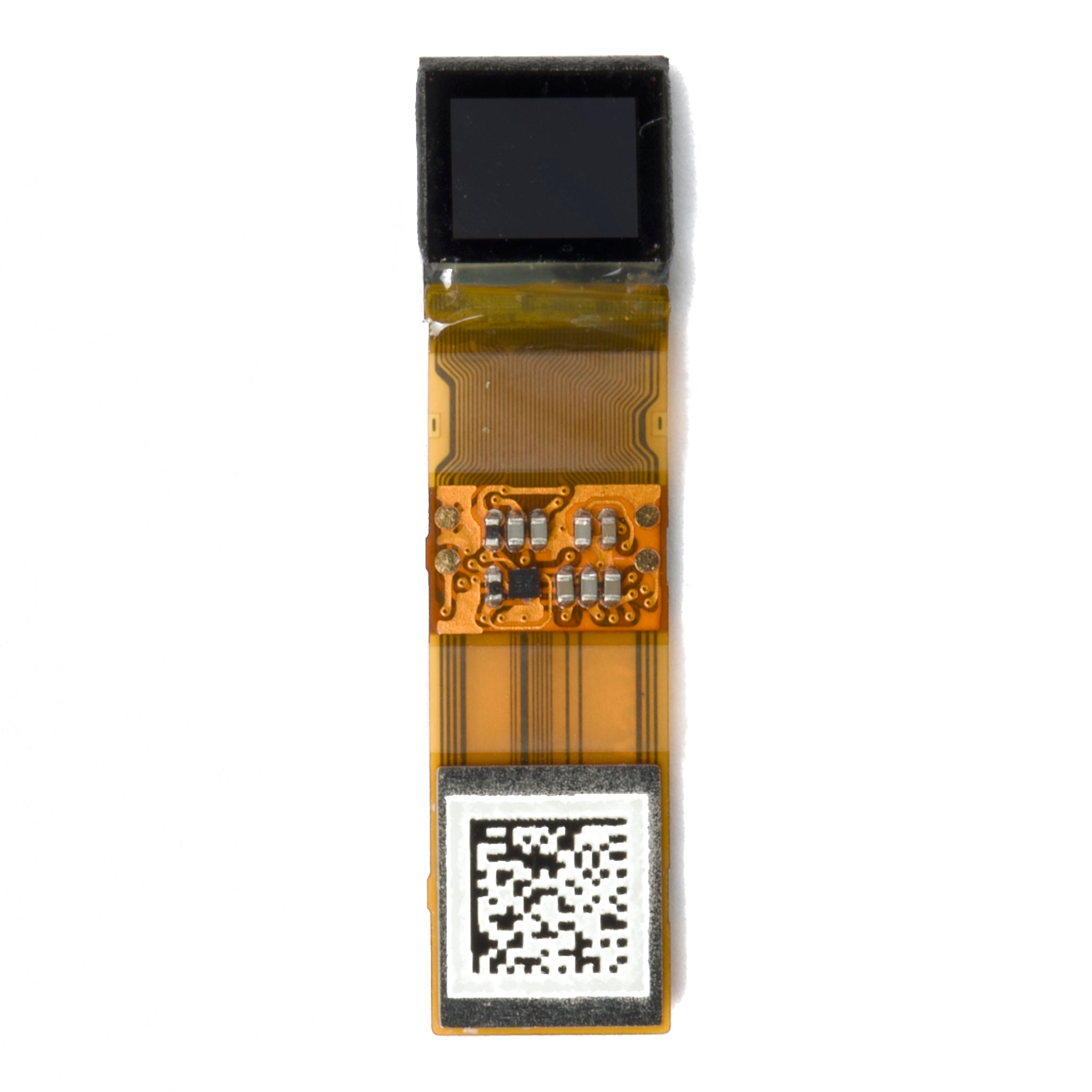
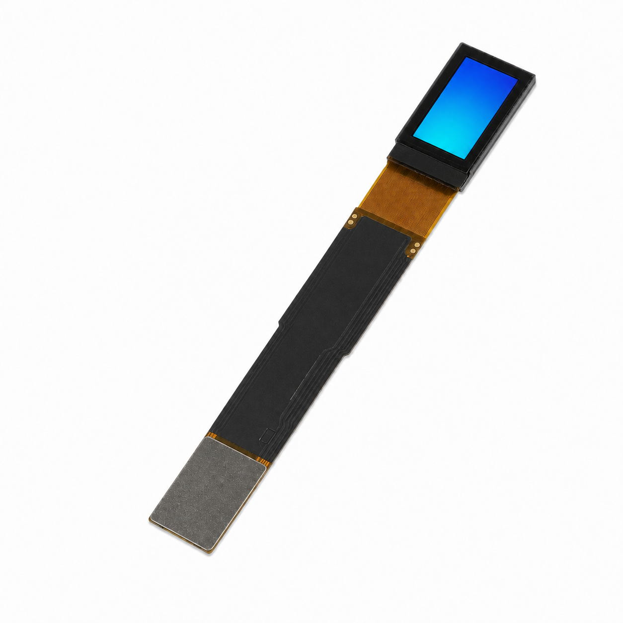
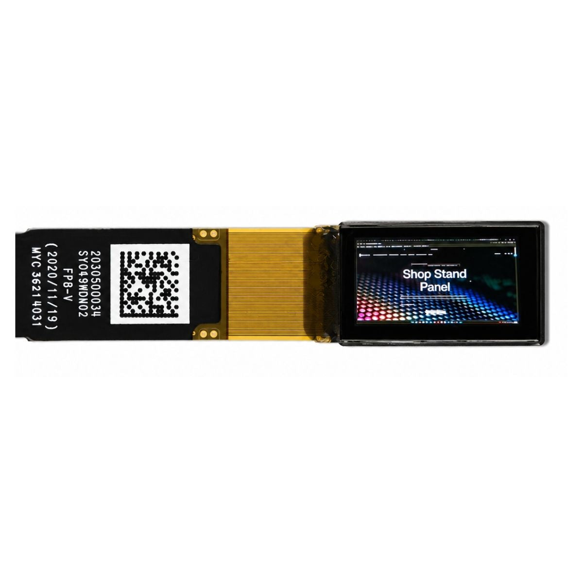
DMGXO0039XGNA is a top-emission, active-matrix silicon-based OLED microdisplay developed for compact near-eye display systems. The module uses a 0.18 µm CMOS silicon backplane and integrates video processing, row and column driving, logic control, I²C register access, brightness adjustment, image positioning, mirroring, and temperature measurement.
The documented video input is a parallel digital interface supporting RGB, YCbCr, and mono data formats. I²C is used separately for register configuration and status access. The detailed pin table identifies a 0.3 mm-pitch, 45-pin flip-lock connector.
Document basis: Product Specification V1.0.0, dated May 13, 2025. The datasheet and controlled mechanical drawing govern final design. Where different datasheet sections list different luminance, contrast, or refresh-rate values, confirm the approved operating condition with DisplayModule before design release.

Datasheet-Based Technical Specifications
The specifications below reproduce values from Product Specification V1.0.0. Values that differ between sections of the same document are shown with their stated context instead of being merged into one unsupported figure.
| Parameter | Documented Specification |
|---|---|
| Product SKU | DMGXO0039XGNA |
| Display Technology | Top-emission, active-matrix silicon-based OLED microdisplay |
| CMOS Process | 0.18 µm CMOS silicon backplane |
| Screen Size | 0.39 inch |
| Resolution | 1024(H)×768(V) pixels |
| Pixel Arrangement | RGB vertical stripe |
| Pixel Size | 0.0078×0.0078 mm, equivalent to 7.8×7.8 µm |
| Active Area | 8.1325(H)×6.1779(V) mm, as listed in the General Specification |
| Grayscale | 256 levels |
| Luminance Uniformity | General Specification: ≥90%. Optical table: 90% minimum, 95% typical, 100% maximum for 5-point uniformity. |
| Published Luminance References | General Specification: 600 cd/m² typical and 1,800 cd/m² maximum. Brightness section: approximately 200 cd/m² factory default. Optical table: 200 cd/m² normal-mode luminance with all pixels on. |
| Recommended Luminance Range | The General Specification lists 40 to 600 cd/m², while the Brightness Adjustment section lists 40 to 400 cd/m². Confirm the approved range for the selected drive configuration before release. |
| Contrast Ratio | General Specification: >10,000:1 typical. Optical table: ≥31,000:1 using highest grayscale to lowest grayscale. Confirm the applicable test condition when setting a procurement requirement. |
| Refresh-Rate References | General Specification: 25 Hz to 75 Hz. The video-timing section additionally provides XGA timing examples at 85 Hz and 120 Hz. Confirm which modes are approved for continuous operation. |
| Video Input Formats | 24-bit RGB 4:4:4; 24-bit YCbCr 4:4:4; 16-bit YCbCr 4:2:2; 8-bit mono |
| Register Interface | I²C, 10 kHz to 400 kHz |
| Connector | 0.3 mm-pitch, 45-pin flip-lock connector |
| Digital Supply | VDD: 1.62 V minimum, 1.80 V typical, 1.98 V maximum |
| OLED Driver Supply | VAN: 4.50 V minimum, 5.00 V typical, 5.50 V maximum |
| VCOM | −4.8 V minimum, −2.0 V typical, −0.2 V maximum |
| Maximum Supply Current | VDD current: 40 mA maximum. VAN current: 25 mA maximum. |
| Digital Input Levels | VIL: −0.3 V to 0.5 V. VIH: 1.2 V to 3.6 V. The datasheet states compatibility with 1.8 V and 3.3 V logic when these limits are met. |
| Typical Power Consumption | 65 mW at 60 Hz and 54 mW at 25 Hz. Test condition: 200 cd/m², +25°C ±2°C, full-white field. |
| White Color Coordinates | x: 0.28 minimum, 0.31 typical, 0.34 maximum. y: 0.30 minimum, 0.33 typical, 0.36 maximum. |
| Operating Temperature | −40°C minimum, +25°C typical, +65°C maximum |
| Storage Temperature | −55°C to +80°C, listed under Absolute Maximum Rating |
| Weight | 1 g |
| Touch Function | No touch-panel specification is provided. Treat this SKU as a non-touch microdisplay unless a separate touch configuration is documented and confirmed. |
Connector, Pin Groups, and Electrical Integration
The detailed pin table documents a parallel digital video bus, synchronization signals, I²C control, grounds, and separate VDD and VAN supply pins. Use the complete official pin table when creating the PCB footprint and schematic.
Interface Clarification
A feature line in the datasheet mentions 3-wire SPI, 4-wire SPI, MCU, and IIC. However, the detailed 45-pin definition documents parallel video data, VS, HS, DE, PCLK, reset, and I²C control pins. Do not design around an SPI or MCU video mode unless DisplayModule supplies model-specific pin and timing documentation for that mode.
During FPC insertion, the datasheet states that the gold fingers should face the carrier board.
Parallel Video Signals
Pins 9 to 33 carry the color or YCbCr data bits. The control group includes VS, DE, reset, HS, and PCLK. Confirm the selected format, bit mapping, sync polarity, and timing before firmware or FPGA release.
I²C Register Access
Pins 1 to 3 provide address selection, SDA, and SCL. The datasheet specifies 10 kHz to 400 kHz communication, pull-up resistors to VIH, and additional signal-integrity care for longer connections.
Power and Ground Pins
Pins 42 and 43 are VAN +5 V supplies for the OLED driver. Pins 44 and 45 are 1.8 V VDD supplies for the digital core. Multiple ground pins are distributed through the connector.
Power Sequence
The datasheet lists a minimum 5 ms power-stabilization time and an EEPROM loading and data-refresh interval of 100 ms minimum, 300 ms typical, and 1,000 ms maximum. Follow the complete sequence diagram for power-on and power-off.
| Digital Timing Item | Documented Value |
|---|---|
| Setup Time | 4 ns minimum |
| Hold Time | 1.5 ns minimum |
| Clock Period | 15.4 ns typical |
| Clock Duty Cycle | 45% minimum, 50% typical, 55% maximum |
Digital Video Formats and XGA Timing References
The default factory video format is 24-bit RGB. The datasheet states that YCbCr operation is not compatible with the default 24-bit RGB configuration and must be redefined for the intended use. Contact DisplayModule technical support before releasing a YCbCr implementation.
| Format | Register Selection and Data Width |
|---|---|
| RGB | 24-bit RGB, 4:4:4 |
| YCbCr | 24-bit YCbCr, 4:4:4 |
| YCbCr | 16-bit YCbCr, 4:2:2 |
| Mono | 8-bit Y[7:0] |
| XGA Timing Example | Pixel Clock and Total Timing |
|---|---|
| 1024×768 at 50 Hz | 54.16 MHz pixel clock; 1334 total pixels per line; 806 total lines |
| 1024×768 at 60 Hz | 65 MHz pixel clock; 1334 total pixels per line; 806 total lines |
| 1024×768 at 70 Hz | 75 MHz pixel clock; 1328 total pixels per line; 806 total lines |
| 1024×768 at 75 Hz | 78.75 MHz pixel clock; 1312 total pixels per line; 800 total lines |
| 1024×768 at 85 Hz | 95.5 MHz pixel clock; 1376 total pixels per line; 808 total lines |
| 1024×768 at 120 Hz | 115.5 MHz pixel clock; 1184 total pixels per line; 813 total lines |
Mode approval: The General Specification lists a 25 Hz to 75 Hz refresh range, while the timing section provides examples at 85 Hz and 120 Hz. Confirm the approved continuous operating modes, luminance limits, and thermal conditions before using the higher-rate examples.
Brightness, Image Control, and Temperature Functions
The datasheet documents register-controlled image functions rather than a fixed-function display path. Use the supplied initialization sequence and register definitions for the exact module revision.
Brightness Adjustment
The document lists PWM-based digital brightness control and DDP data-gain adjustment, with three selectable configuration groups. The factory default brightness is approximately 200 cd/m².
Mirroring and Position
Horizontal and vertical mirroring, timed image shifting, display-position adjustment, and active-area remapping are documented. Validate the final orientation and image window with the intended optical path.
Temperature Measurement
The temperature reading uses registers 00BAH and 00BBH with the documented conversion T = 0.65 × Reg(H) − 375.5. Wait several seconds after power-on before reading; normal updates occur every four frame cycles.
Adaptive Brightness Statement
The feature list states that adaptive brightness adjustment is supported, and the detailed sections document PWM and DDP brightness controls. The document does not identify an integrated ambient-light sensor, so confirm the intended adaptive-control method for the final system.
Internal Test Patterns
Six built-in test patterns are documented: white, black, horizontal grayscale gradient, vertical grayscale gradient, checkerboard, and bright/dark alternating stripes.
Near-Eye System Evaluation
The datasheet positions the module for near-eye display systems requiring compact size, high resolution, low power consumption, and a broad operating-temperature range. Final suitability depends on the complete optical, electrical, thermal, and mechanical design.
Mechanical and Sample Review Before Design Release
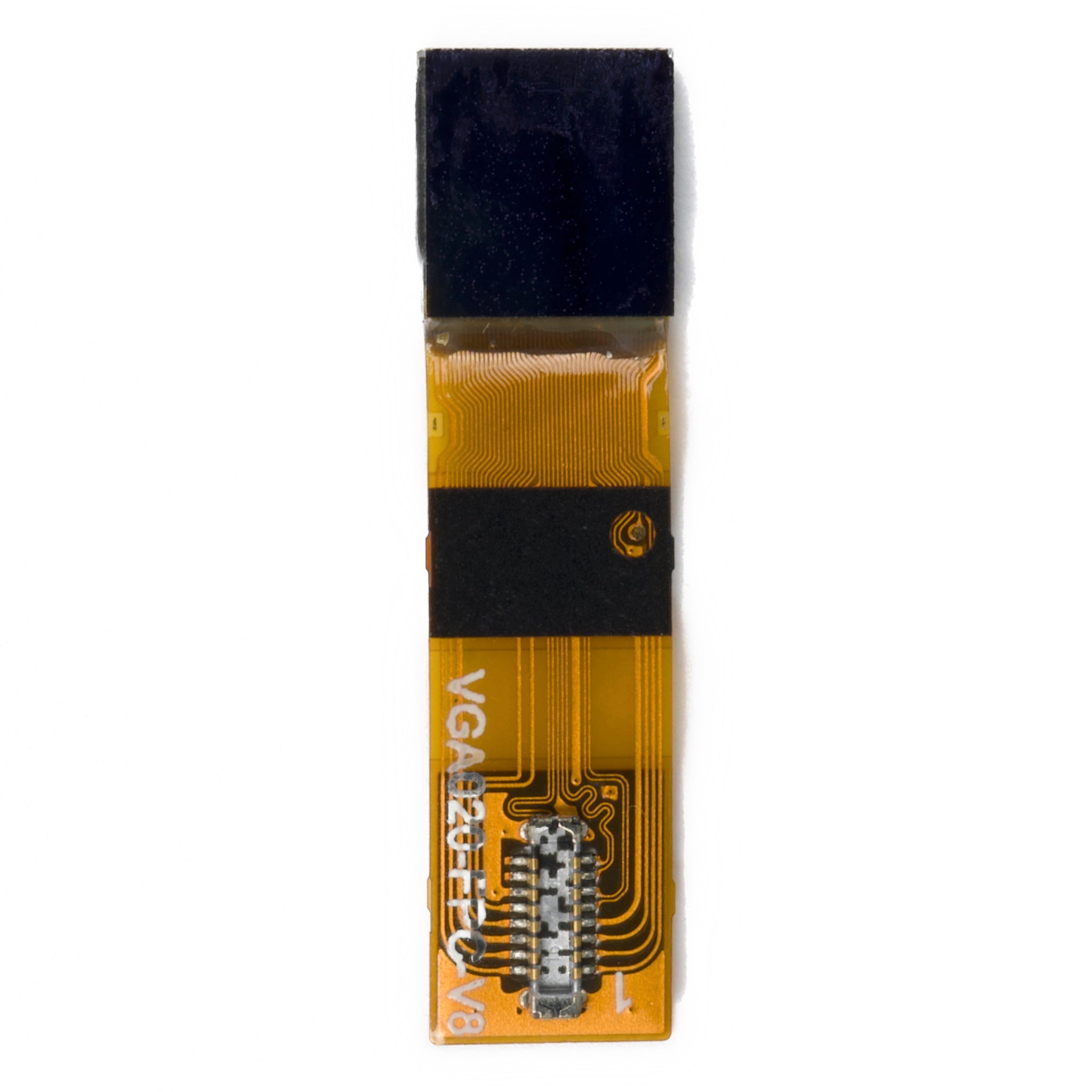
The supplied drawing includes front, side, rear, pixel, connector, and recommended FPC information. Use the controlled drawing and physical samples rather than the nominal screen size alone.
Document Hierarchy
1. Latest official datasheet
2. Controlled mechanical drawing
3. Approved physical sample
4. Product-page summary
Mechanical outline: Review the 16.60±0.10 mm width, 14.20±0.10 mm height, side profile, rear components, and connector clearance shown in the drawing.
Active-area definition: The datasheet separately lists 7.8 µm pixel size and an 8.1325×6.1779 mm active area. Confirm the controlled definition before optical tooling or magnification calculations.
Connector fit: Confirm the 0.3 mm-pitch 45-pin flip-lock connector, mating part, FPC thickness, gold-finger orientation, and insertion clearance.
Power validation: Verify VDD, VAN, VCOM, current capacity, decoupling, sequence timing, reset behavior, and the final thermal condition.
Video validation: Confirm data format, bit mapping, pixel clock, sync polarity, blanking, refresh mode, and the selected YCbCr or RGB configuration.
Procurement: Confirm the datasheet revision, sample status, ordering configuration, lifecycle status, lead time, and annual quantity before volume release.
Common Questions Before Ordering
Is 1,800 cd/m² the normal operating brightness?
No. Product Specification V1.0.0 lists 1,800 cd/m² as maximum. It also lists 600 cd/m² as typical in the General Specification and approximately 200 cd/m² as the factory default and normal-mode optical test point. Confirm the approved brightness and thermal condition for the intended configuration.
What luminance range should be used for design?
The General Specification lists 40 to 600 cd/m², while the Brightness Adjustment section lists 40 to 400 cd/m². Because the same document contains both ranges, obtain written confirmation of the approved operating range before setting the final requirement.
Can SPI transmit the XGA video image?
The feature list mentions SPI and MCU interfaces, but the detailed 45-pin definition documents a parallel video bus plus I²C register control. Do not use SPI as the XGA video path unless DisplayModule provides model-specific interface and timing documentation.
Can I²C transmit the video image?
No. The documented I²C interface is used to read and write internal registers for functions such as initialization, test-pattern selection, brightness, contrast, and temperature access. Live video uses the parallel digital data and timing pins.
Does the module provide adaptive brightness?
The feature list states that adaptive brightness adjustment is supported. The detailed sections document PWM and DDP brightness controls, but do not identify an integrated ambient-light sensor. Confirm the intended adaptive-control method and whether external sensing is required with DisplayModule.
Is a touch panel included?
No touch-panel specification is provided in Product Specification V1.0.0. Treat DMGXO0039XGNA as a non-touch microdisplay unless a separate touch solution is documented and confirmed.
Which storage-temperature value should be used?
The Absolute Maximum Rating table lists −55°C to +80°C for the storage environment. Absolute maximum ratings are not recommended continuous operating conditions, so confirm packaging, handling, and storage requirements for the project.
Which document controls production design?
Use the latest official datasheet and controlled mechanical drawing for the exact SKU. The product page is a selection and evaluation summary and does not replace the complete pin table, timing diagrams, power sequence, register definitions, or approved drawing.
Download Official Datasheet
Review Product Specification V1.0.0 and confirm that the resource page contains the latest revision before schematic capture, PCB layout, FPC release, optical tooling, firmware release, or volume ordering.
Use the official document to verify the complete pin assignment, power sequence, signal timing, I²C register definitions, mechanical drawing, and operating limits.
Product FAQs
Key technical and purchasing guidance for product evaluation, integration planning, samples, and volume orders.