



DM-ADTTR-030 · Micro OLEDoS Display Module
1.03-Inch Micro OLEDoS Display Module, 2560(RGB) × 2560
The DM-ADTTR-030 is a 1.03-inch active-matrix color Micro OLED panel module built on a single-crystal silicon transistor backplane. It provides a native resolution of 2560(RGB) × 2560, approximately 3,515 PPI calculated pixel density, 1800 cd/m² typical luminance at a 30°C panel temperature, and a 500,000:1 typical contrast ratio.
The usable display area is 18.432 mm × 18.432 mm, with a 7.2 µm × 7.2 µm pixel size. The native format contains 6,553,600 full-color pixels and 19,660,800 RGB sub-pixel dots. The integrated panel and logic drivers support compact head-mounted displays, electronic viewfinders and other magnified optical systems.
2560 × 2560
Native RGB resolution
Approx. 3,515 PPI
Calculated pixel density
1800 cd/m²
Typical panel luminance
500,000:1
Typical contrast ratio
7.2 µm
Pixel size
18.432 mm
Square active-area width
Optical, Mechanical and Electrical Specifications
| Parameter | Specification | Engineering Note |
|---|---|---|
| Display Technology | Active-matrix color Micro OLED / OLEDoS | Single-crystal silicon transistor backplane |
| Model Basis | SY103WAM01 | Confirm the supplier model and datasheet revision on the approved purchase specification |
| Nominal Diagonal | 1.03 inches | Square 1:1 active image format |
| Native Resolution | 2560(H) × 2560(V) RGB | 6,553,600 full-color pixels |
| Number of Dots | 19.66M RGB sub-pixel dots | 2560 × 2560 × 3 = 19,660,800 dots |
| Calculated Pixel Density | Approximately 3,515 PPI | Calculated from the native resolution and nominal 1.03-inch diagonal |
| Pixel Size | 7.2 µm × 7.2 µm | Use the official drawing for optical simulation and tolerance analysis |
| Pixel Arrangement | RGB π type | Real RGB pixel structure |
| Usable Display Area | 18.432 mm × 18.432 mm | Confirm optical center and mechanical position from the controlled module drawing |
| Brightness at 30°C | 1800 cd/m² typical | Measured at full-white gray level 255 in a dark-room optical setup |
| Brightness from 10°C to 70°C | 1350 min. / 1800 typ. / 2250 max. cd/m² | Display-side values; completed-system brightness depends on optical transmission |
| Contrast Ratio | 200,000:1 minimum / 500,000:1 typical | White-to-black contrast under the datasheet measurement conditions |
| Luminance Uniformity | 85% minimum | Defined as minimum luminance divided by maximum luminance across nine measurement areas |
| Color Gamut | DCI-P3: 80% minimum / 90% typical | Final color at the eye may change after lenses, coatings and optical combiners |
| Gray Levels | 256 | Normal operation supports 16.7 million colors |
| White Viewing Angle | 35° minimum | Defined at the point where white luminance falls to 50% |
| Video Interface | MIPI D-PHY, one or two ports | Four lanes with one port or eight lanes with two ports |
| MIPI Data Rate | Up to 1.0 Gbps per lane | MIPI D-PHY v1.2 and MIPI DSI v1.01 R11 video mode |
| Control Interface | I2C | Used for command and register control |
| Compression Support | VESA DSC v1.1 in-chip decoder | Supports a documented 3:1 compression ratio |
| Native-Input Frame Rate | 60 Hz to 75 Hz | Maximum 75 Hz for 2560 × 2560 input with DSC enabled |
| Scaled-Input Frame Rate | Up to 90 Hz | Applies to 1920 × 1920 input scaled 1.33× to 2560 × 2560 with DSC enabled |
| Scaling Support | 1.33× and 2× | Supports 1920 × 1920 and 1280 × 1280 source formats scaled to the native panel resolution |
| Operating Voltage | VDDI 1.8 V; AVDD 5.8-6.0 V; AVEE -4.0 to -5.5 V | Follow the complete power-generation and power-sequence sections before schematic release |
| Power Consumption | 1600 mW typical / 2000 mW maximum | At 1800 nits, 100% duty, 1920 × 1920 input, 1.33× scaling, no DSC and 72 Hz |
| Operating Temperature | -20°C to +70°C | Validate image performance and thermal conditions in the completed enclosure |
| Storage Temperature | -40°C to +80°C | Observe the handling, moisture, static-control and storage precautions in the datasheet |
| Module Weight | Approximately 2 g | Connector, support board and optical components are not included in this value |
Measurement basis: Unless otherwise specified, optical values are defined at 30°C. Brightness is measured at the center of the screen using a full-white pattern at gray level 255 in a dark room.
Pixel Architecture and Image Performance
Real RGB Pixel Structure
The native 2560 × 2560 image contains 6.55 million full-color pixels and 19.66 million RGB sub-pixel dots. Real RGB rendering avoids treating the quoted dot count as the number of independent full-color pixels.
Optical Brightness Budget
The 1800 cd/m² typical value is measured at the panel. Eye-side luminance is reduced by lenses, prisms, coatings, polarizers, combiners or waveguides in the completed optical path.
Contrast and Black Level
The datasheet specifies a minimum contrast ratio of 200,000:1 and a typical value of 500,000:1. Stray light, reflections and optical leakage may reduce system-level contrast.
Color and Uniformity
DCI-P3 coverage is listed at 80% minimum and 90% typical, while large-area luminance uniformity is at least 85%. Gamma, white point and optical color shift require system-level calibration.
Interface, Driver and System Integration
MIPI D-PHY Configuration
The panel supports one-port or two-port MIPI D-PHY operation. One-port operation provides four data lanes, while two-port operation provides eight data lanes. The documented maximum data rate is 1.0 Gbps per lane.
Integrated Driver Architecture
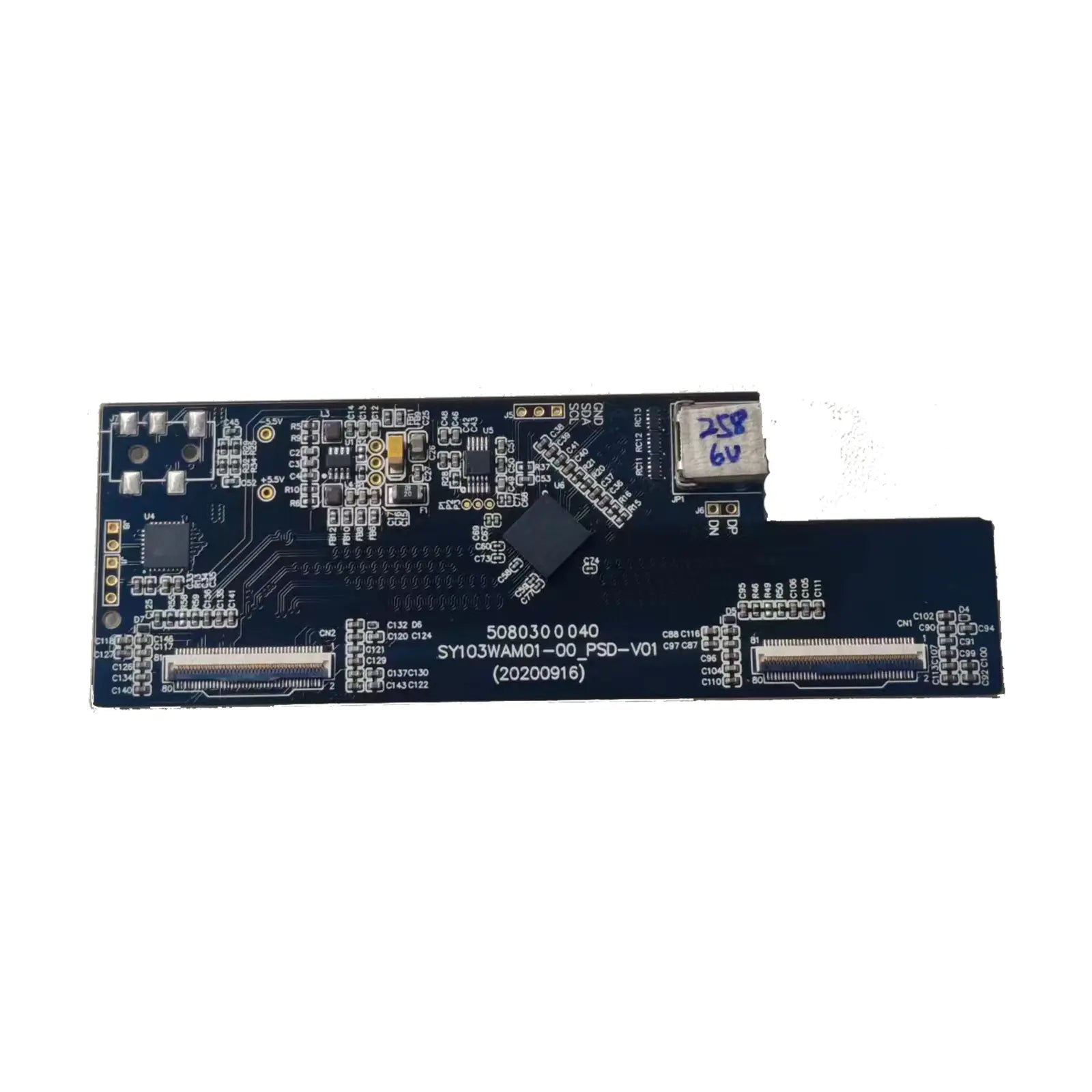
The panel and logic drivers are integrated into the silicon-based display architecture. The host design must still provide the required MIPI video input, I2C control, power rails and initialization sequence.
DSI Video Mode and DSC
The display supports MIPI DSI video mode and an in-chip VESA DSC v1.1 decoder with a documented 3:1 compression ratio. DSC settings must match the host processor and selected input resolution.
Frame Rate Depends on Input Mode
A general value of 60-90 Hz does not describe every resolution mode. Native 2560 × 2560 input with DSC supports up to 75 Hz, while 1920 × 1920 input scaled 1.33× to the native resolution supports up to 90 Hz with DSC.
Mechanical Dimension Reference

18.432 mm
Active width
18.432 mm
Active height
7.2 µm
Pixel size
Approx. 2 g
Module weight
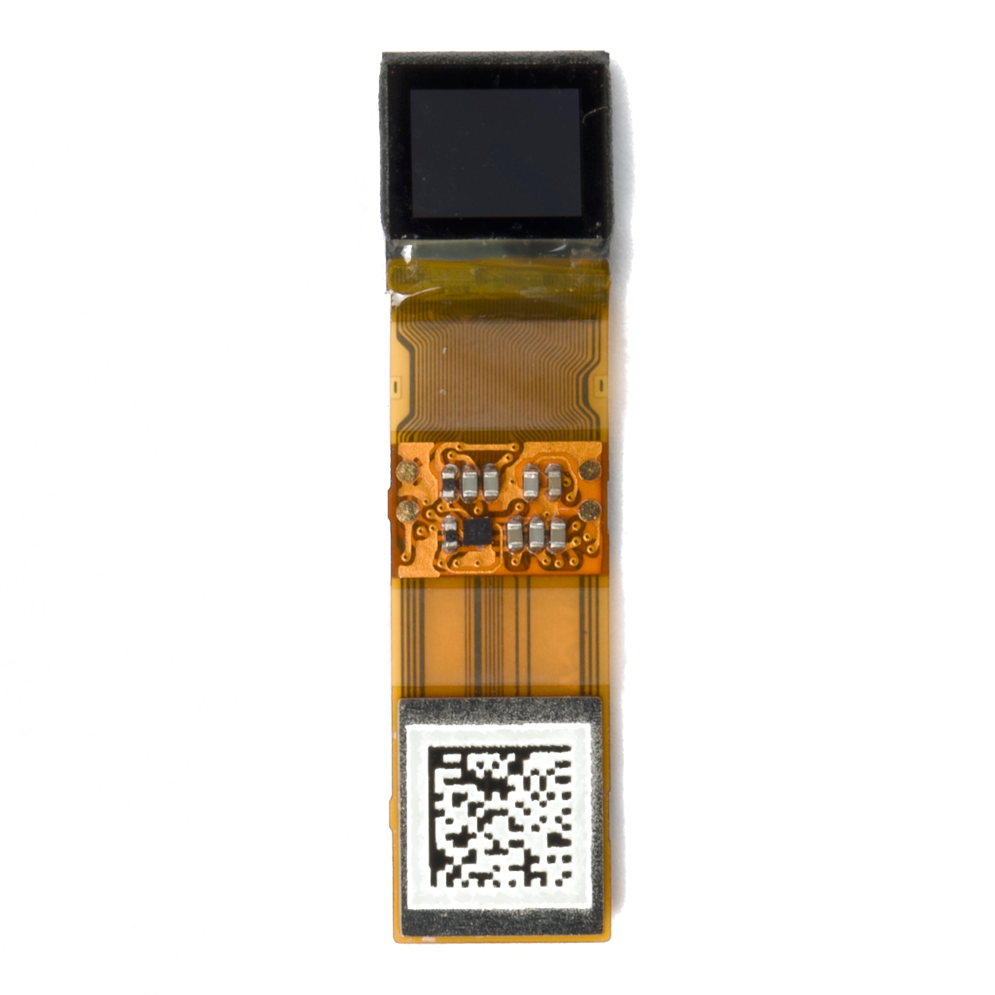
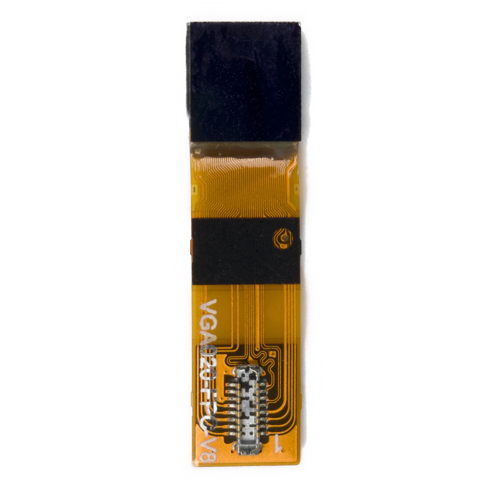
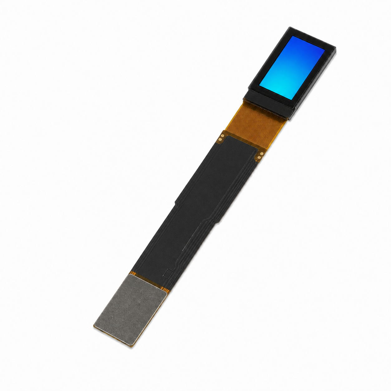
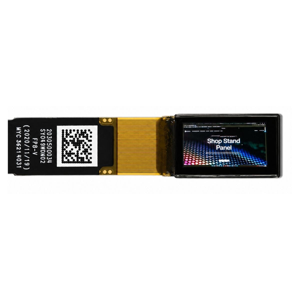
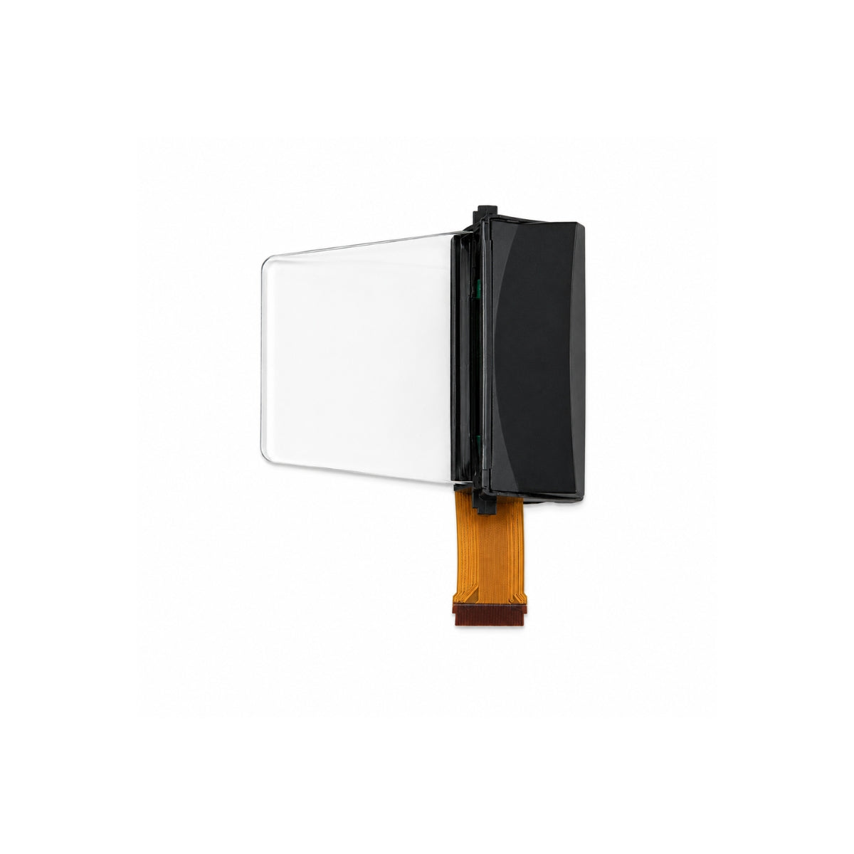
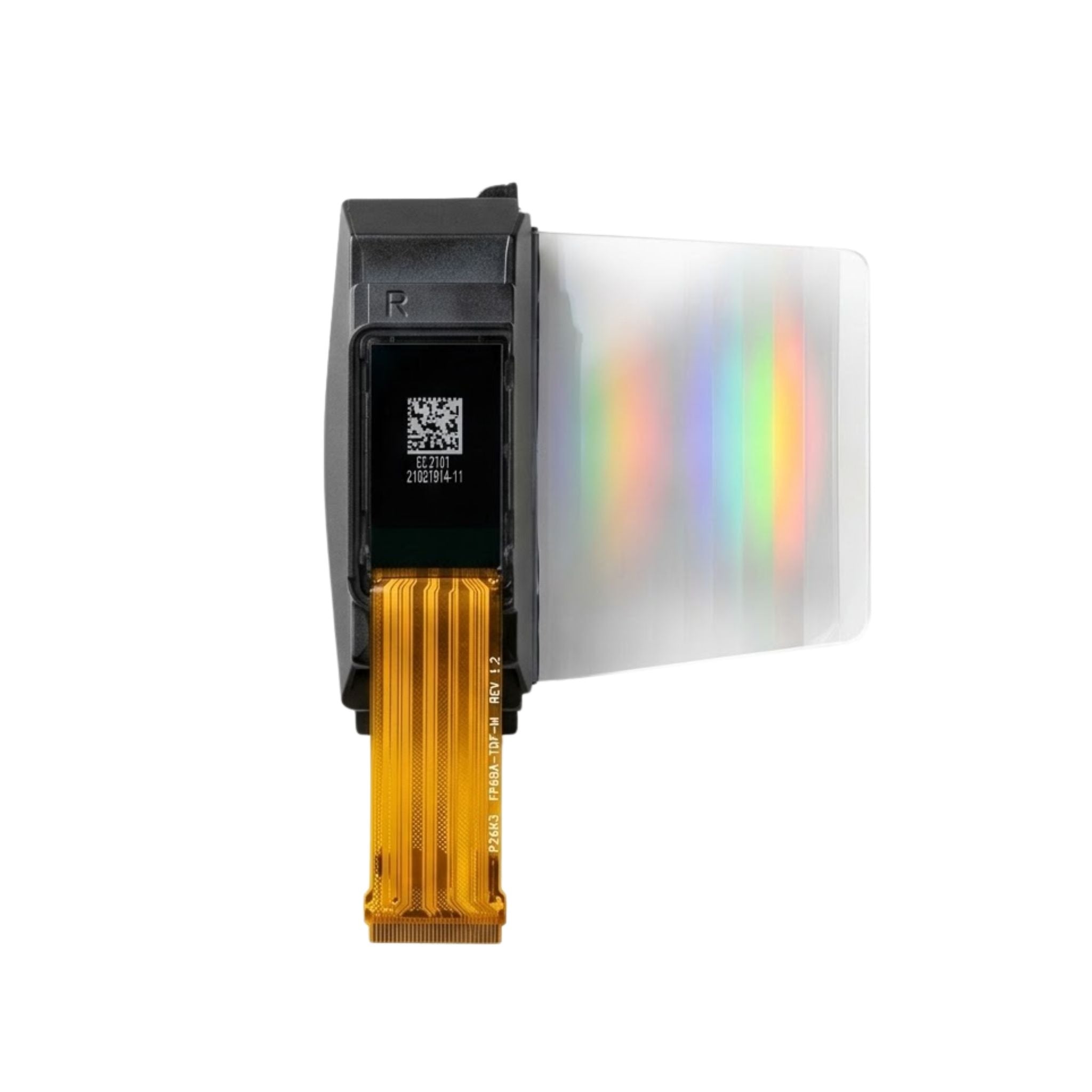
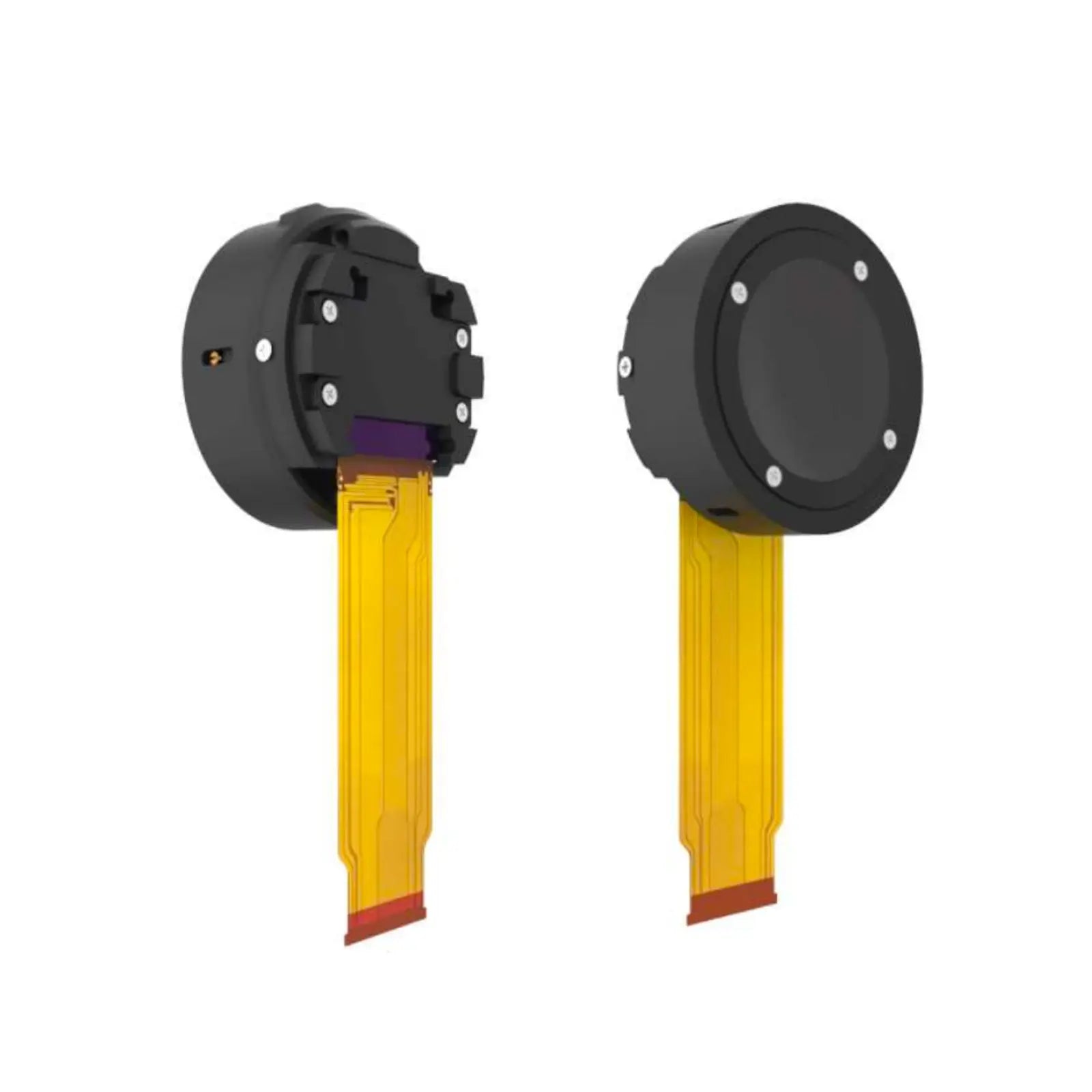
Use the controlled mechanical drawing to verify the active area position, optical center, panel outline, cover-glass dimensions, FPC direction, connector position, bending region and mounting keep-out area.
The displayed image is suitable for preliminary evaluation only. Do not derive production tooling dimensions from the web image or the nominal active-area dimensions.
Application Fit and Verification Points
Head-Mounted Displays
The square native format, real RGB pixels and calculated density above 3,500 PPI support evaluation in magnified head-mounted optics. Verify field of view, eye relief, eye box, lens MTF and optical distortion.
Electronic Viewfinders
High pixel density and OLED black levels suit compact viewfinder evaluation. Confirm input scaling, frame rate, color tuning, optical magnification and enclosure temperature during continuous operation.
See-Through AR Evaluation
Panel luminance alone cannot establish suitability for see-through AR. Measure brightness after the complete optical path and test the system against its intended ambient-light and contrast requirements.
Professional Optical Equipment
The module may be evaluated for medical viewers, inspection systems and imaging instruments. Regulatory approval, safety, cleaning resistance and device reliability must be assessed at the finished-product level.
Selection Notes for OEM Engineering Teams
Match the Optical Engine
Use the 18.432 mm square active area and 7.2 µm pixel size to calculate magnification, field of view, angular resolution, eye box and alignment tolerance.
Plan MIPI Bandwidth
Select the lane count, port count, input resolution, DSC mode and target frame rate before freezing the processor, connector and PCB architecture.
Design the Thermal Path
The optical test condition lists 1600 mW typical and 2000 mW maximum power consumption. Measure actual thermal rise under the selected brightness, duty cycle and frame rate.
Validate Image Stability
Test gamma, white point, luminance uniformity, temperature compensation, image retention, orbit operation and long-duration high-brightness performance.
Documentation and Procurement Checks
Controlled Technical Data
Confirm the model number, datasheet version, electrical tables, module drawing, pin assignment, power sequence, MIPI timing and approved initialization settings.
Prototype Verification
Check image timing, DSC compatibility, optical alignment, brightness control, panel temperature, power sequencing, reset behavior and repeated sleep-wake operation.
Volume Procurement
Confirm sample status, MOQ, lead time, packaging, ESD controls, lot traceability, inspection criteria, warranty, product-change notification and lifecycle supply status.
Technical Resources
Datasheet Review
Review absolute maximum ratings, DC characteristics, MIPI timing, reset timing, power sequencing, commands, reliability tests and handling precautions.
Interface Review
Confirm D-PHY port selection, data-lane configuration, DSI video mode, DSC settings, I2C control, reset timing, impedance and signal-integrity requirements.
Integration Review
Check the mechanical stack, FPC routing, connector, power rails, thermal path, optical axis, production test method and transition from sample to volume production.
DM-ADTTR-030 Official Datasheet
Download and review the technical document before schematic design, optical simulation, firmware integration or prototype validation.