



1.2" Round AMOLED Display 390x390 Full Color - MIPI, SPI
- 💹 Enjoy a 20% discount for orders over 500
- 📉 A 15% discount is available for orders ranging from 200 to 499
- 🎁 A 10% discount is available for orders ranging from 50 to 199
- 🎁 A 5% discount is available when ordering 10-49
Interested in customizing this product? Get in touch with us.
Order samples, immediate delivery.
Factory bulk lead time: 3 weeks.
1.2" Round AMOLED Display 390x390 Full Color - MIPI, SPI
- 💹 Enjoy a 20% discount for orders over 500
- 📉 A 15% discount is available for orders ranging from 200 to 499
- 🎁 A 10% discount is available for orders ranging from 50 to 199
- 🎁 A 5% discount is available when ordering 10-49
Resources & Downloads
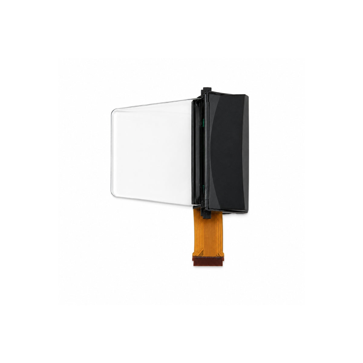
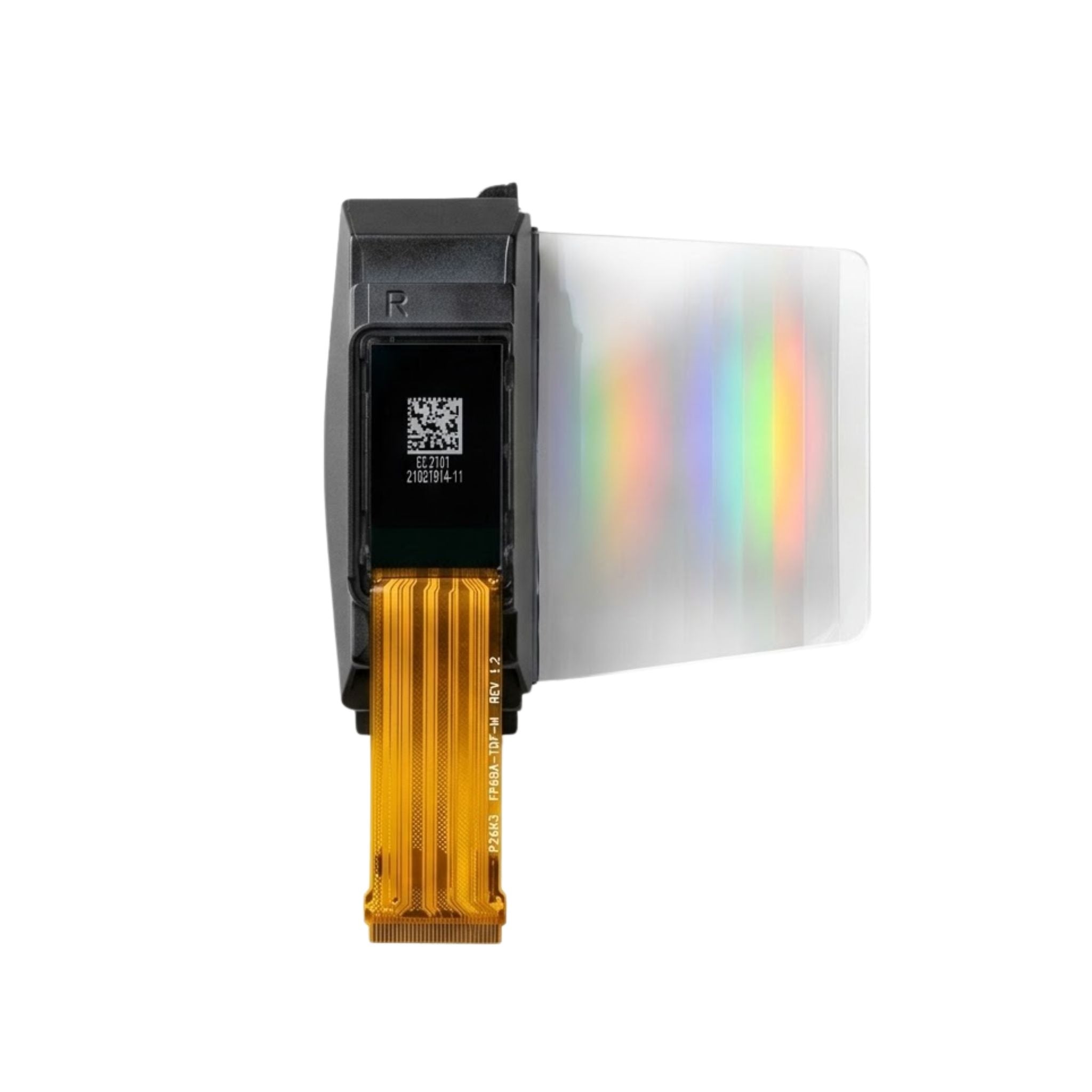
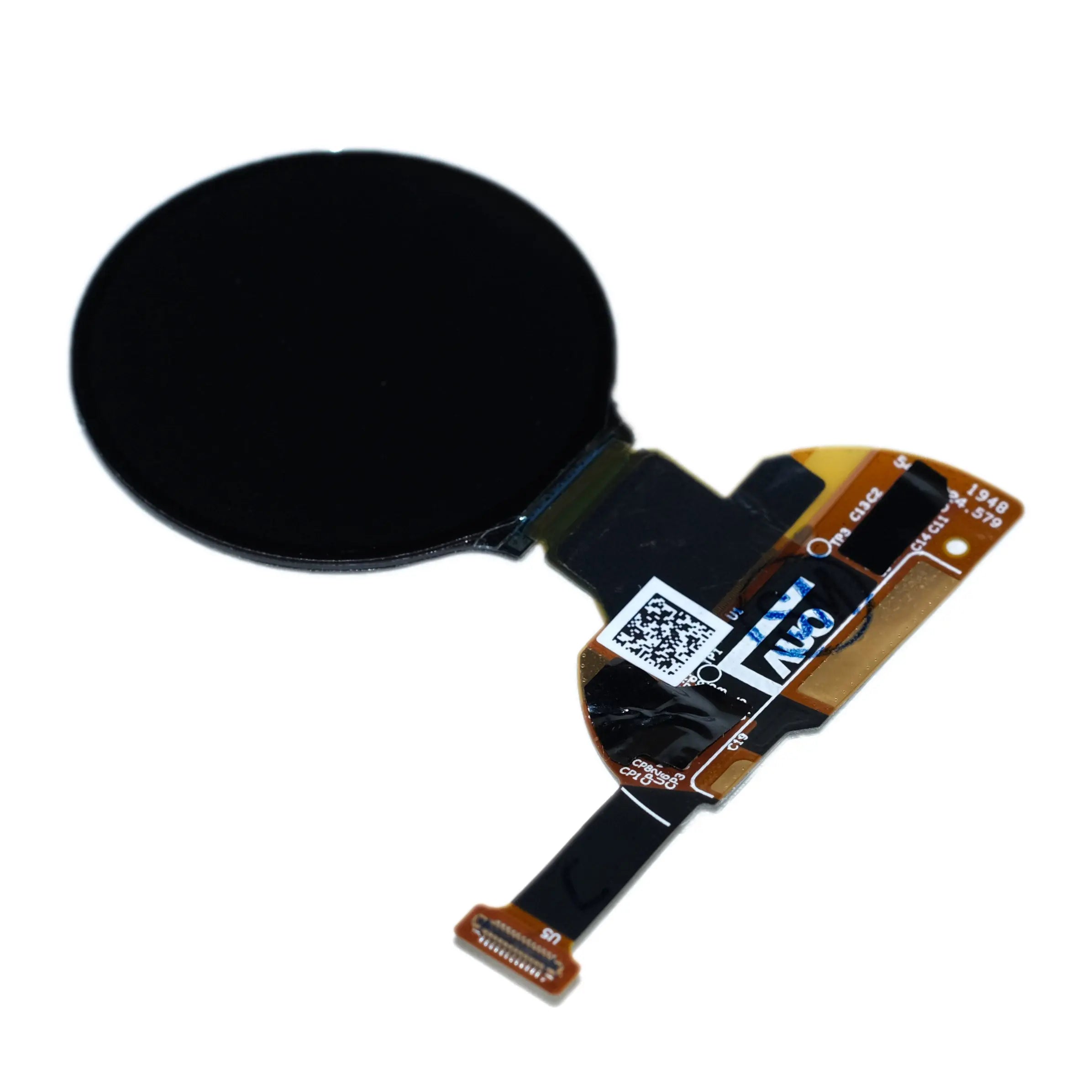
1.2-Inch Round AMOLED Display, 390×390, MIPI Command Mode and SPI
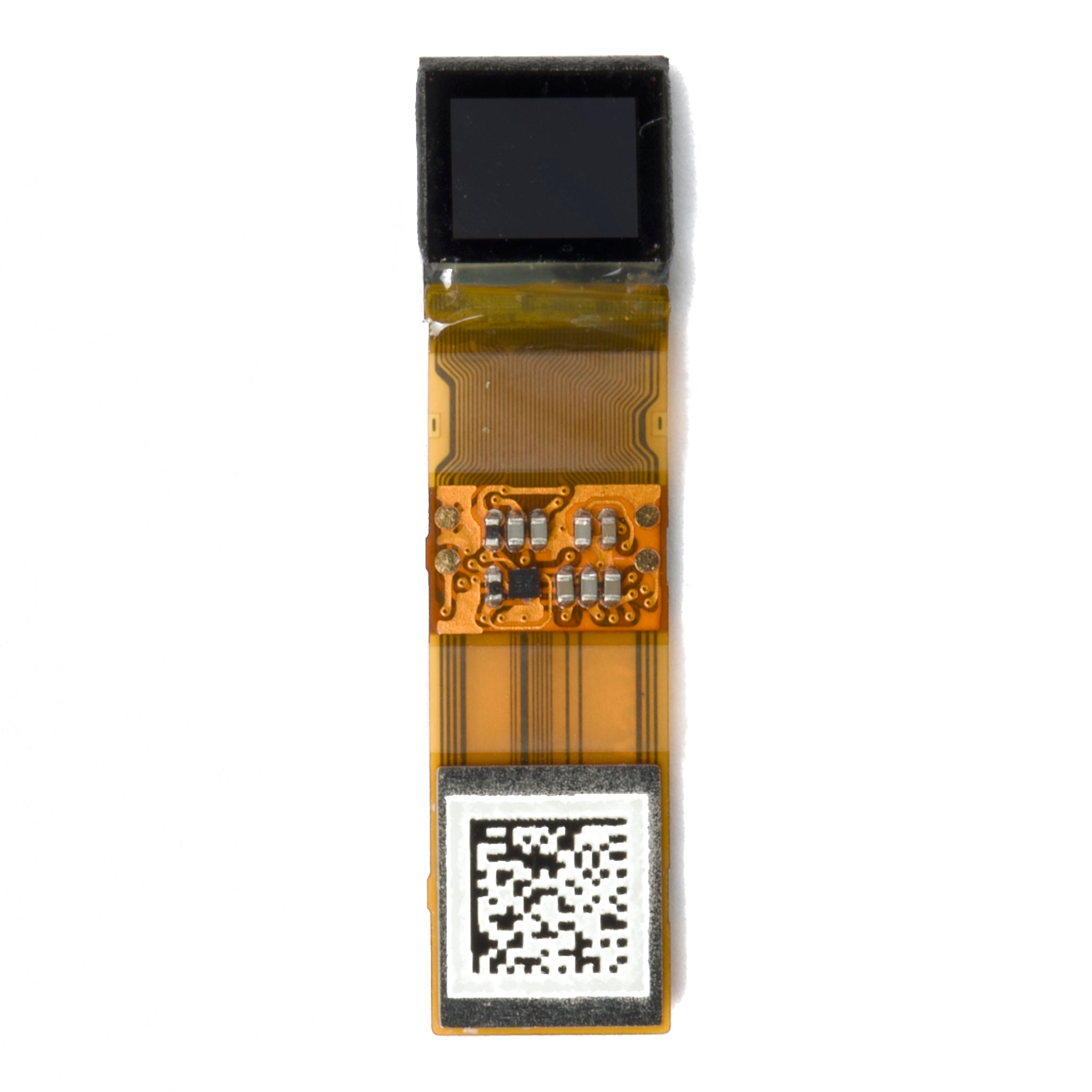
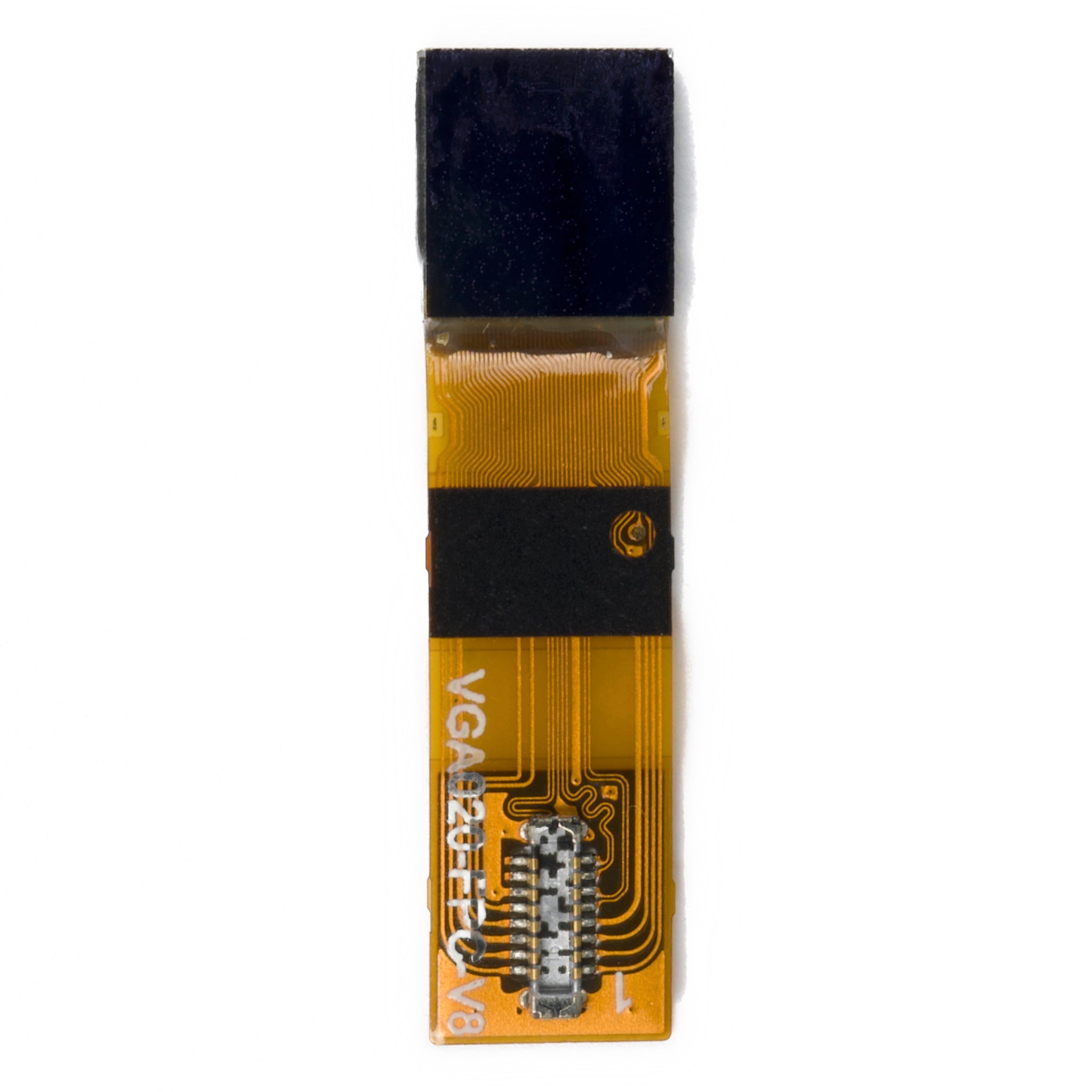
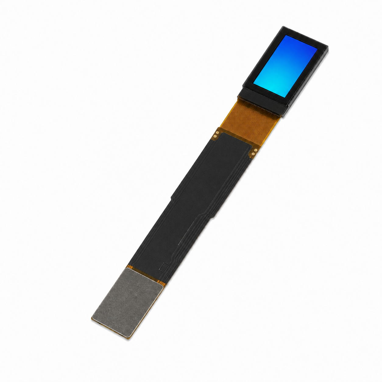
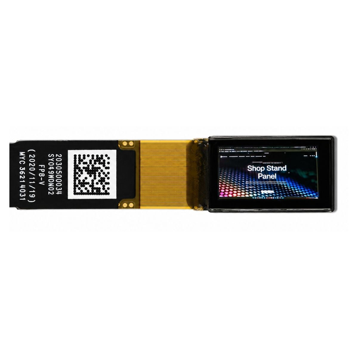
DM-OLED12-667 is a 1.20-inch circular AMOLED display with a 390×390 pixel matrix, a 30.42×30.42 mm active area, Hyper R.G.B pixel configuration, and 16.7 million colors. The module uses MIPI command mode and SPI interfaces through a 24-pin FPC connection.
The published optical specification includes 350 nits typical center brightness, 300 nits minimum brightness, and a 10,000:1 minimum contrast ratio under the stated measurement conditions.
Technical reference: The specifications below are based on the X120BLN02 Product Specification, Version 1.2, dated March 7, 2017. Final mechanical and electrical design should follow the latest approved module datasheet revision.

Mechanical drawing showing the circular panel, active area, FPC assembly, component clearance, thickness, and connector orientation.
Verified Technical Specifications
The following values are taken from the X120BLN02 module specification and mechanical drawing.
| Parameter | Verified Specification |
|---|---|
| Product Type | Round full-color AMOLED display panel |
| DisplayModule SKU | DM-OLED12-667 |
| Panel Model | X120BLN02 |
| Document Revision | Version 1.2, March 7, 2017 |
| Display Size | 1.20 inch |
| Resolution | 390×390 pixels |
| Display Coordinates | Start point: 0, 0. End point: 389, 389. |
| Color Configuration | Hyper R.G.B |
| Color Depth | 16.7 million colors |
| Display Mode | AMOLED |
| Outline Dimension | 33.22 (H)×34.72 (V)×0.66 (T) mm |
| Active Area | 30.42 (H)×30.42 (V) mm |
| Interface | MIPI command mode and SPI |
| Display IC | AUO W022 ASIC |
| FPC Connection | 24-pin AMOLED panel input/output signal interface |
| Recommended FPC-Side Connector | BM28B0.6-24DP/2-0.35V(51) |
| Recommended Main-Board Connector | BM28B0.6-24DS/2-0.35V(51) |
| Normal Brightness | 300 nits minimum; 350 nits typical |
| Boost-Mode Brightness | 500 nits typical; only brightness is guaranteed in boost mode |
| Contrast Ratio | 10,000:1 minimum at 25°C |
| Brightness Uniformity | 85% minimum at 350 nits |
| Viewing Angle | 80° minimum in the top, bottom, left, and right directions |
| NTSC | 87% minimum; 100% typical |
| Gamma | 2.0 to 2.4; 2.2 typical |
Optical Performance
Brightness is measured at the center of the display with a full-white image. The published test condition uses a 25°C±2°C ambient temperature and a dark-room environment.
Viewing-angle values are specified at a contrast-ratio condition above 1600. Cover-window material, optical bonding, enclosure geometry, and viewing direction affect the final visual result.
Additional Optical Values
The module specification lists a 7500 K color temperature and 500 nits typical brightness in boost mode. The boost-mode note states that only brightness is guaranteed while this mode is active.
LT95 Burn-In Metric
The published LT95 value is 150 hours minimum at 25°C with a white-background pattern at 100% loading. LT95 is defined as the time required for luminance to decrease to 95% of its initial value under this test condition.
Electrical Rails and Published Power Data
The module uses separate digital, analog, positive OLED, and negative OLED rails. The host power design must follow the specified voltage ranges and power sequence.
Recommended Operating Rails
The power-structure drawing also uses VCI at 3.3 V typical. PCB design should follow the rail naming, bypass-capacitor arrangement, enable control, and sequence shown in the module specification.
Full-White Panel Power
The panel power table lists 128.7 mW maximum and 19.5 mA maximum with ELVDD at 3.3 V and ELVSS at -3.3 V, based on an L255 full-white pattern at 350 nits.
Normal Mode
The IC power table lists 5.3 mW typical and 1.6 mA typical on the 3.3 V VCI test rail, plus 3.5 mW typical and 1.9 mA typical on VDDIO at 1.8 V, using a black pattern in command mode.
Idle Mode
The power table lists 4.5 mW typical and 1.4 mA typical on the VCI test rail, plus 2.4 mW typical and 1.3 mA typical on VDDIO, using a black pattern through MIPI command mode or SPI.
Sleep Mode
The table lists below 0.075 mW and below 22.6 µA on the VCI test rail, and below 0.1 mW and below 55 µA on VDDIO.
Mechanical Integration Details
The mechanical drawing defines the circular panel, active area, FPC route, foam tape, component area, pull tab, connector location, and thickness stack.
Enclosure window: The visible opening should follow the active area and the optical margin required by the final product design.
FPC clearance: The FPC component area, connector, pull tab, and bend path require clearance from enclosure pressure and sharp edges.
Assembly protection: Avoid concentrated pressure on the glass, FPC bond, connector, and component area during installation.
Connector and Interface Details
The FPC exposes one MIPI data pair, one MIPI clock pair, SPI input and output signals, reset, tearing-effect output, power-control enable, grounds, VDDI, and VBAT connections.
Recommended Connector Pair
The module datasheet identifies the following board-to-board connector pair.
BM28B0.6-24DP/2-0.35V(51)
BM28B0.6-24DS/2-0.35V(51)
MIPI Signals
Pin 6 DSI_D0N, Pin 8 DSI_D0P, Pin 12 DSI_CLKN, and Pin 14 DSI_CLKP. The module uses MIPI command mode.
SPI Signals
Pin 7 CSX, Pin 9 SCL, Pin 11 DCX, Pin 13 SDI, and Pin 15 SDO. The datasheet includes separate SPI write and read timing.
Power and Ground
Ground is assigned to Pins 4, 10, and 16. VDDI is assigned to Pins 18 and 20. VBAT is assigned to Pins 19 and 21 through 24. Pin 2 is VCI_EN.
Control and Reserved Pins
Pin 1 XRES is the active-low reset input. Pin 5 TE is the vertical-sync output. Pins 3 and 17 are marked NC and remain floating.
Reset and Power-Sequence Requirements
The host hardware and firmware must follow the module-level power-on sequence, power-off sequence, and reset timing.
Published Reliability Test Conditions
These values describe the environmental and electrical test conditions listed in the X120BLN02 product specification.
Datasheet Judgment Criterion
The reliability table uses no functional defect after the specified exposure as its judgment criterion.
High-Temperature Operation
70°C for 240 hours
High-Temperature Storage
80°C for 240 hours
Low-Temperature Operation
-20°C for 240 hours
Low-Temperature Storage
-30°C for 240 hours
Humidity Operation
60°C at 90% RH for 120 hours
Humidity Storage
60°C at 90% RH for 240 hours
Thermal Shock
-30°C to 70°C, 30-minute dwell at each condition, 100 cycles, non-operating
Contact ESD
±4 kV contact-discharge test, 150 pF / 330 Ω, power on, five specified test positions
Air ESD
±8 kV air-discharge test, 150 pF / 330 Ω, power on, five specified test positions
Engineering Integration Notes
The module requires coordinated electrical, mechanical, optical, and firmware design.
Power design: Use the specified VDDIO, VBAT, ELVDD, ELVSS, VCI_EN control, bypass capacitors, and power sequence.
Connector design: Match the connector footprint, contact direction, mating height, FPC orientation, and mechanical keep-out area.
MIPI design: Follow the single data lane, clock pair, command-mode timing, reset sequence, and TE signal behavior.
SPI design: Use the published CSX, SCL, DCX, SDI, and SDO pin assignments and the specified read and write timing.
Optical design: Evaluate brightness, uniformity, viewing angle, window transmission, bonding material, and enclosure geometry together.
Mechanical design: Protect the glass, FPC bond, component area, connector, and pull tab from concentrated assembly pressure.
AMOLED Image-Retention Precautions
The module precautions state that displaying a fixed pattern for an extended period can cause image sticking.
Screen timeout, content movement, brightness control, reduced static-image duration, and suitable idle-screen behavior help limit prolonged exposure to fixed high-brightness graphics.
Common Questions
Does the module operate from one 1.8 V supply?
No. VDDIO is 1.8 V typical, while the module also uses 3.3 V typical VBAT and ELVDD rails and a -3.3 V typical ELVSS rail.
What is the active display area?
The active area is 30.42×30.42 mm within the published 33.22×34.72 mm module outline envelope.
Which display IC is specified?
The X120BLN02 module specification identifies the display IC as AUO W022 ASIC.
What brightness is specified?
The normal optical specification is 300 nits minimum and 350 nits typical. Boost mode is listed at 500 nits typical, with brightness as the only guaranteed boost-mode value.
Which interfaces are available?
The module provides MIPI command mode and SPI through its 24-pin FPC connection.
How should static images be managed?
Use screen timeout, image movement, brightness control, and reduced static-image duration to limit prolonged exposure to fixed high-brightness graphics.
Download Technical Resources
Use the official module datasheet as the primary reference for dimensions, pin assignments, electrical rails, optical performance, interface timing, power sequence, and reliability test conditions.
The RM67162 reference datasheet, example code, and STEP model are retained as additional technical resources for firmware review and mechanical integration.