



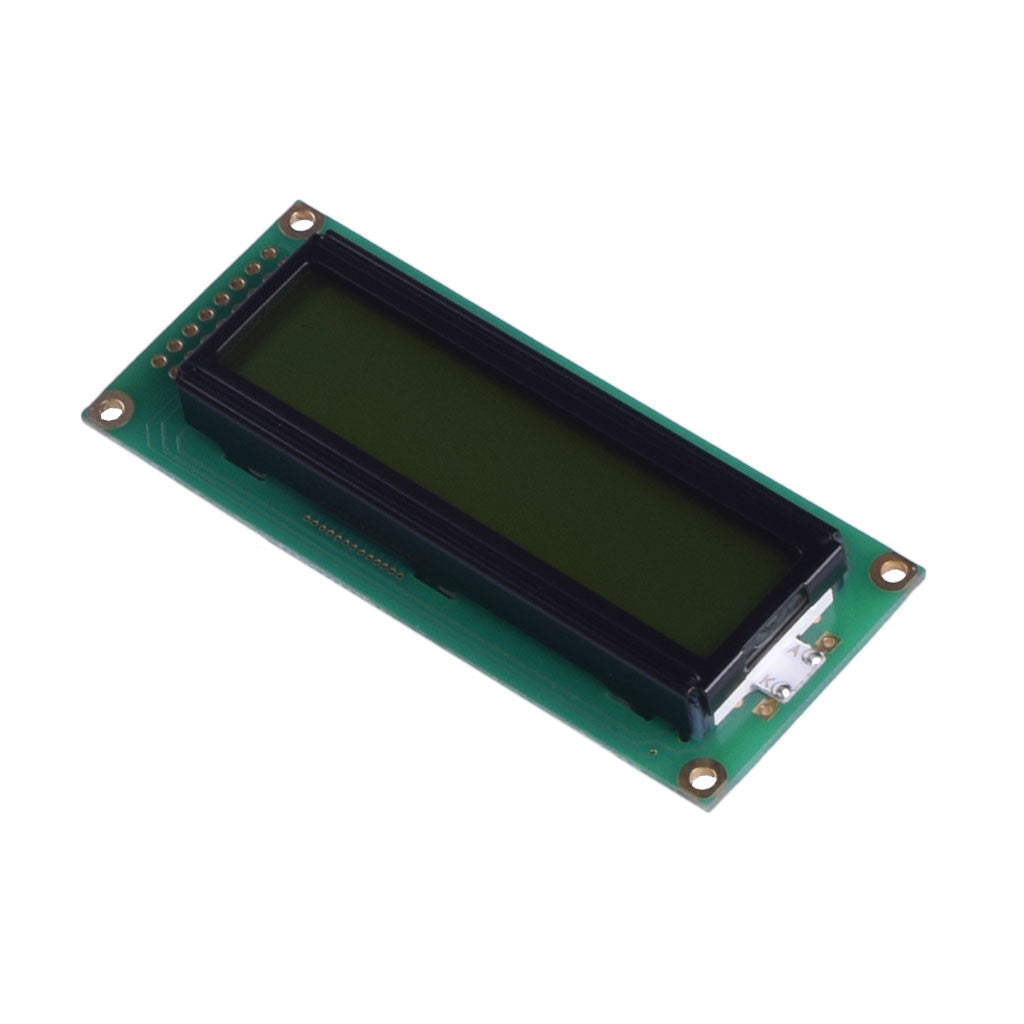
16x2 Character LCD STN Transflective - MCU
- 💹 Enjoy a 20% discount for orders over 500
- 📉 A 15% discount is available for orders ranging from 200 to 499
- 🎁 A 10% discount is available for orders ranging from 50 to 199
- 🎁 A 5% discount is available when ordering 10-49
Interested in customizing this product? Get in touch with us.
Order samples, immediate delivery.
Factory bulk lead time: 3 weeks.
16x2 Character LCD STN Transflective - MCU
- 💹 Enjoy a 20% discount for orders over 500
- 📉 A 15% discount is available for orders ranging from 200 to 499
- 🎁 A 10% discount is available for orders ranging from 50 to 199
- 🎁 A 5% discount is available when ordering 10-49
Resources & Downloads
16×2 Character LCD STN Transflective - MCU
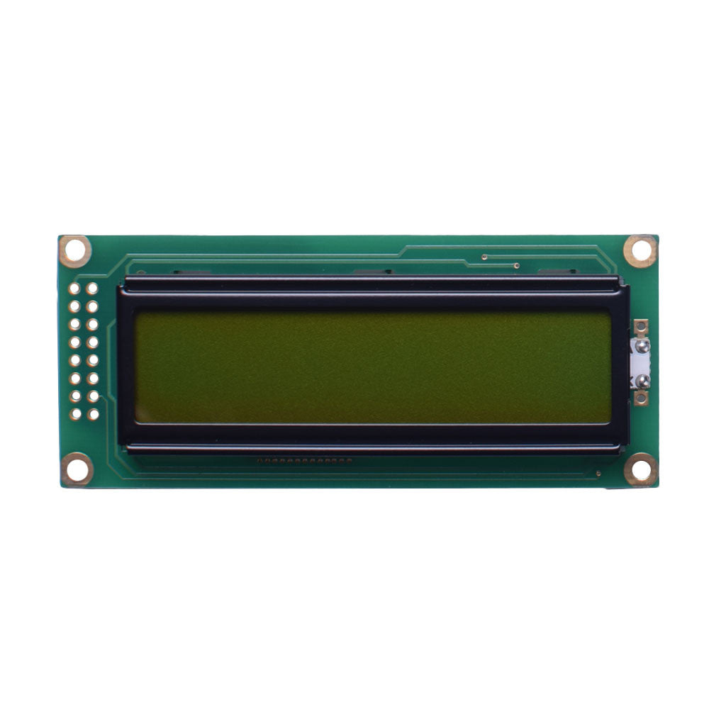
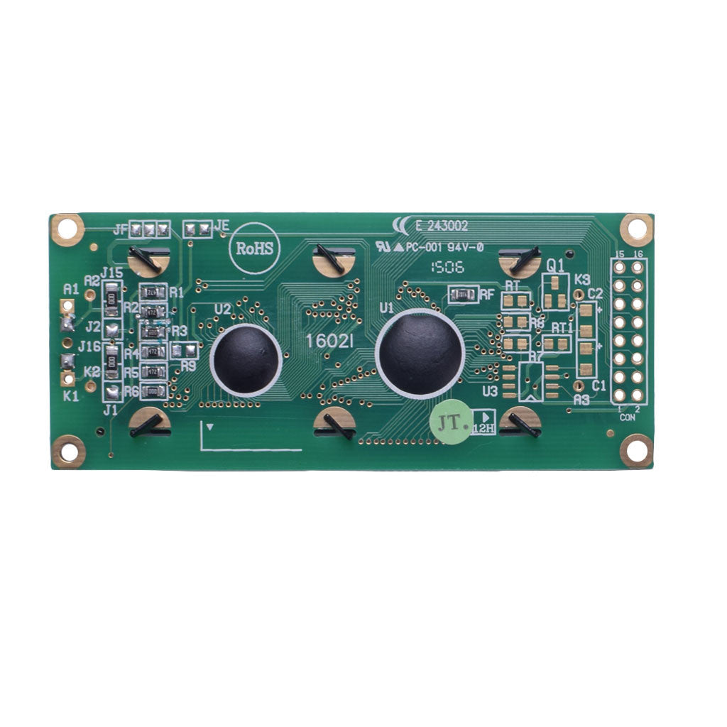
DM-LCD1602-423 is a 16-character by 2-line monochrome LCD module with an STN positive yellow-green transflective display, yellow-green LED backlight, ST7066U controller, and 6800-series parallel MPU interface.
The module uses a nominal 5.0 V logic supply and supports both 4-bit and 8-bit parallel data transfer. Its 85.0×36.0 mm PCB outline, 66.0×16.0 mm viewing area, and 16-pin through-hole connection provide a documented mechanical and electrical platform for alphanumeric equipment interfaces.

Technical Specifications
Electrical, optical, environmental, and mechanical values for the DM-LCD1602-423 module.
The product specification includes the module outline, viewing area, active area, pin assignment, voltage limits, optical data, timing, and reliability conditions.
| Parameter | Specification |
|---|---|
| Product Model | DM-LCD1602-423 |
| Display Type | Monochrome character LCD module |
| Character Format | 16 characters × 2 lines |
| LCD Mode | STN positive, yellow-green, transflective |
| Backlight | Yellow-green LED |
| Controller IC | ST7066U |
| MPU Interface | 6800-series parallel interface |
| Data Bus | 4-bit or 8-bit parallel transfer |
| Character Font Mode | Two-line 5×8-dot character mode |
| Module Dimensions | 85.0×36.0×13.2 mm maximum |
| Viewing Area | 66.0×16.0 mm |
| Active Area | 56.2×11.5 mm |
| Viewing Direction | 6:00 |
| Duty Cycle | 1/16 |
| Nominal Logic Supply | 5.0 V |
| Logic Supply Range | 4.5 V minimum, 5.0 V typical, 5.5 V maximum |
| Logic Supply Current | 1.0 mA minimum, 1.2 mA typical, 1.5 mA maximum at VDD = 5.0 V |
| Backlight Supply Voltage | 3.9 V minimum, 4.1 V typical, 4.3 V maximum |
| Backlight Supply Current | 117 mA minimum, 130 mA typical, 156 mA maximum |
| Operating Temperature | -20°C to +70°C |
| Storage Temperature | -30°C to +80°C |
| Module Weight | 32.8 g |
Optical and Electrical Characteristics
The transflective LCD combines reflected ambient light with the integrated LED backlight. Published optical values are specified under the measurement conditions shown in the module datasheet.
Yellow-Green Transflective LCD
The display is designed for a 6:00 viewing direction. Readability in the finished device is influenced by contrast voltage, operating temperature, ambient illumination, front-window material, and installation angle.
Vertical Viewing Angles
Top viewing angle is 20° typical. Bottom viewing angle is 40° typical.
Horizontal Viewing Angles
Left and right viewing angles are each specified as 30° typical.
Response Time
Combined rise and fall response time is 300 ms typical and 400 ms maximum at 25°C.
Contrast Ratio
The published typical contrast ratio is 3 under the datasheet measurement conditions.
Backlight Luminance
The datasheet specifies 216 cd/m² minimum and 270 cd/m² typical, measured without the LCD.
High-Level Input
The minimum high-level input voltage is 0.7 × VDD. At VDD = 5.0 V, the specified minimum is 3.5 V.
Mechanical Dimensions
The mechanical drawing defines the PCB outline, viewing window, active area, mounting holes, connection pattern, component depth, and dimensional tolerances used for enclosure and host-PCB planning.
PCB-Mounted Character Module
The drawing shows four plated mounting holes, a 2-row by 8-pin through-hole interface, a 1.6 mm PCB thickness, and a 13.2 mm maximum assembled depth.
Pin Assignment and Parallel Interface
The 16-pin through-hole connection provides logic power, LCD contrast control, register selection, read/write control, enable timing, an 8-bit data bus, and separate LED backlight power.
4-Bit and 8-Bit Bus Modes
In 8-bit mode, DB0 through DB7 transfer one complete byte. In 4-bit mode, DB4 through DB7 transfer each byte in two 4-bit operations.
RS selects instruction or display-data access.
R/W selects read or write operation.
E is the chip-enable signal used for bus timing.
A and K provide the separate positive and negative LED backlight connections.
Host Interface Timing
The timing values below apply to module write and read operations through the 6800-series parallel interface.
Enable-Controlled Parallel Transfer
Address, data, and enable timing must satisfy the minimum setup, hold, pulse-width, and cycle-time limits for reliable command and display-data transfer.
ST7066U Display Functions
The ST7066U provides display memory, character generation, instruction decoding, cursor control, and LCD drive functions. The DM-LCD1602-423 uses the controller in two-line 5×8-dot mode with a 1/16 duty cycle.
Integrated Character Control
The controller contains the display RAM, character ROM, custom-character RAM, command logic, cursor, blink, and parallel MPU interface required by the module.
Character ROM
The ST7066U includes a 13,200-bit character generator ROM with 240 character fonts.
Custom Characters
The 64×8-bit CGRAM supports eight programmable 5×8-dot character patterns.
Display Commands
Functions include clear, cursor home, display on/off, cursor control, blink, entry mode, and display shift.
Display Memory
The controller includes 80×8-bit DDRAM. Visible addresses are 00H-0FH on line 1 and 40H-4FH on line 2.
Environmental and Reliability Conditions
The module specification includes storage, powered operation, humidity, thermal-shock, vibration, and static-electricity test conditions for engineering review.
Engineering Integration Notes
Apply the published voltage, input-level, timing, backlight, contrast, initialization, and mechanical limits when designing the host circuit and enclosure.
Separate Logic, Contrast, and Backlight Requirements
The logic supply, LCD contrast input, and LED backlight have different electrical functions and published limits. They should be implemented according to the module circuit and electrical tables.
Logic supply: Operate VDD within the specified 4.5-5.5 V range.
Host logic level: At VDD = 5.0 V, the published minimum high-level input is 3.5 V.
Backlight supply: Design the LED supply for the specified 3.9-4.3 V range and 130 mA typical current.
Contrast control: The module block diagram shows VO adjustment using an external 10-20 kΩ variable resistor between VDD and VSS.
4-bit bus: Use DB4 through DB7 and transfer each byte in two 4-bit operations.
8-bit bus: Use DB0 through DB7 for complete byte transfers.
Power-on sequence: Use the specified initialization procedure for the selected 4-bit or 8-bit interface.
Busy flag: When DB7 reports the busy flag as high, the controller is processing the previous instruction.
Enclosure design: Allow for the 13.2 mm maximum depth, mounting pads, pin clearance, viewing area, and 6:00 viewing direction.
Character content: Match the controller character-ROM version to the language and symbols required by the finished interface.
Common Questions
Does the module support 4-bit communication?
Yes. In 4-bit mode, DB4 through DB7 transfer each 8-bit instruction or data byte in two operations.
Does a 3.3 V host meet the input specification?
The module specifies VIH as at least 0.7 × VDD. With VDD at 5.0 V, the specified minimum high-level input is 3.5 V.
Is the backlight powered from the same voltage as VDD?
The logic supply is specified at 4.5-5.5 V. The separate LED backlight supply is specified at 3.9-4.3 V and 130 mA typical.
How is display contrast adjusted?
VO is the variable LCD operating-voltage input. The module block diagram shows an external 10-20 kΩ variable resistor connected between VDD and VSS.
Can custom symbols be displayed?
Yes. In the two-line 5×8-dot mode, the controller CGRAM supports eight programmable character patterns.
What is the visible memory address range?
The 16 visible positions on line 1 use DDRAM addresses 00H-0FH. The 16 visible positions on line 2 use addresses 40H-4FH.
What does the luminance value represent?
The published 216 cd/m² minimum and 270 cd/m² typical values are backlight luminance measurements taken without the LCD.
Which dimensions affect enclosure design?
Use the 85.0×36.0 mm PCB outline, 13.2 mm maximum depth, 66.0×16.0 mm viewing area, 80.0×31.0 mm mounting centers, and pin-clearance dimensions.
Download Technical Documents
Review the module datasheet for dimensions, electrical characteristics, optical data, pin assignment, timing, initialization, font table, and reliability conditions.
Use the ST7066U controller datasheet for controller architecture, instruction functions, bus operation, memory organization, and detailed electrical timing.