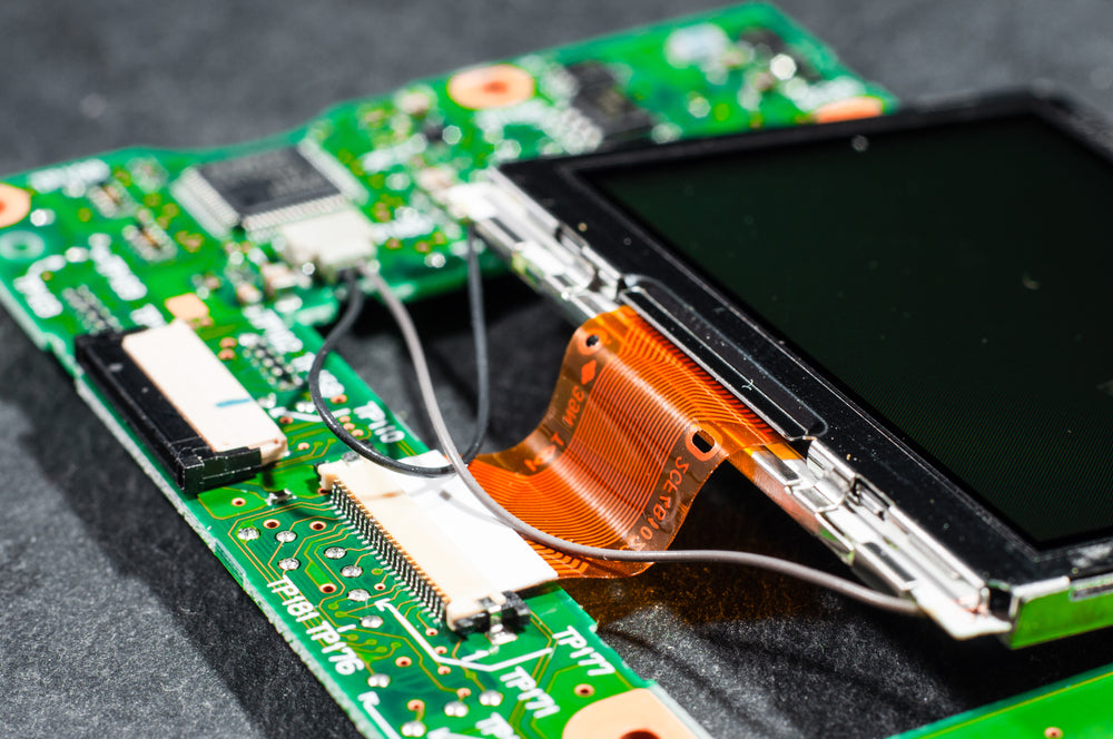
The Pad Area, also known as the Bonding Area, is a crucial part of the LCD (Liquid Crystal Display) structure where the electrodes on the array glass substrate connect with the peripheral driving integrated circuits (ICs). This area ensures that the electrical signals necessary for driving the display are accurately transmitted.
Connection Methods
There are three common methods used to achieve this connection:
1. COF (Chip-on-Film):
• Usage: Primarily used for large-sized displays.
• Description: Involves mounting the driving ICs onto a flexible film which is then connected to the glass substrate. This method allows for a robust and flexible connection that can accommodate the larger dimensions of big screens.
2. COG (Chip-on-Glass):
• Usage: Suitable for medium and small-sized displays.
• Description: Involves directly mounting the driving ICs onto the glass substrate. This method is ideal for compact displays as it minimizes space and ensures a strong, stable connection.
3. FOG (Film-on-Glass):
• Description: Involves connecting flexible printed circuits (FPCs) to the glass substrate, often used in conjunction with COG to achieve circuit connectivity.
Distribution Based on Panel Driving Architecture
The distribution of the pad area varies depending on the panel driving architecture:
• All Four Sides: Pads are distributed around the entire perimeter of the panel.
• Three Sides: Pads are distributed along three sides—two sides for scanning pads and one side for data pads.
• One Side (GOA Driving Architecture): Pads are distributed along only one side, with all the data pads located on this side.
Each pad area typically contains multiple pads, and each pad corresponds to a COF, COG, or FPC. These connections are made using anisotropic conductive film (ACF), which contains conductive particles such as gold balls to ensure electrical connectivity.
Structure and Function of the Pad Area
In a typical pad structure connected to a COF, each pad includes:
1. A Row of Electrodes:
• Channel Electrode Area: These electrodes connect to the data lines or scan lines of the display.
• Function Electrode Area: These electrodes are associated with various control signal lines and common electrode lines relevant to scanning and driving functions.
2. Alignment Marks:
• Marks: These are used to align the COF with the pad area during the bonding process. Proper alignment is critical to ensure reliable electrical connections and optimal display performance.
3. Virtual Electrodes:
• Purpose: Located at the edges of the pad area, these virtual electrodes help assess the bonding quality. They provide a reference to check the compression state of the gold balls within the ACF, ensuring that the electrical connections are secure and functional.
Importance of the Pad Area
The pad area is essential for several reasons:
• Signal Transmission: It facilitates the precise transmission of electrical signals between the driving ICs and the display panel.
• Structural Integrity: Proper bonding ensures that the display is structurally stable and resistant to mechanical stresses.
• Performance: Accurate alignment and reliable connections contribute to the display’s overall performance, including image quality, response time, and durability.
Read more

The sealing area in a liquid crystal display (LCD) is the region extending from the boundary of the active display area to either the pad area or the cutting edge of the glass substrate. This area...

Liquid Crystal Displays (LCDs) employ various display modes, each with unique pixel structures and design intricacies. The most common modes include: • Twist Nematic (TN) Mode: Known for its fa...


Leave a comment
This site is protected by hCaptcha and the hCaptcha Privacy Policy and Terms of Service apply.