


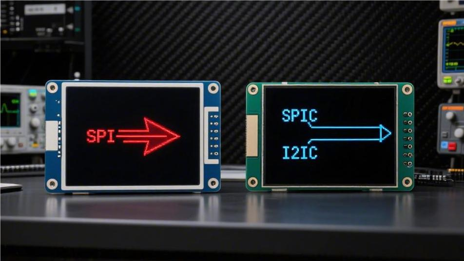
SPI vs I2C Display Interfaces | Speed & Use Cases
The SPI display interface requires 4 wires and can reach frequencies of 50MHz or higher, making it suitable for driving color TFT screens to smoothly play animations.
The I2C interface, on the other hand, only needs to connect two wires, SDA and SCL, with a speed typically limited to 400kHz, making it more suitable for driving a 0.96-inch monochrome OLED screen to display static text.
Speed
The operating frequency of the I2C standard mode is 100kHz, and the fast mode is 400kHz.
It adopts an open-drain output. Transmitting a single frame of 128x64 monochrome data (about 1KB), including the device address and ACK response, takes approximately 25 milliseconds.
SPI adopts a push-pull output, without addressing and acknowledgment bits, and the clock frequency is usually set between 10MHz and 50MHz.
At 20MHz, it takes SPI about 61 milliseconds to transmit one frame of 320x240 resolution 16-bit color data (153.6KB).
The physical clock difference between the two is more than 50 times. I2C handles small volumes of static data, while SPI is used to output high frame rate color images.
Level Transition Speed
The internal circuit structure of the physical pins sets the physical upper limit of the signal frequency. A microcontroller sending data to a display screen essentially switches the voltage on the wires back and forth between 0V and 3.3V.
The wires and the receiving pins of the display panel generate parasitic capacitance. A 20-centimeter-long 24AWG connection wire has a physical capacitance of about 20pF to 30pF.
The I2C bus adopts an open-drain output structure. When the microcontroller needs to output a low level, the internal N-channel MOSFET turns on, forcing the bus voltage to 0V, which takes only a few nanoseconds.
When a 3.3V high level is needed, the microcontroller turns off the internal transistor, cutting off the level control to the bus. At this time, it relies on the externally connected pull-up resistor to slowly pull the bus voltage high.
The current must charge the parasitic capacitance on the entire bus through a pull-up resistor (commonly 4.7kΩ or 2.2kΩ). This process forms a standard RC charging circuit.
-
The pull-up resistor is 4.7kΩ
-
The bus parasitic capacitance is estimated at 100pF
-
The RC time constant is about 470 nanoseconds
-
The voltage takes about 1 microsecond to reach the target level
In the 400kHz fast operating mode, a complete clock cycle is only 2.5 microseconds. The high-level state occupies half of this time, which is 1.25 microseconds.
The 1 microsecond spent charging the capacitor occupies 80% of the high-level time window. When connecting a logic analyzer to measure the I2C SDA pin, the screen displays a sawtooth waveform with a very long rising slope.
If the I2C clock frequency is forcefully increased to 1MHz, half a cycle is shortened to 0.5 microseconds. At this point, before the capacitor is charged to the lowest threshold recognized by the microcontroller (usually 70% of VDD, i.e., 2.31V), the next low-level signal has already arrived.
The display control chip will read a continuous string of erroneous low-level data. To shorten the charging time, one can only reduce the physical resistance value of the pull-up resistor.
Lowering the resistance to 1kΩ will increase the current flowing through when the chip pulls down to 0V. The I2C specification states that the maximum sink current cannot exceed 3 milliamperes; too small a resistance will burn out internal physical components.
The SPI interface discards the pull-up resistor charging mechanism. Its SCK clock line and MOSI data line completely adopt a push-pull output physical structure.
The microcontroller is internally configured with a pair of complementary transistors. The N-channel transistor operates when outputting a low level, and the P-channel transistor actively injects physical current into the bus when outputting a high level.
The push-pull output impedance of the main control chip is extremely low, usually between 20Ω and 50Ω. Facing the same 100pF parasitic capacitance, the RC time constant is sharply compressed to 2.5 nanoseconds.
-
Push-pull output impedance is calculated at 30Ω
-
The charge and discharge time constant is about 3 nanoseconds
-
The physical time consumption of the rising edge is extremely short
-
Free from the constraints of external pull-up resistors
It takes less than 10 nanoseconds for the voltage to soar from 0V to 3.3V. The oscilloscope screen displays a standard square wave with vertical edges and clear black-and-white contrast.
Under a 50MHz SPI clock frequency, one clock cycle is 20 nanoseconds, with a high-level window of 10 nanoseconds. The push-pull structure can complete the level transition in 2 to 3 nanoseconds, giving the display control chip at least 7 nanoseconds to accurately sample the digital bits.
Long-distance wiring will multiply the parasitic capacitance of physical lines. In complex hardware engineering environments, the impact of capacitance changes caused by wire length on the physical attenuation of different interfaces varies tremendously.
A 1-meter-long ribbon cable introduces about 150pF of extra capacitance. When I2C faces a highly capacitive load, the rising edge of the waveform is severely elongated, and the original 400kHz frequency must be reduced to 100kHz to prevent packet loss.
-
Increased wire length pushes up physical capacitance
-
I2C waveform distortion becomes extremely severe
-
Communication frequency is forced to step down and decelerate
-
SPI has an extremely strong resistance to capacitive loads
Facing a 150pF parasitic load, the push-pull output SPI can still maintain a clear square wave shape at a frequency of 10MHz (100 nanoseconds cycle), even if the rise time increases to 15 nanoseconds. SPI can transmit high-resolution color data through longer physical cables at the expense of very little frequency.
Data Packing Steps
When a communication protocol transmits payloads over physical cables, it must attach extra control bits such as addressing and status verification. Before the microcontroller sends a byte of color data, the bus needs to consume additional clock cycles to establish transmission rules.
Multiple physical devices are mounted on the I2C bus, and it relies on address broadcasting on the bus to wake up the specified display chip. The master control pin pulls down the SDA line to generate a Start bit, which occupies 1 clock cycle.
Subsequently, the microcontroller sends a 7-bit slave device address (such as 0x3C commonly used for OLED) in a most-significant-bit-first order, followed by 1 read/write control bit (0 for a write operation). This constitutes the first 8-bit control frame.
The protocol requires the receiving party to pull down the SDA line in the 9th clock cycle to issue an ACK response. If there is no response, the master controller defaults to the device being offline and terminates communication.
After sending the address, the microcontroller also needs to send a 1-byte register address to inform the display chip whether the data should be written to RAM or the command register. This consumes another 8 data bits and 1 ACK response bit.
The bus has already run for 18 clock cycles without transmitting a single pixel point of an effective frame. It is not until the 19th cycle that the screen's first color data byte begins to enter the physical bus.
In continuous burst write (Burst Write) mode, I2C allows continuous transmission of image data after a single addressing. For every 8 bits of color data transmitted, 1 ACK bit issued by the screen chip is still forcibly interleaved.
-
Effective data is fixed at 8 bits
-
Mandatory binding of 1 ACK verification bit
-
A single byte physically occupies 9 cycles
-
Protocol payload efficiency is only 88.8%
Refreshing a 128x64 resolution monochrome screen totals 1024 bytes of effective payload. In continuous write mode, 9216 bits are physically transmitted on the I2C bus, plus start, address, and stop bits.
At a 400kHz clock frequency, transmitting these 9216 bits takes 23.04 milliseconds. Among this, the verification ACK response bits alone occupy more than 2.5 milliseconds of pure physical transmission time.
The SPI bus discards the in-band addressing and acknowledgment mechanism. It manages the intervention timing and data attributes of communication devices through the level status of physical pins.
The microcontroller pulls down the CS (Chip Select) pin connected to the screen to 0V; the display chip is immediately awakened and ready to receive the bitstream. While the 0V state is maintained, signals on the bus belong exclusively to that screen.
An independent D/C (Data/Command) pin is responsible for distinguishing payload types. A 3.3V high level indicates that subsequent data entering are RGB pixels, while a 0V low level indicates that they are brightness or contrast adjustment parameters.
-
The CS pin replaces the 7-bit device address
-
The D/C pin replaces the register pointer
-
Completely eliminates the ACK waiting mechanism
-
The bus pours out effective pixels at full load
Physical pins divert the pressure of logical judgment. Clock cycles on the MOSI data line achieve 100% payload transmission, with 8 cycles precisely corresponding to 8 bits of image data.
Facing a 320x240 resolution 16-bit color screen, a single frame contains 153,600 bytes. The SPI bus only needs to pull down the CS and D/C pins once before the first byte.
Relying on the DMA (Direct Memory Access) controller, the microcontroller continuously sends 1,228,800 bits. Under a 20MHz SPI clock, 1.22 million data bits race through a single physical channel.
After 61.44 milliseconds, the transmission of the 153.6KB single frame image is complete. The microcontroller pulls the CS pin high to 3.3V, and a complete full-screen refresh action concludes in microsecond-level latency.
If the same 153.6KB of data were to be transmitted via I2C, the forcibly inserted ACK bits in burst mode would reach 153,600. The attached verification bits alone would take up an additional 384 milliseconds of communication time.
The refresh rate of a screen cannot tolerate hundreds of milliseconds of protocol overhead delay. SPI's transmission approaches zero-burden raw stream direct writing, and the independent division of labor among physical pins avoids bits queuing up on a single wire.
SRAM controllers inside high-resolution panels are generally designed with automatic address increments. While the SPI's CS signal remains low, for every 8 pulses received, the hardware pointer automatically shifts right by one bit without microcontroller intervention.
I2C's half-duplex design requires the bus to constantly switch pin input and output directions between the master's transmission and the slave's ACK response. The direction switching of a microcontroller's GPIO register typically consumes 2 to 3 CPU instruction cycles.
Based on a 72MHz ARM Cortex-M3 processor, 3 instruction cycles take about 41 nanoseconds. 150,000 ACK responses will generate more than 6 milliseconds of pure CPU wait time, exacerbating the bus's idle rate.
SPI's unidirectional MOSI output design eliminates the electrical action of switching pin directions. Data is fed unidirectionally from the microcontroller's transmit shift register into the display panel's receive buffer, with no hardware handshake obstructions in between.
Real-world Screen Refresh Time
The control chip maps the received binary bits to luminous pixel points on the physical screen. A 128x64 resolution monochrome OLED panel contains 8192 physical pixels, driven by the SSD1306 chip. Each pixel only has two states, bright and dark, occupying 1 bit, and a single complete frame exactly corresponds to 1024 bytes of video memory data.
The microcontroller uses the 400kHz fast mode to send 1024 bytes to the chip. Adding the 9 bits per byte protocol-attached response bit, 9216 clock cycles run on the physical bus. The single frame transmission takes about 23 milliseconds in pure physical time, theoretically allowing for 43 full-screen refreshes per second.
A refresh rate of 43 FPS exceeds the 24 FPS threshold of human visual persistence. Scrolling numbers and basic progress bar animations on the screen can remain continuous without producing ghosting. If the dozens of microseconds of CPU processing delay are factored in, the actual frame rate will stabilize at around 35 FPS.
Switching to a hardware SPI bus at a 10MHz operating frequency to drive the same panel, the 1024-byte single-frame data translates into 8192 continuous clock pulses. At 10MHz frequency, each cycle is 100 nanoseconds, compressing the overall transmission time to 819 microseconds.
| Interface Type | Operating Frequency | Bits Per Frame | Transmission Time | Theoretical Max FPS |
|---|---|---|---|---|
| I2C Fast Mode | 400 kHz | 9,216 bits | ~23 ms | ~43 FPS |
| I2C Fast Mode Plus | 1 MHz | 9,216 bits | ~9.2 ms | ~108 FPS |
| Standard SPI | 10 MHz | 8,192 bits | ~0.8 ms | >1000 FPS |
A transmission time of less than 1 millisecond shifts the screen's physical refresh bottleneck to the response speed of the OLED material itself. The microcontroller can clear and rewrite the entire video memory within 1 millisecond, leaving over 99% of the idle time window for processing sensor floating-point calculations.
A 2.4-inch TFT color LCD screen is usually equipped with the ILI9341 driving chip, pushing the physical resolution to 320x240. When using the RGB565 format, each pixel point requires 16 bits to describe the red, green, and blue color ratio. The entire panel's single frame data volume drastically increases to 153,600 bytes.
If the 400kHz frequency bus is still used to push the 153.6KB of data, a total of 1,382,400 clock pulses are needed along with the ACK bits. The transmission time for a single image stretches to 3.45 seconds. The human eye will clearly perceive the slow scanning process as the picture overwrites from top to bottom, row by row.
The lengthy 3.45 seconds transmission time kills any possibility for dynamic UI interaction. When a user presses a physical button to switch menus, the new frame's image data sent by the microcontroller is still queuing on the wires. The top half of the screen will display the new menu, while the bottom half remains stuck on the old interface, creating severe screen tearing.
| Communication Bus Config | RGB565 Frame Size | Actual Bits Sent | Full Refresh Time | Visual Presentation State |
|---|---|---|---|---|
| 400kHz I2C | 153.6 KB | 1,382,400 | 3456.0 ms | Slow progressive scan |
| 10MHz SPI | 153.6 KB | 1,228,800 | 122.8 ms | Noticeable stutter and tearing |
| 20MHz SPI | 153.6 KB | 1,228,800 | 61.4 ms | Basic smooth sliding |
| 40MHz SPI | 153.6 KB | 1,228,800 | 30.7 ms | Seamlessly silky animation |
Increasing the hardware clock frequency to 20MHz reduces the transmission time of a 153.6KB single frame data to 61.4 milliseconds. With the theoretical frame rate reaching 16 FPS, the microprocessor can support a dashboard UI interface with simple transition animations.
Some microcontrollers using the Cortex-M4 core support clock dividers up to 40MHz or even 50MHz. At 40MHz frequency, 1.22 million data bits pour into the ILI9341's SRAM video memory within 30.7 milliseconds. A refresh rate of 32 FPS is sufficient to play compressed low-resolution video files.
Used in conjunction with the microprocessor's Direct Memory Access (DMA) channel, arrays within the memory are automatically and sequentially moved by the hardware circuit to the MOSI pin output register. When running at a full 40MHz load, CPU utilization stays below 5%, allowing it to simultaneously read the raw image stream of the next frame from external storage.
To reduce communication bandwidth occupation, GUI graphics libraries usually adopt a partial refresh algorithm. When a digit on the screen jumps from 9 to 0, the code only calculates the 32x32 pixel rectangular area occupied by that number. The data volume of the color to be sent drops sharply from 153.6KB to just 2048 bytes.
Faced with a 2048-byte local data block, a 20MHz frequency only takes 100 microseconds to complete the rewrite. Even using 400kHz transmission, the time consumed can be controlled to around 46 milliseconds. Rendering optimization on the software level allows low-speed communication protocols to barely cope with basic color value changes.
However, the physical bandwidth gap cannot be bridged purely by software algorithms. When dealing with a full-screen background image swap or complex page sliding transitions, partial algorithms fail. The video memory requires complete overwriting, and the clock frequency once again becomes the deciding physical constant for whether the panel can respond on time.
When the physical resolution increases to 480x320, the single frame RGB565 volume reaches 307.2KB. The single frame time for a 40MHz bus increases to 61.4 milliseconds, and the frame rate drops to 16 FPS. At this point, serial communication touches the edge of the physical antenna effect, and engineering design must pivot to a parallel 8080 interface or an RGB interface.
Use Cases
Selecting I2C or SPI depends on the microcontroller's GPIO pin count and the screen resolution.
I2C only occupies 2 wires and transmits about 40KB of data per second at a frequency of 400kHz, fulfilling the 1KB single-frame requirement of a 128x64 monochrome OLED, making it suitable for temperature and humidity reading outputs.
SPI utilizes 4 to 6 wires, with clock frequencies generally exceeding 40MHz. When coping with a 320x240 resolution, 16-bit color TFT screen, the single-frame data reaches 153.6KB.
Relying on SPI's tens of Mbps of physical bandwidth, the screen refresh rate stabilizes at over 30fps, fulfilling the physical requirements to run a Graphical User Interface (GUI).
Hardware Specification Comparison
I2C relies on an Open-Drain output architecture. The signal lines SDA and SCL are connected to a 3.3V or 5V power supply via external pull-up resistors. When the bus is in an idle state, it relies on these resistors to maintain both lines at a high physical potential.
The master control chip does not proactively output high levels; instead, it generates low levels by grounding the line through internal transistors. When flipping from low to high level, the power supply charges the parasitic capacitance on the bus through a 4.7kΩ resistor.
The RC time constant restricts the physical speed of the level transition. The I2C bus specification strictly limits the parasitic capacitance to 400pF. Connecting too many slave devices or having cables longer than 30 centimeters will cause the edges of the square wave signals to flatten out.
-
Pin assignment: SDA (Data) and SCL (Clock)
-
Output topology: Open-drain connection
-
Required components: 2.2kΩ to 10kΩ pull-up resistors
-
Capacitive load: Maximum 400pF limitation
-
Bus level: Supply voltage (VDD) when idle
The I2C protocol specifies a clock frequency of 100kHz in standard mode, and bumps it up to 400kHz in Fast Mode. The physical throughput cap at 400kHz is 400,000 bits per second.
Data is transmitted in 8-bit byte packages on the I2C bus. The receiver must send an acknowledgment bit (ACK) pulling the level low during the 9th clock cycle. With additional start and stop bits, a single byte transmission consumes 10 to 11 clock cycles.
Protocol overhead cuts into the actual transmission bandwidth. The effective data payload rate for I2C at 400kHz is roughly 36KB per second. Transmitting a 128x64 pixel monochrome BMP image (1024 bytes total) physically takes around 28 milliseconds.
SPI adopts a Push-Pull output design. The transistors inside the master controller alternately conduct, forcing the level high to 3.3V or low to 0V. The output current provided by push-pull circuits is usually in the range of 10mA to 20mA.
This high current output capability negates the need for external pull-up resistors, making the rising and falling edges of the signals extremely steep. A microcontroller's (like the ATmega328P) SPI clock can be configured up to 8MHz, while hardware like the ESP32 supports frequencies up to 80MHz.
-
Pin composition: MOSI, MISO, SCK, CS
-
Output topology: Push-pull output structure
-
Operating mechanism: Master proactively outputs high/low levels
-
Frequency limit: Determined by the microcontroller's internal clock divider
-
Protocol consumption: No hardware acknowledgment bit (ACK) delays
I2C uses a 7-bit or 10-bit software addressing mechanism. The master broadcasts the hexadecimal address during the communication startup phase. For instance, 0x3C corresponds to the OLED controller IC SSD1306; every device on the bus will listen to the addressing byte at the header of the data packet.
Software addressing allows I2C to hook up to as many as 128 independent components using just two pins. The microcontroller's GPIO pin occupation rate drops incredibly low, which is ideal for miniature processors like the ATtiny85 that possess only 8 pins in total.
SPI scraps software addressing and uses a purely hardware-based Chip Select line (CS or SS). The master must allocate a separate dedicated GPIO physical pin to every single display screen connected to the bus.
When writing data to a specific screen, the microcontroller pulls the voltage level of the corresponding CS pin down to 0V. The screen's control IC is then awakened and begins receiving the synchronous data stream coming in from the MOSI pin.
When lighting up a color TFT LCD screen, conventional 4-wire SPI typically adds two extra pins: DC (Data/Command selection line) and RST (Hardware Reset line).
When the DC pin is at a 0V low level, the data transmitted on MOSI is interpreted by display controller ICs like the ILI9341 as hexadecimal commands for configuring registers. When the DC pin is set to a 3.3V high level, subsequent data is stored into internal GRAM as pixel color blocks.
Eliminating software protocol parsing reduces video memory write latency. Hardware-level pin switching, paired with a 40MHz SCK square wave, allows 16-bit RGB565 format image data to be poured into the screen at tens of megabytes per second.
-
MOSI: Transmits commands or pixel color data
-
SCK: Generates a high-frequency square wave for synchronous data reading
-
CS: Zero-volt low level activates the display screen control IC
-
DC: High level designated as data, low level designated as command
-
RST: Low-level pulse executes a hardware-level reset of the screen
The high-frequency SPI signals from the push-pull output are incredibly sensitive to line impedance. If the SCK frequency is set at 40MHz and a jumper wire longer than 10 centimeters is used, signal reflection and crosstalk will result in white screens or snow-like noise on the display.
Ensuring high-frequency signal integrity requires hardware-level intervention. SPI display screens usually utilize extremely short FPC flexible flat cables soldered directly to the main PCB, with 22Ω to 33Ω impedance-matching terminating resistors wired in series onto the MOSI and SCK traces.
I2C is far more physically forgiving regarding trace lengths. At a 100kHz rate, by swapping the pull-up resistor to a 2.2kΩ one to increase the bus sink current, an I2C monochrome screen can stably receive commands through a three-core cable up to 50 centimeters long.
Low-Speed Text Scenarios
When a microcontroller communicates with peripherals, a 100kHz I2C bus can transmit about 10,000 bytes of effective payload per second. On a 0.96-inch monochrome OLED screen with a resolution of 128x64 pixels, completely refreshing a single frame takes 1024 bytes of video memory.
In the 400kHz Fast Mode, the theoretical maximum allows the microcontroller to push nearly 40 frames per second to the SSD1306 driver IC. Human visual perception has extremely high tolerance for static numbers and letters updating; environmental monitoring devices that set their refresh rates to 2Hz easily meet visual reading demands.
-
1602 LCD module: Built-in HD44780 controller, single screen physically houses 32 independent 5x8 pixel dot matrix ASCII characters
-
2004 LCD module: 4-row display layout, single screen physically houses 80 independent characters, equipped with a 5V yellow-green LED backlight
-
0.91-inch OLED: 128x32 pixel matrix, adapted for narrow PCB trace spaces with a width of just 12 mm
Old-school 1602 LCD screens originally required occupying at least 6 of the microcontroller's GPIO pins (RS, EN, and D4 through D7). Engineers typically solder an I2C adapter board carrying a PCF8574 chip onto the back of the screen, downshifting the 8-bit parallel communication into a 2-wire serial format.
The PCF8574 chip acts as an 8-bit I/O expander. It listens for the 0x27 hex address on the SDA line, converts the serial bytes sent by the microcontroller into 3.3V or 5V parallel level signals, and synchronously pushes them out to the LCD's pin headers.
The two-wire system eliminates the electromagnetic risks of crosstalk between multiple high-frequency lines at the PCB routing level. The Arduino UNO board, based on the ATmega328P chip, has a grand total of only 14 digital pins; complex mechanical stepper motor control projects can easily exhaust this entire stockpile of digital pins.
SDA and SCL pins allow the physical parallel connection of multiple slave devices with different hardware addresses. In a weather station project, a BME280 temperature and humidity sensor (factory address 0x76) and a monochrome OLED screen (factory address 0x3C) share the very same bus network consisting of the A4 and A5 analog pins.
-
Physical time for reading barometric pressure data: ~2 milliseconds (transmitting a 16-bit data packet + ACK bit)
-
Temperature data extraction mechanism: Continuously reading three 8-bit bytes starting from the 0xFA register address
-
Screen pixel dot matrix write mode: Based on Page Addressing, treating every vertical column of 8 pixels as a single unit
Within its main loop code, the microcontroller first sends a request byte to address 0x76 to acquire a 20-bit resolution physical level reading of the environmental temperature. Upon capturing the reading, the bus level is reset by the slave, and the microcontroller immediately generates a falling-edge start signal containing address 0x3C.
After converting the temperature variable into its corresponding hex array from the ASCII map, the MCU pushes the 8x16 pixel font matrix array page by page into the Static Random Access Memory (SRAM) inside the OLED. The display driver's row and column selection circuits light up the organic light-emitting diodes based on the level flip states within the SRAM.
Compared to the steady-state current drain of up to 150mA for full-color screens equipped with LED backlights, a 0.96-inch OLED consumes only 10mA to 15mA of current for the entire board when displaying 20 standard text characters. Ripple fluctuations on the system's 5V power network are suppressed to an incredibly low level.
These ultra-low power physical metrics perfectly align with the battery supply demands of portable measuring instruments. A wireless thermometer/hygrometer powered directly by a single 18650 lithium battery (nominal 3.7V, 2600mAh capacity), keeping the screen constantly on and updating sensor readings every minute, can continuously operate for over 300 hours.
Protocol headers, hardware acknowledgment bits (ACK), and Start/Stop level conditions take up nearly a quarter of I2C communication's physical bandwidth. When a microcontroller sends 10 payload bytes of text data to the screen consecutively, the actual number of clock square-wave pulses generated on the SCL line easily exceeds 100.
-
0x00 control byte flag: Indicates that the subsequent payload sent by the MCU is a register command to configure screen contrast
-
0x40 control byte flag: Indicates that the subsequent payload is graphical dot matrix data needing to be pushed to the physical pixel array
-
Column address reset command: Sending the two-byte combination of 0x00 and 0x10 to force the video memory pointer back to the leftmost pixel
The physical structure of the video memory restricts monochrome OLEDs to vertical block overwriting in chunks 8 pixels high. When the panel of a miniature instrument needs to update just the third letter on the first line independently, the MCU must send a 6-byte physical positioning command containing the column start address to the screen.
Partial pixel refresh technology circumvents the extended bus pin occupation that a full 1024-byte screen overwrite would cause. By solely updating a 16x16 pixel weather status icon, the microcontroller takes less than 4 milliseconds under a 100kHz clock to free up the SDA data line.
After releasing the communication bus, the distributed capacitance on the SDA line is charged by the 4.7kΩ pull-up resistor, smoothly raising the level back to 3.3V. An EEPROM memory chip (physical address 0x50) residing on the same PCB can then seamlessly join the network, relaying historical temperature log snapshots back to the MCU.
I2C bus specifications heavily enforce that parasitic capacitance on the lines must be capped under a physical threshold of 400pF. Should the sensor and screen be located over 30 centimeters away from the microcontroller, the edges of the square-wave signals will become profoundly smoothed out, leading the MCU's hardware TWI module to incorrectly identify the high/low level flipping thresholds.
This physical ceiling of sub-400kHz clock square waves entirely blocks any path toward implementing high-framerate progressive scan animations. Monochrome text, discrete geometric lines, and dot matrix icons up to 16x16 pixels constitute the absolute data throughput ceiling for open-drain 2-wire communication strictly confined under 400pF capacitive load constraints.
High-Speed Full-Color Scenarios
The push-pull output architecture empowers microcontroller pins to actively pump out a 3.3V high level and a 0V low level, breaking free from the physical constraints the RC time constant places on level flipping rates. After configuring the hardware SPI channel's clock divider on microprocessors like the ESP32-S3, the square wave frequency generated at the SCK pin runs as high as 80MHz. The physical duration of a single clock cycle compresses down to a staggering 12.5 nanoseconds; coupled with the full-duplex MOSI data line, it can blast out over 10MB of pure payload pixel level pulses to peripherals every second. When stepping up screen resolution from a monochrome 128x64 to a 2.4-inch, 240x320 full-color TFT, the color depth for a single pixel expands into a 16-bit physical storage requirement.
Under the RGB565 color format standard, red occupies 5 bits, green 6 bits, and blue 5 bits, obligating 2 bytes of Static Random Access Memory (SRAM) space just to light up a single colored pixel. To fill the entire internal GRAM space of a 2.4-inch, 240x320 resolution screen, a single full-screen overwrite requires the MCU to pump 153,600 physical bytes (roughly 150KB) consecutively. To maintain a visually seamless 30fps video-grade fluidity, the microcontroller has to continuously blast up to 4,608,000 bytes of hexadecimal data streams into the display chip every 1000 milliseconds.
The High-Speed Serial Peripheral Interface avoids the bandwidth penalty inflicted by broadcasting slave hexadecimal addresses, opting instead for dedicated GPIO physical pins executing point-to-point hardware handshakes. The moment the microcontroller pulls the chip select (CS) pin down to 0V, the designated screen's internal IC wakes up and starts listening. The data/command select (DC) pin dictates the incoming MOSI data stream's properties purely on an electrical hardware level. When the microcontroller drives the DC pin low, hex bytes like 0x2A and 0x2B traveling on the MOSI line get decoded via hardware to become boundary pointers establishing the X and Y axes within the video memory.
The MCU then rapidly thrusts the DC pin back up into a 3.3V high state; the millions of consecutive high and low level pulses rocketing down the MOSI line are then dumped straight into the GRAM, translating physically onto the screen into the brightness and color values for 76,800 pixels. The time it takes to write into video memory can very easily overlap and clash with the screen panel's own innate progressive physical scan refresh cycle. If the MOSI pin is busy painting new frame data onto the bottom half of the GRAM precisely when the LCD's gate driver scans across that exact territory, the human eye detects stark visual tearing and displacement.
Advanced microprocessors partition two wholly independent 153.6KB contiguous blocks inside their SRAM to function as Double Buffering zones. While the background DMA hardware channel flings the 16-bit color depth data from the first memory block directly to the SPI transmit register, 100% of the CPU's compute capability is diverted towards rendering the button drop-shadows and corner radius parameters for the next UI frame inside the second memory block.
| Physical Screen Specs | Resolution Matrix | 16-bit Single Frame VRAM Drain | Theoretical Max FPS at 40MHz SPI | Theoretical Max FPS at 80MHz SPI |
|---|---|---|---|---|
| 1.8-inch TFT | 128 x 160 | 40,960 Bytes (40KB) | 122 fps | 244 fps |
| 2.4-inch IPS | 240 x 320 | 153,600 Bytes (150KB) | 32 fps | 65 fps |
| 3.5-inch IPS | 320 x 480 | 307,200 Bytes (300KB) | 16 fps | 32 fps |
Merely relying on the CPU to execute loop instructions to manually cart arrays over into the SPI peripheral data registers would utterly deplete all of the microprocessor's clock cycle computational horsepower. 32-bit MCUs like the STM32F4 series integrate a DMA (Direct Memory Access) bus master device inside, expressly designed to take the reins on monumental pixel stream memory copying. The CPU simply configures a source memory pointer address, target SPI register address, and a 153,600-byte transfer counter, after which it can instantly drop into sleep mode or start handling external ADC floating-point math. This DMA-driven asynchronous transfer emancipates the 160MHz processor's compute power, empowering it to seamlessly execute immensely complicated UI redraw algorithms natively in the background.
-
LVGL Smart Home Panel: Featuring an ESP32 microcontroller at the core of the motherboard, alongside an external 8MB PSRAM chip utilized for caching decompressed PNG icon libraries and font files. A 30fps hardware refresh rate ensures that swiping through menus on the capacitive touch screen translates into silky 0.1-second smooth displacement animations paired with physics-based damping algorithms for the icons.
-
Retro Emulation Handheld Console: Leveraging a Raspberry Pi Zero W single-board computer for raw compute, the RetroPie OS captures GPU-rendered game frames via the Linux kernel's fbcp daemon. An SPI bus configured at 40MHz pushes 320x240 resolution frames onto a 3.5-inch screen at 60fps, entirely wiping out screen tearing artifacts previously visible during lightning-fast side-scrolling action.
-
High-Speed Digital Oscilloscope Output: An FPGA or a high-speed ADC samples analog waveforms at an astonishing rate of 1 million samples per second (1MSa/s). The microprocessor harnesses SPI's double-buffering; exactly half of its memory accepts the freshly plotted ADC data points funneled from SPI input lines, whilst the other half concurrently blast the preceding frame's 16-bit waveform curves into the ST7789 display IC.
Once clock square wave frequencies march into the 40MHz domain, printed circuit board (PCB) copper traces begin to behave inherently like RF transmission lines laced with distributed inductance and capacitance. The incredibly steep 2-nanosecond rising edge signal rocketing out of an SCK pin will spawn severe high-frequency voltage wave reflections the moment it strikes an impedance-mismatched ribbon cable running to the screen. Reflected waves pile up on top of the original outward waveform across the physical wiring, ultimately causing the nominal 3.3V high signal to experience Overshoot exceeding 4.5V, heavily accompanied by high-frequency Ringing.
Schmitt triggers tucked inside the display driver ICs are notoriously prone to misinterpreting violently swinging voltage amplitudes as entirely false, rogue clock pulse edges. To physically purge the screen of snowy noise and distorted, jumbled colors, hardware engineers install 22-ohm to 33-ohm terminating impedance matching resistors in series hugging tight directly against the MCU's SPI output pin solder pads. Moreover, the physical length of the FPC flexible flat cables hooking the motherboard up to the screen is brutally constrained to a physical limit inside of 10 centimeters just to mitigate the severe high-frequency square wave edge degradation caused by parasitic inductance.
Read more

E-paper is the preferred choice for battery-powered devices, with its static display power consumption as low as 0W, consuming power only during screen refreshes. If high-contrast luminescence is r...
The MIPI DSI single-lane bandwidth reaches up to 4.5 Gbps, requiring only 4 sets of differential lines to support 4K high resolution. It features strong anti-interference capabilities and is extrem...
Leave a comment
This site is protected by hCaptcha and the hCaptcha Privacy Policy and Terms of Service apply.