



Use the panel’s TE signal as the trigger for command-mode screen updates. Prepare the image, cache work, commands, and DMA before the TE edge arrives. Start the transfer from the correct edge, keep the source buffer unchanged until DMA has finished reading it, and make sure the full update finishes within the panel’s real timing limit.
This method is mainly for MIPI DSI command-mode panels with internal display memory. A normal video-mode panel usually prevents tearing through vertical-blank page flips and framebuffer synchronization instead of an external TE GPIO.

When the TE Signal Helps
Screen tearing means that one visible refresh contains parts of two different frames. The cause depends on the panel mode.
Command mode: The host writes pixels into the panel’s internal graphics memory, often called GRAM. At the same time, the panel reads that memory to refresh the screen. If the host update reaches an area while the panel is reading it, a tear line can appear.
Video mode: The host sends a continuous video stream. Tearing usually happens because the active framebuffer is changed during scanout or because a new buffer is presented without waiting for vertical blank.
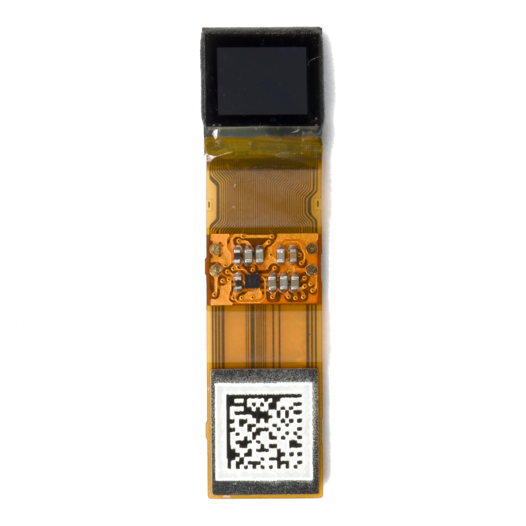
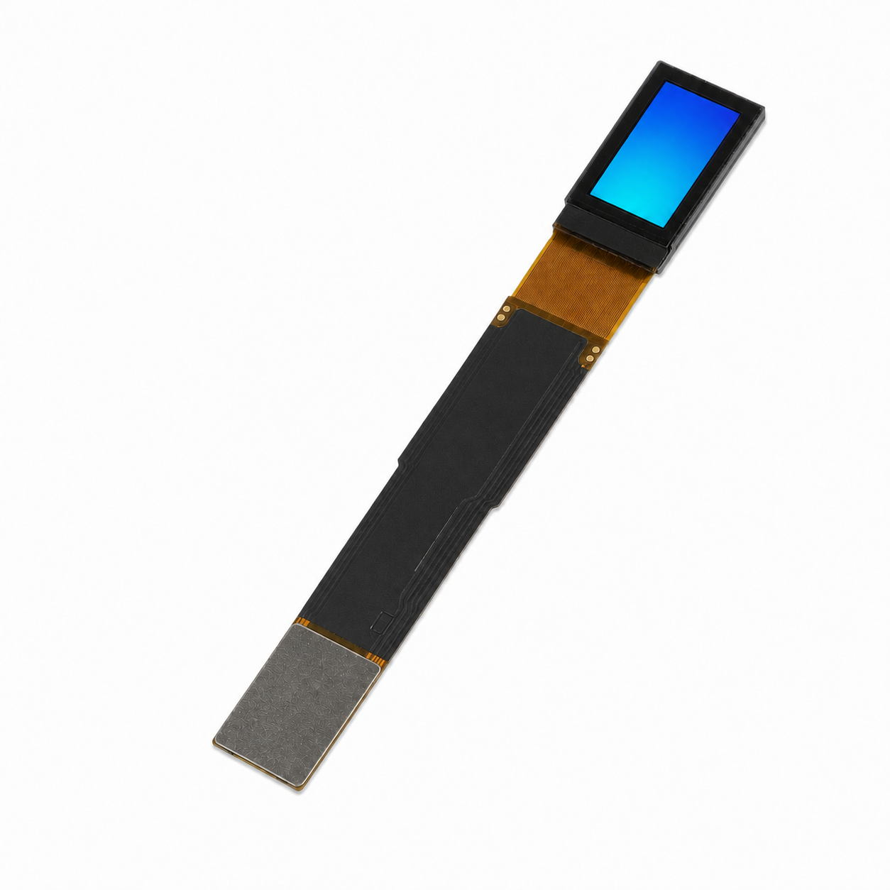
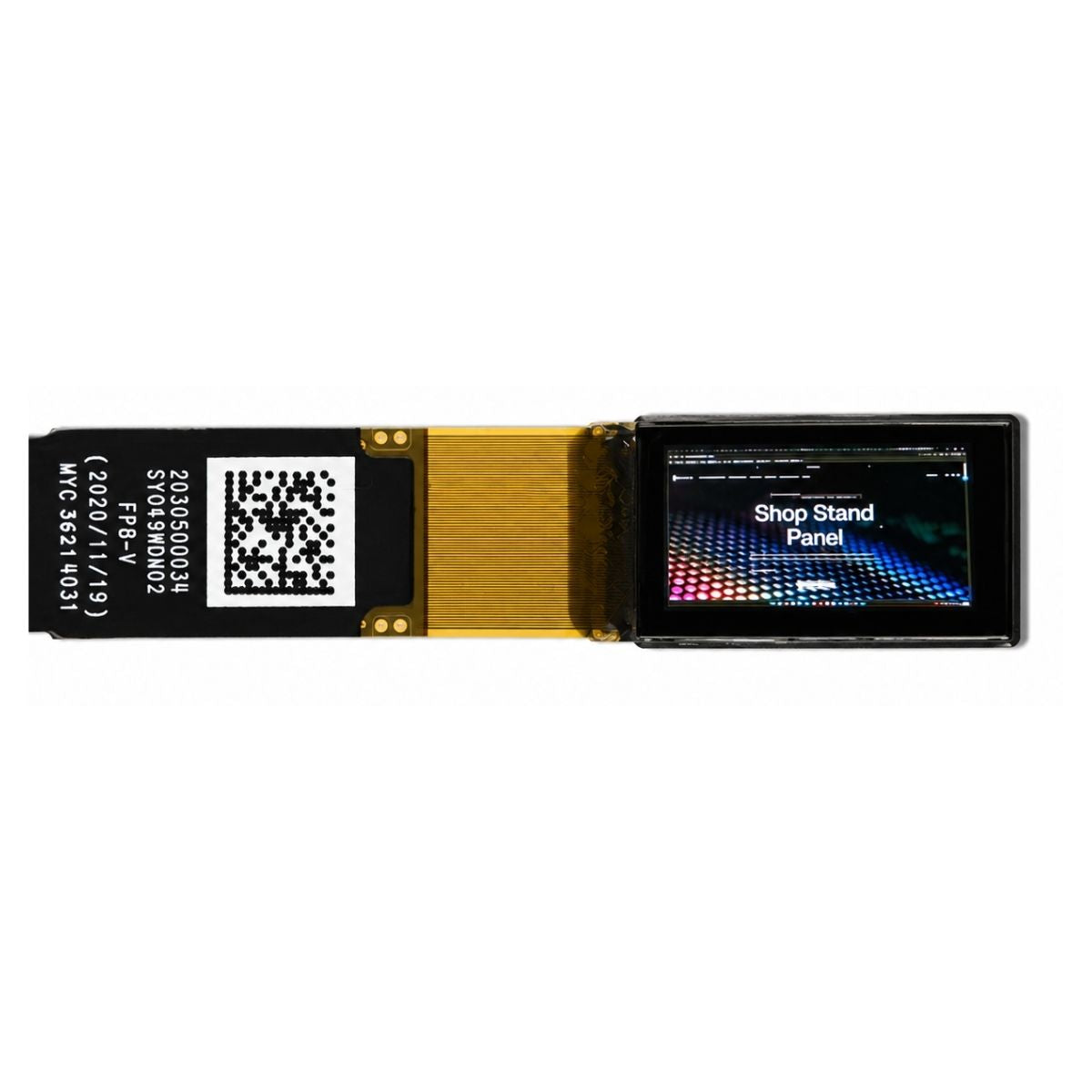
Do not decide the mode from the words “MIPI DSI” or from the lane count. Check the exact panel datasheet and initialization table. For example, this 4.82-inch 480 × 1120 MIPI DSI module is listed as video mode, while this 2.4-inch 450 × 600 AMOLED module supports command mode.
For a basic explanation of the interface, read What Is MIPI DSI?. For interface selection, see MIPI DSI vs RGB vs SPI vs LVDS.
What the TE Signal Does
TE means Tearing Effect. The display controller creates this signal at a known point in its refresh cycle. The host uses that point to decide when to start a command-mode update.
The common MIPI Display Command Set commands are:
| Command | Hex value | Purpose |
|---|---|---|
| Set Tearing Effect Line Off | 0x34 |
Disable the TE output |
| Set Tearing Effect Line On | 0x35 |
Enable the TE output |
| Set Tearing Effect Scan Line | 0x44 |
Select a scanline used as the TE trigger, when supported |
The parameter sent with 0x35 normally selects one of these modes:
- Vertical blanking information only
- Vertical and horizontal blanking information
Start with vertical-only mode unless the panel documentation says otherwise. It normally gives one main TE event per refresh. Vertical-and-horizontal mode can produce many events in one frame and is easier to handle incorrectly.
The expected period is the inverse of the refresh rate. These values are useful when checking the TE pin or interrupt counter:
| Refresh rate | Nominal TE period | Expected events in 10 seconds |
|---|---|---|
| 30 Hz | 33.33 ms | About 300 |
| 60 Hz | 16.67 ms | About 600 |
| 90 Hz | 11.11 ms | About 900 |
| 120 Hz | 8.33 ms | About 1,200 |
For example, a fixed 60 Hz panel should produce about 600 vertical-only TE events in 10 seconds. A count close to 1,200 often means that both edges are enabled. A much higher count points to horizontal events, noise, a floating pin, or an interrupt flag that is not being cleared.
TE is a timing marker, not a time window. Do not assume that data may be sent only while the pin is high. The useful point may be the rising edge, falling edge, start of a low pulse, end of a low pulse, or a selected scanline transition. Check the panel timing diagram and verify the result with a moving test pattern.
TE does not increase DSI bandwidth, lock the framebuffer, clean cache, or stop two transfers from overlapping. Firmware must still handle those jobs.
Check the Panel Documentation First
Before connecting or enabling TE, confirm the following items from the exact module and controller documents:
- Command mode, video mode, or a vendor-specific mixed mode
- Whether the panel has internal GRAM
- Whether TE works in the selected mode
- TE voltage, output type, polarity, pulse width, and active edge
- Supported
0x35values - Whether
0x44is supported - Physical scan direction and rotation behavior
- Power, reset, sleep-out, display-on, and TE command order
- Whether TE must be enabled again after sleep or reset
The exact module datasheet is more important than a generic controller example because module makers may change power rails, pull resistors, pin wiring, or initialization settings. The guide How to Read a TFT LCD Module Datasheet shows where to find pin, timing, and initialization information.
Check the TE Pin and Voltage
Do not connect TE to the host until the electrical levels are known. Check:
- Panel output-high and output-low limits
- Host GPIO input thresholds
- Host absolute maximum voltage
- TE state when the panel is unpowered
- Whether the panel and host can be powered separately
A 2.8 V TE output can damage a 1.8 V-only GPIO even when early tests appear to work. Use a suitable level translator when needed. If one side can be powered off separately, use a translator with power-off isolation so the active side does not feed current into the unpowered side.
The TE output may be push-pull, open-drain, open-collector, or register-controlled. An open-drain output needs a pull-up to a safe voltage. A push-pull output normally does not need a strong pull-up because it adds current when the output is low and may affect voltage margins or level shifting.
A typical connection is:
Panel TE output
      |
      +---- optional series resistor ---- host GPIO or TE input
      |
      +---- pull-up only if required by the panel output type
Configure the host pin as an input during reset and boot. Disable button-style debounce unless testing proves it is safe. A debounce or glitch filter can remove a short TE pulse.
Add a TE test point on prototype boards. Measure the voltage, pulse width, period, active edge, first pulse after initialization, and behavior after sleep and resume.
Use the Correct Initialization Order
The exact order is panel-specific, but a common sequence is:
Apply panel power
Assert reset
Release reset
Wait for controller startup
Send vendor initialization commands
Set pixel format and orientation
Exit sleep mode
Wait for the required delay
Enable TE
Turn the display on
Wait for a new TE event
Start normal updates
Some panels need TE enabled before Display On. Others do not drive TE until the display is already on. Reset, sleep-in, display-off, or power loss may clear the TE setting, so the resume path may need to send 0x35 again.
A basic DCS write may look like this:
uint8_t te_mode = 0x00; /* Example only; check the panel datasheet. */

int ret = dsi_dcs_write(0x35, &te_mode, 1);
if (ret < 0)
    report_panel_error(ret);
A successful function return normally means that the host accepted or sent the command. It does not prove that the panel is producing TE pulses. Measure the physical pin after initialization and after resume.
Prepare the Update Before TE Arrives
The display path should do most work before the TE event:
- Finish rendering the frame or changed region
- Choose and merge dirty rectangles
- Prepare the address commands
- Prepare DMA descriptors
- Clean the cache range used by DMA
- Choose the pending buffer
- Mark the update ready
When TE arrives, the fast path should only check that the event is new, check that no transfer is active, send the prepared commands, and start DMA.
Do not decode images, allocate memory, copy a full framebuffer, clean a large cache range, access storage, wait on a long mutex, or print slow debug logs after TE. These tasks use the timing margin before pixel transfer even starts.
Whether column, page, and memory-write commands may be sent before TE depends on the controller. Prepare the command bytes early, but send them at the point required by the panel manual.
Keep the TE Interrupt Short
The TE interrupt handler should clear the interrupt, record the event, and wake the display task. It should not render or wait for the transfer to finish.
static volatile uint32_t te_sequence;
static volatile uint32_t te_timestamp;

void TE_IRQHandler(void)
{
    clear_te_interrupt_flag();

    te_timestamp = read_free_running_timer();
    te_sequence++;

    notify_display_task_from_isr();
}
The task must read the sequence and timestamp as one consistent pair. On a single-core MCU, use a short critical section that blocks the TE interrupt while both values are copied:
struct te_event {
    uint32_t sequence;
    uint32_t timestamp;
};

static struct te_event read_te_event(void)
{
    struct te_event event;
    irq_state_t state = enter_te_critical_section();

    event.sequence = te_sequence;
    event.timestamp = te_timestamp;

    exit_te_critical_section(state);
    return event;
}
On a multi-core system, use a lock, a hardware capture register, or another method that guarantees a consistent pair. Two separate atomic variables are not enough unless the read and write method prevents a new timestamp from being paired with an old sequence number.
Do not queue every TE pulse. Use a notification plus a sequence counter. If the panel generates 60 events per second but the application produces 20 new frames per second, most TE events require no transfer.
Reject Old or Late TE Events
A task may wake from an old semaphore or event flag. It must compare the current TE sequence with the last sequence it used.
struct te_event event = read_te_event();

if (event.sequence == last_te_sequence)
    return; /* No new TE event. */

last_te_sequence = event.sequence;

uint32_t age = read_free_running_timer() - event.timestamp;
if (age > MAX_TE_START_LATENCY) {
    late_te_count++;
    return; /* Wait for the next TE event. */
}

if (!frame_ready || !dsi_transaction_ready())
    return;

start_prepared_update();
MAX_TE_START_LATENCY must come from measurements. A late transfer may reach the panel scan at the wrong time, so skipping one frame can be safer than starting too late.
At 60 Hz, one frame lasts 16.67 ms. Even a small delay can use a noticeable part of that period:
| TE-to-transfer delay | Share of a 60 Hz frame period |
|---|---|
| 0.5 ms | About 3% |
| 1 ms | About 6% |
| 2 ms | About 12% |
| 5 ms | About 30% |
This table does not define an acceptable delay. It only shows why image rendering, cache cleaning, and large memory copies should finish before TE.
Keep DMA Completion and Link Completion Separate
The following events may happen at different times:
- DMA stops reading the source buffer
- The DSI transmit FIFO becomes empty
- The long packet finishes
- The PHY reaches the required idle state
- An acknowledgement or bus-turnaround operation finishes
The source buffer may be reused after DMA has definitely stopped reading it. The next DSI transaction may still need to wait until the host reports a later link-ready event.
static bool source_dma_busy;
static bool dsi_link_busy;
static frame_t *dma_buffer;

void on_source_dma_complete(void)
{
    source_dma_busy = false;

    release_frame(dma_buffer);
    dma_buffer = NULL;
}

void on_dsi_link_complete(void)
{
    dsi_link_busy = false;
}

bool dsi_transaction_ready(void)
{
    return !source_dma_busy && !dsi_link_busy;
}
Use the completion flags defined by the host-controller manual. Do not clear one generic transfer_active flag at DMA completion unless the manual states that the DSI link is also ready at that point.
Protect the Source Buffer and Cache
TE does not stop the graphics library from changing the source buffer while DMA is reading it. That can send part of the old image and part of the new image even when the TE edge is correct.
Keep these states separate:
- Rendering complete: Drawing has finished.
- Source DMA complete: DMA no longer reads the buffer.
- DSI link complete: The host can start the next required transaction.
With double buffering, render into one buffer while the other buffer is pending or being sent. With triple buffering, one buffer can be sent, one can wait for TE, and one can be rendered.
For a low-latency GUI, keep only the newest completed frame that has not started transmitting. Do not build a long queue of old frames. Do not use this drop policy when every frame must be kept.
On a non-coherent cached processor, use this order:
Finish rendering
Clean the DMA-visible cache range
Run the required memory barrier
Mark the frame ready
Wait for a new TE event
Start DMA
Cache clean addresses and lengths often need cache-line alignment. When only a small area changes, clean that area before TE instead of cleaning the full framebuffer after TE.
Calculate the Real Timing Budget
Start with the amount of pixel data:
RGB565 bytes = width × height × 2
RGB888 bytes = width × height × 3
The table below shows the uncompressed size of one frame. RGB888 always carries 1.5 times as much pixel data as RGB565 at the same resolution.
| Resolution | Pixel count | RGB565 frame size | RGB888 frame size |
|---|---|---|---|
| 240 × 320 | 76,800 | 153,600 bytes | 230,400 bytes |
| 480 × 800 | 384,000 | 768,000 bytes | 1,152,000 bytes |
| 720 × 1280 | 921,600 | 1,843,200 bytes | 2,764,800 bytes |
| 1080 × 1920 | 2,073,600 | 4,147,200 bytes | 6,220,800 bytes |
A 480 × 800 RGB565 frame therefore contains:
480 × 800 × 2 = 768,000 bytes
768,000 × 8 = 6,144,000 bits
The nominal frame period changes with the refresh rate:
30 Hz  = 33.33 ms
60 Hz  = 16.67 ms
90 Hz  = 11.11 ms
120 Hz = 8.33 ms
Do not assume that the complete period is available for writing. The usable time depends on the TE position, scan direction, update area, active-scan rules, internal buffering, and refresh mode.
The full update time is:
Total update time =
TE-to-start delay
+ DCS command time
+ LP/HS switching time
+ pixel transfer time
+ FIFO and DMA gaps
+ required link completion time
Assume two active lanes at 500 Mbit/s per lane:
Raw lane rate = 2 × 500 Mbit/s = 1,000 Mbit/sAt that raw rate, the payload-only times for RGB565 are:
| Resolution | RGB565 payload | Payload-only time at 1 Gbit/s | Compared with a 60 Hz period |
|---|---|---|---|
| 240 × 320 | 1,228,800 bits | 1.229 ms | 7.4% |
| 480 × 800 | 6,144,000 bits | 6.144 ms | 36.9% |
| 720 × 1280 | 14,745,600 bits | 14.746 ms | 88.5% |
| 1080 × 1920 | 33,177,600 bits | 33.178 ms | 199.1% |
These are theoretical lower limits. They exclude packet headers, ECC, CRC, commands, mode changes, memory delays, FIFO stalls, and panel or host limits. The table shows why a 720 × 1280 full-frame update has little margin at this lane rate and why a 1080 × 1920 frame cannot fit inside one 60 Hz period even before protocol overhead is added.
If the 480 × 800 payload takes 9.6 ms in a real system, its effective payload rate is:
6,144,000 ÷ 0.0096 = 640 Mbit/sMeasure these points with a logic analyzer, oscilloscope, host timestamp, or spare GPIO marker:
T0 = TE edge
T1 = ISR entry
T2 = first DSI command
T3 = first pixel packet
T4 = source DMA complete
T5 = required DSI link completion
Record the minimum, maximum, and spread for each interval. For example:
TE start jitter = maximum TE-to-first-pixel delay
                - minimum TE-to-first-pixel delay
Use the worst result under normal product load, not the average result from an idle demo. Test CPU load, memory traffic, storage, networking, low-power wake-up, the largest update area, and every supported rotation.
If the update does not fit, increase the lane rate within panel limits, use more lanes, reduce color depth, send a smaller area, lower the update rate, reduce repeated LP/HS switches, or improve DMA and memory priority. TE cannot fix a transfer that is too slow.
Use Partial Updates Carefully
A partial update normally sends a column range, page range, memory-write command, and the pixels for that rectangle.
For inclusive coordinates from (x1, y1) to (x2, y2):
Width  = x2 - x1 + 1
Height = y2 - y1 + 1
Bytes  = width × height × bytes_per_pixel
A small update can still tear if it starts from the wrong TE edge, begins too late, overlaps the active scan, or reads a buffer that is still being changed.
For a 480 × 800 RGB565 screen and a 1 Gbit/s raw lane total, the data savings can be large:
| Update area | Pixel data | Share of full frame | Payload-only time |
|---|---|---|---|
| 100 × 100 | 20,000 bytes | 2.60% | 0.160 ms |
| 200 × 200 | 80,000 bytes | 10.42% | 0.640 ms |
| 480 × 80 | 76,800 bytes | 10.00% | 0.614 ms |
| 240 × 400 | 192,000 bytes | 25.00% | 1.536 ms |
| 480 × 800 | 768,000 bytes | 100.00% | 6.144 ms |
The times in this table cover pixel payload only. A very small rectangle may still be inefficient if each region repeats address commands, packet setup, and LP/HS switching.
Check these details:
- Even-pixel or byte-alignment rules
- Minimum update width
- Framebuffer stride
- Two-dimensional DMA support
- Panel rotation and memory-access-control settings
- Physical scan direction
A framebuffer may show 480 visible pixels per row but use a 512-pixel memory stride. In that case, a rectangle is not one continuous memory block. Configure row length and source stride, send one row at a time, or pack the area into a compact buffer.
Several small rectangles can be slower than one merged rectangle because each one repeats commands and LP/HS switching. Merge nearby areas when the extra pixels cost less than another transaction.
Use Scanline TE Only When Needed
The 0x44 command can select a scanline for TE when the controller supports it. This may help when the same screen area is updated repeatedly.
Do not assume that the scanline value equals the GUI Y coordinate. It may follow the panel’s native orientation, physical gate order, hidden timing lines, or a controller-specific range. Rotation may also change the meaning.
Start with normal vertical-only TE. Use scanline TE only after checking the accepted range, byte order, active edge, rotation behavior, and sleep/resume behavior. A wrong scanline can create a fixed tear line that looks like a bandwidth problem.
Add a Timeout and Recovery Path
Never wait forever for TE. The signal can stop after sleep, display-off, reset, power loss, cable failure, GPIO reconfiguration, refresh-rate change, or self-refresh entry.
Base the timeout on the slowest expected TE period:
TE timeout > maximum valid TE period + worst software delayA 60 Hz panel has a nominal 16.67 ms period, but 40 ms, 50 ms, or 100 ms is not a universal timeout. Low-refresh and variable-refresh modes can use longer periods.
After a timeout:
- Check whether the application is supposed to update the screen.
- Check panel power, reset, sleep, and display-on state.
- Check that the TE pin is still configured as an input.
- Clear old interrupt status and old task notifications.
- Re-enable the TE interrupt.
- Send the TE enable command again if required.
- Wait for a new TE sequence.
- Reinitialize the panel if TE does not return.
- Power-cycle the panel only after the lighter steps fail.
Clear pre-sleep TE events and old pending-frame state during reset or resume. Do not send an unsynchronized full frame automatically after every TE timeout.
If TE loss is part of a no-image problem, use MIPI DSI Black Screen Debugging to check power, reset, link activity, and the pixel source in order.
Linux Driver Notes
Current Linux panel drivers can use the multi-context helper:
struct mipi_dsi_multi_context ctx = {
    .dsi = dsi,
};

mipi_dsi_dcs_set_tear_on_multi(
    &ctx,
    MIPI_DSI_DCS_TEAR_MODE_VBLANK
);

if (ctx.accum_err)
    return ctx.accum_err;
Older drivers may use mipi_dsi_dcs_set_tear_on(), but current Linux documentation marks that helper as deprecated in favor of mipi_dsi_dcs_set_tear_on_multi().
These helpers enable the panel’s TE output. They do not automatically make every framebuffer update wait for TE. A command-mode driver may still need TE interrupt handling, update scheduling, damage rectangles, framebuffer fences, buffer lifetime control, transfer completion, and resume handling.
For a normal video-mode DRM pipeline, use vertical-blank and page-flip synchronization. Enabling the panel TE output does not replace the DRM scanout system.
Test the Complete Update Path
Use a moving, high-contrast pattern. A static logo cannot show whether two frames are mixed.
Useful patterns include a white bar moving over black, a one-pixel-moving checkerboard, alternating black and white frames, scrolling text, and a moving diagonal line.
Test in this order:
- TE only: Measure voltage, pulse width, period, edge, and interrupt count.
- Start delay: Mark ISR entry, first command, and first pixel packet.
- Region size: Test 50 × 50, 200 × 200, half screen, and full screen.
- Buffer ownership: First send an unchanged buffer, then allow normal rendering during transfer.
- Product load: Repeat with storage, networking, animation, power-state changes, and memory load.
| Symptom | Check first | Likely area |
|---|---|---|
| No TE pulse | TE pin waveform | Power, reset, command order, wiring, pull-up |
| Too many TE interrupts | Interrupt count and edge setting | V/H mode, both edges, uncleared flag, noise |
| Fixed tear line | Edge, scanline, and transfer time | Wrong edge, wrong scanline, scan direction, bandwidth |
| Moving tear line | TE-to-start delay | Scheduling, wake-up, DMA, memory contention |
| Small update works | Full-frame transfer time | Full update is too slow |
| Random blocks or wrong colors | Buffer, stride, cache, packet errors | Memory or DSI data path, not only TE timing |
| Failure after resume | TE waveform after wake | TE command or GPIO state was not restored |
| Old frames appear late | Pending-frame queue | Old frames or old TE events are being consumed |
Release Checklist
- The panel mode and TE behavior are confirmed from the exact datasheet.
- The TE voltage, output type, pull-up, and power-off behavior are safe.
- The active edge, pulse period, and interrupt count have been measured.
- Rendering, command setup, and cache work finish before TE.
- The firmware requires a new TE sequence and rejects late events.
- The source buffer is not changed while DMA reads it.
- Source-DMA completion and DSI-link completion are handled separately.
- Only one DSI transaction starts at a time.
- Full and partial transfers are measured under real product load.
- Stride, alignment, rotation, and physical scan direction are tested.
- Sleep, resume, timeout, reset, and power-cycle recovery are tested.
- A moving high-contrast pattern shows no tear in every supported mode.
Sources
- MIPI Alliance: MIPI Display Serial Interface
- MIPI Alliance: MIPI Display Command Set
- Linux Kernel Documentation: Kernel Mode Setting
- Linux Kernel Documentation: MIPI DSI Helper Functions
- Linux Source: MIPI DSI and DCS Command Definitions
Conclusion
For a tear-free command-mode update, prepare the frame before TE, use the verified edge, and keep the DMA source unchanged until reading ends. At 60 Hz, each refresh lasts 16.67 ms. A 480 × 800 RGB565 frame contains 768,000 bytes and needs at least 6.144 ms on two 500 Mbit/s lanes before protocol overhead. A 100 × 100 update contains only 20,000 bytes, or 2.6% of that frame. Measure the worst TE-to-first-pixel delay and complete transaction time under full product load. If the transfer does not fit, reduce the area, increase supported bandwidth, or lower the update rate.
Laisser un commentaire
Ce site est protégé par hCaptcha, et la Politique de confidentialité et les Conditions de service de hCaptcha s’appliquent.