60 Hz typical
The frame-rate range is 55–65 Hz. The typical frame contains 823 lines, including 800 active lines and 23 lines of vertical blanking.


Popular Products


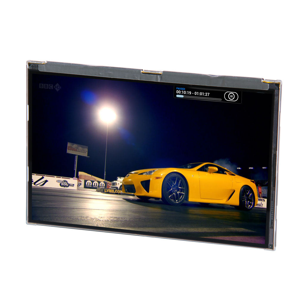
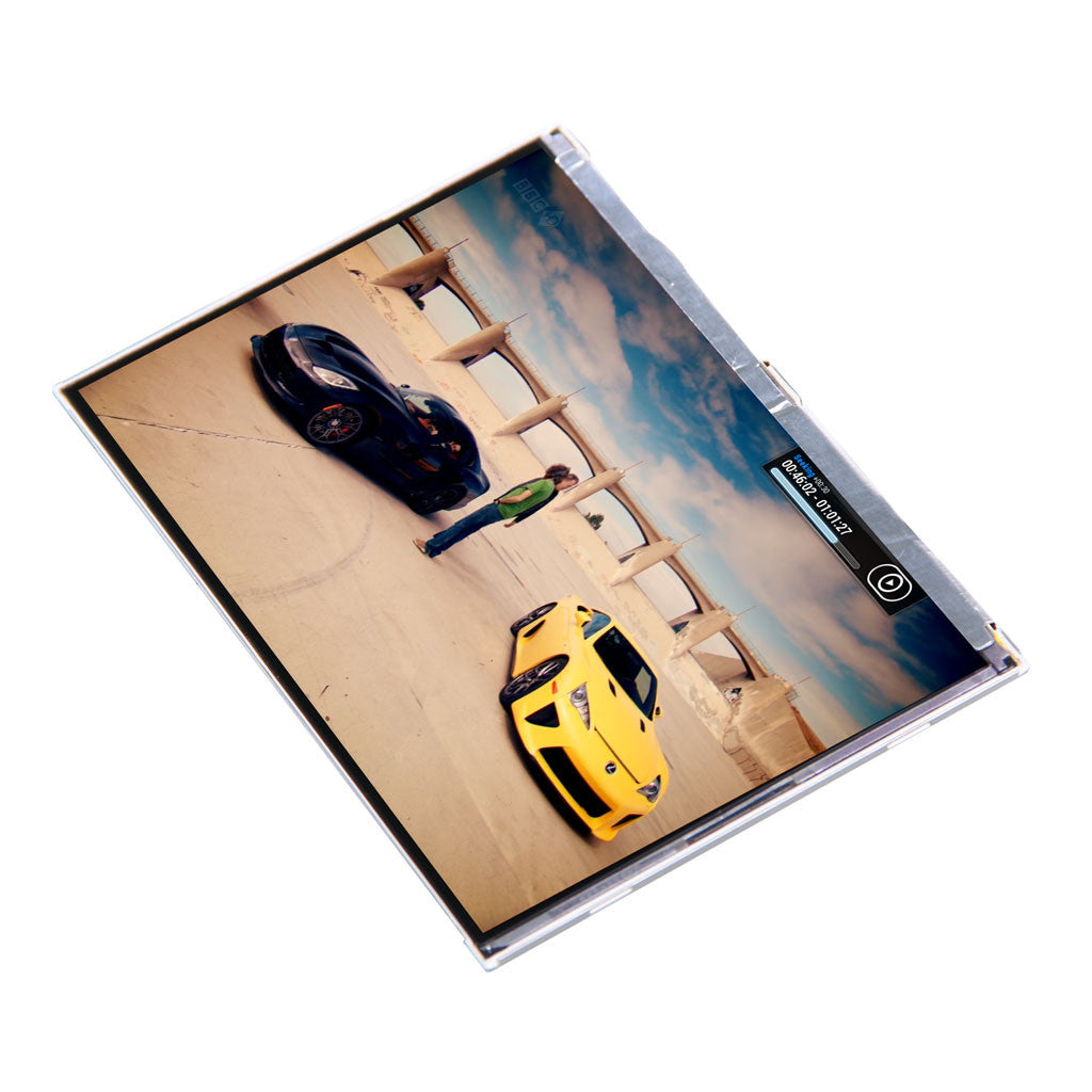
Interested in customizing this product? Get in touch with us.
Order samples, immediate delivery.
Factory bulk lead time: 3 weeks.
7.0" IPS Display 1280x800 - LVDS
DM-TFT70-301
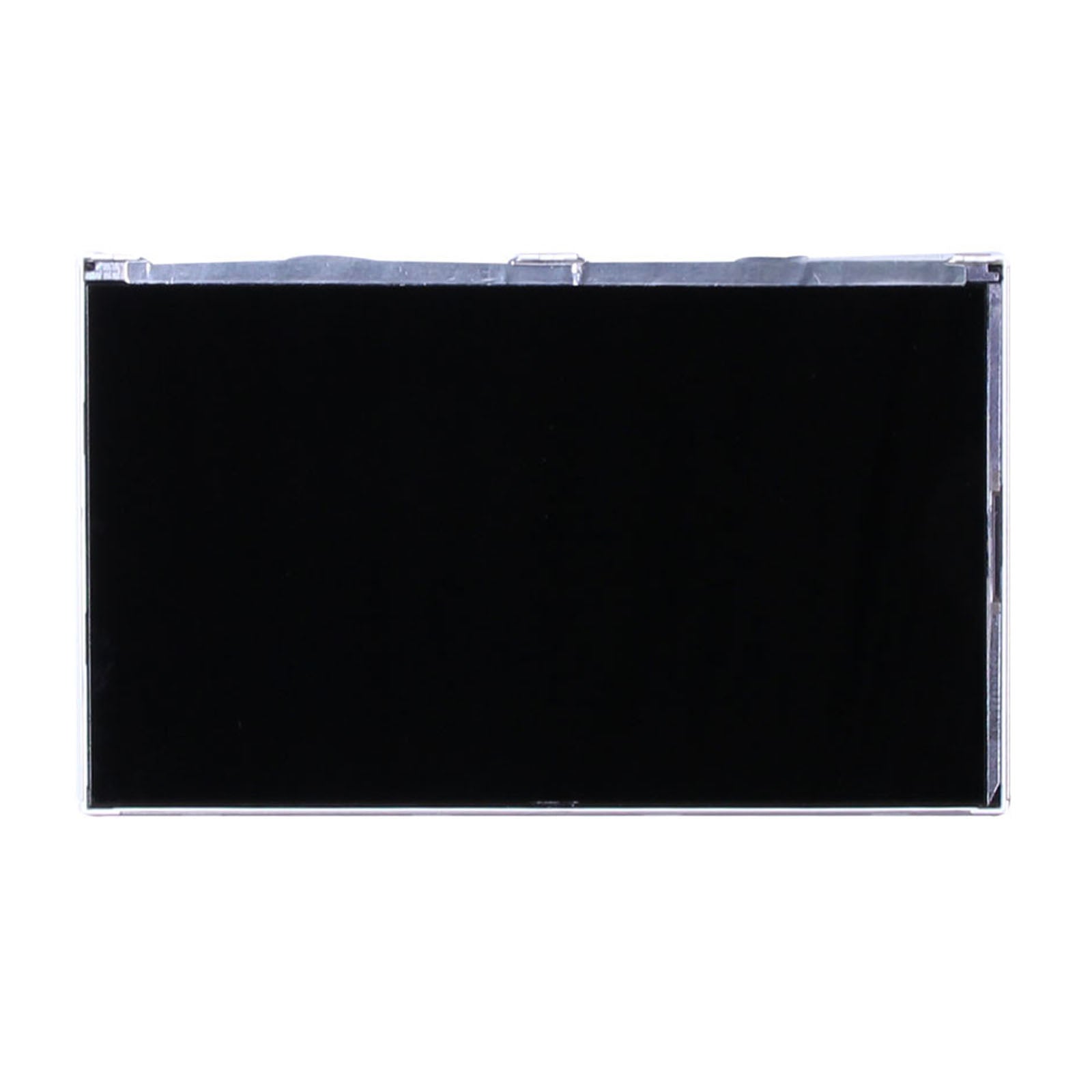
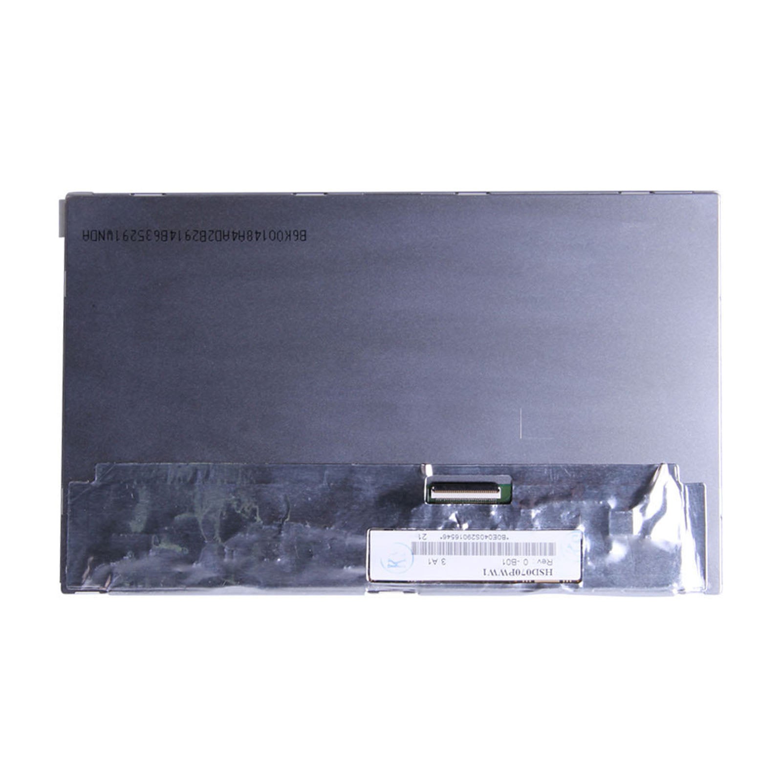
A 7-inch, 1280 × 800 display for information-rich landscape interfaces. DM-TFT70-301 pairs a 16:10 image area with single-channel LVDS and PWM brightness control, giving the host separate connections for image data and illumination.
Designed around the HSD070PWW1-B00 panel. Match the LVDS mapping, timing and supplied panel revision when choosing the controller and cable.
 + Click to enlarge
The HSD070PWW1-B00 panel accepts a single-channel LVDS signal with three differential data pairs and a differential clock pair. Its 6-bit red, green and blue inputs provide 262K colours across the 1280 × 800 matrix.
The LVDS pairs carry the pixel data and timing from the host to the panel receiver. A system using HDMI output requires a compatible display controller or conversion board. The panel connection includes separate power and ground pins alongside the differential signals.
The DE-mode timing specification includes active pixels and blanking intervals. These are the panel-side timing values used when configuring a compatible display output.
The frame-rate range is 55–65 Hz. The typical frame contains 823 lines, including 800 active lines and 23 lines of vertical blanking.
Clock rate is specified from 64.3 to 82 MHz. A typical line contains 1,440 clock periods, of which 1,280 carry active image data.
Typical horizontal blanking is 160 clocks. The timing specification also defines limits for line length and vertical blanking.
The values form a timing set; the minimum and maximum limits are not interchangeable presets. Frame rate depends on clock frequency and the complete horizontal and vertical periods.
DE-mode timing reference →| Parameter | Specification |
|---|---|
| Product model | DM-TFT70-301 |
| Display size | 7.0 inch |
| Resolution | 1280 × 800 pixels |
| Display connection | Single-channel LVDS |
| Controller / panel | HSD070PWW1-B00 panel |
| Display colours | 262K (6 bits per colour) |
| Touch configuration | No touch |
| Supply | 3.0–3.6 V; 3.3 V typical |
| Luminance | 320 cd/m² minimum; 400 cd/m² typical at IL = 20 mA |
| Mechanical reference | 161.2 × 105.5 mm typical; 4.2 mm typical / 4.5 mm maximum with PCB |
| Operating / storage temperature | −20 to +70 °C / −30 to +80 °C (absolute maximum ratings) |
The visible image, panel outline and PCB-inclusive depth describe different parts of the assembly.
Use the active area as the canvas for menus, charts and status regions. The 1280 × 800 matrix gives the software a 16:10 landscape format.
Size the panel pocket from the outside dimensions and their tolerances. The visible image area alone does not define the mounting envelope.
Depth is 4.2 mm typical and 4.5 mm maximum with the PCB. The module drawing and front-view CAD resource support the mechanical layout.
The 30-pin connector groups the image link into three differential data pairs and one differential clock pair. The pair assignment determines how the host’s RGB bits and control signals reach the panel.
The first data pair carries R0–R5 and G0. Pins 6 and 7 are the negative and positive inputs respectively.
RXIN1 on pins 9–10 carries G1–G5 and B0–B1. RXIN2 on pins 12–13 carries B2–B5 with HS, VS and DE.
The clock pair uses pin 15 negative and pin 16 positive. Ground positions separate the differential groups in the connector.
This mapping is useful when selecting an LVDS controller or preparing a cable: resolution alone does not specify the pin order, pair polarity or colour-bit assignment.
LVDS pin-assignment reference →The logic supply is 3.3 V typical, with a 3.0–3.6 V operating range. Pin 24, LED_EN, controls the backlight through PWM; pins 27–30 provide the separate LED power connection.
The specified PWM frequency is 18–22 kHz, with 20 kHz typical, and the dimming duty-cycle range is 20–100%. A higher duty cycle produces a brighter backlight. The host coordinates power, LVDS data and illumination using the panel’s power-on and power-off sequence.
The panel specification describes both its viewing surface and its optical transition time. These characteristics help distinguish the display itself from any cover lens added to the finished product.
The specified surface treatment includes anti-reflection of 1.5% or less and a 3H hard coating on a glare surface.
Combined rising and falling response time is 25 ms typical and 35 ms maximum under the optical measurement conditions.
The panel surface specification applies to the supplied panel. An added cover, adhesive layer or enclosure window introduces its own optical properties.
Response time describes the liquid-crystal transition, rather than touch latency or the host’s frame-rendering time. The panel datasheet provides the optical measurement definitions.
Optical-characteristics reference →Centre luminance is 320 cd/m² minimum and 400 cd/m² typical at IL = 20 mA. Contrast is 640:1 minimum and 800:1 typical. Viewing angles are 80° minimum and 89° typical in each direction at CR > 10.
These optical values apply under the specified measurement conditions, including a 25 ± 2 °C dark-room environment and 15-minute warm-up. The finished product’s cover, lighting and mounting position also affect the viewing result.
The controller must match single-channel LVDS with three data pairs, one clock pair and 6-bit RGB input. Check the 30-pin mapping, pair polarity and DE-mode timing as well as resolution. An HDMI source needs a suitable controller board.
LED_EN on pin 24 accepts PWM at 18–22 kHz, with 20 kHz typical and a specified 20–100% duty-cycle range. Increasing duty cycle increases brightness. Confirm the backlight supply and power sequence for the supplied panel revision before connecting VLED.
Yes. The mechanical table gives 4.2 mm typical and 4.5 mm maximum with the PCB; without the PCB it gives 2.35 mm typical and 2.65 mm maximum. Use the complete assembly envelope when sizing the enclosure.
Share the controller model, LVDS mapping and proposed cable pinout when requesting connection support for DM-TFT70-301. Include the PWM source and panel revision so that the backlight supply and sequencing can be confirmed.
For a sample or volume quote, specify the HSD070PWW1-B00 panel requirement and the available assembly depth. The linked HannStar document is Revision 1.0, marked tentative; confirm the supplied revision before freezing the mechanical or electrical design.
The HSD070PWW1-B00 reference covers LVDS mapping, optical conditions, mechanical limits and power sequencing. The separate DWG is a front-view CAD resource for the module.