


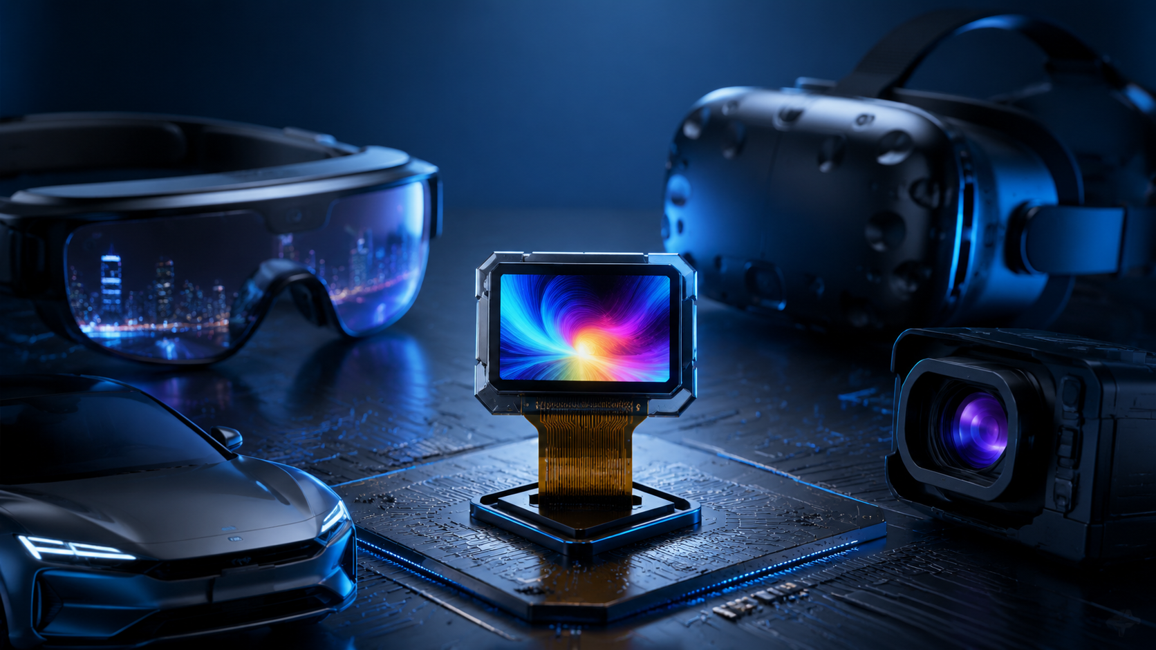
Custom Micro OLED Display Manufacturer for AR, VR, EVF and Near-Eye Devices
Micro OLED displays, also known as OLED-on-Silicon displays, combine high pixel density, fast response, high contrast, compact size, and efficient power performance under suitable drive conditions. These features make them suitable for AR glasses, VR headsets, electronic viewfinders, medical imaging systems, industrial inspection devices, and other near-eye display applications.
A typical high-end Micro OLED panel can exceed 3,000 PPI. For example, a 0.69-inch panel may support 2,560 x 1,920 resolution with peak brightness designed for near-eye optical engines. Actual brightness, optical efficiency, and perceived eye-box luminance depend on the optical architecture, display drive mode, thermal design, and end-device requirements.

Know the Display
Micro OLED Basics
Micro OLED, or OLED-on-Silicon, deposits organic light-emitting diode layers directly onto a CMOS silicon backplane rather than a glass substrate used in conventional AMOLED displays. The CMOS backplane integrates pixel-driving circuits beneath the emitting area, enabling extremely small pixel pitch, high fill factor, fast response, and compact module design.
Compared with conventional AMOLED, Micro OLED can achieve significantly higher pixel density because the silicon backplane supports finer circuit geometries. Compared with Micro LED, Micro OLED generally avoids mass-transfer challenges, although it still requires precise organic deposition, encapsulation, color management, and yield control.
A typical Micro OLED stack includes an anode, hole injection layer, hole transport layer, emissive layer, electron transport layer, electron injection layer, and cathode. The complete organic stack is usually very thin, often at micrometer scale. Material selection, deposition uniformity, encapsulation performance, and backplane design directly affect brightness, color gamut, lifetime, response time, and reliability.
| Layer / Process | Typical Material or Process | Key Engineering Consideration |
|---|---|---|
| Substrate | 8-inch or 12-inch CMOS wafer | Pixel circuit design, process node, wafer yield, and backplane uniformity |
| Anode | Reflective metal electrode | Reflectivity, surface roughness, and compatibility with organic deposition |
| Organic Stack | OLED emission and transport layers | Emission efficiency, color performance, lifetime, and deposition uniformity |
| Encapsulation | Thin-Film Encapsulation or Glass-Frit sealing | Moisture resistance, oxygen barrier performance, and long-term reliability |
| Module Assembly | Driver interface, FPC, bonding, and cover glass | Electrical stability, mechanical reliability, thermal path, and optical alignment |
- Organic deposition uniformity and chamber cleanliness are critical to brightness and color consistency.
- Encapsulation performance should be verified through humidity, temperature, and lifetime testing.
- Production yield should be reviewed by process stage, including wafer inspection, OLED deposition, encapsulation, bonding, and final module test.
Key Display Specifications
Evaluating Micro OLED display performance usually focuses on resolution, pixel density, brightness, contrast ratio, color gamut, color accuracy, refresh rate, response time, lifetime, interface, and power consumption. For near-eye systems, these parameters must be evaluated together with the optical engine rather than as isolated panel specifications.
Resolution defines the total number of physical pixels. Common Micro OLED resolutions include Full HD, 2.5K-class, and square-format panels for binocular optical engines. PPI is calculated from resolution and diagonal size. Higher PPI helps reduce visible pixel structure and supports higher perceived image sharpness in near-eye applications.
Contrast ratio is one of the major advantages of Micro OLED. Since OLED pixels are self-emissive, dark-state performance can be much better than LCD-based solutions. Fast pixel response also helps reduce motion blur, especially in VR and other motion-sensitive applications.
| Parameter | Typical Micro OLED Range | AR Design Focus | VR Design Focus |
|---|---|---|---|
| Resolution | 1920 x 1080, 2560 x 1920, 2560 x 2560 or higher | High pixel density for compact optical engines | High resolution for wide FOV and immersive images |
| Pixel Density | 2,000-5,000+ PPI | Usually above 3,000 PPI | Usually above 1,500 PPI |
| Brightness | 1,000-10,000+ cd/m², depending on model and drive mode | High panel brightness to compensate for optical loss | Balanced brightness, power, thermal design, and persistence |
| Contrast Ratio | High native contrast due to self-emissive pixels | Improves virtual image visibility and dark-state purity | Improves immersion and black-level performance |
| Color Gamut | Typically specified by sRGB, DCI-P3, or Rec.2020 coverage | High color accuracy for virtual-real image matching | Wide color gamut and consistent lens-corrected output |
| Response Time | Typically sub-millisecond to millisecond level | Reduces virtual-real motion mismatch | Reduces motion blur and supports low-persistence modes |
Near-Eye Display Fit
Near-eye displays are evaluated differently from conventional direct-view displays. Instead of screen size alone, system designers must consider field of view, eye-box size, pixels per degree, inter-pupillary distance, optical efficiency, distortion, eye relief, and user comfort.
Field of View, or FOV, describes the angular extent of the visible image. AR glasses often target compact FOV values for lightweight optical design, while VR headsets usually require much wider FOV for immersion. Pixels Per Degree, or PPD, is a key perceived-sharpness metric in near-eye systems.
Standard simplified PPD formula: PPD = horizontal pixel count / horizontal FOV in degrees. For example, a 2,560-pixel-wide display at 40° horizontal FOV provides about 64 PPD. The same display at 50° horizontal FOV provides about 51 PPD. In real optical systems, effective PPD may vary due to lens distortion, image cropping, pre-distortion rendering, optical alignment, and usable eye-box area.
Inter-Pupillary Distance, or IPD, is the distance between the centers of the user's pupils. Consumer near-eye devices must support appropriate IPD adjustment or optical tolerance to reduce eye strain, parallax error, and image discomfort. For AR and VR products, IPD design should be evaluated together with eye-box size, lens design, and binocular alignment.
Micro OLED panels can be integrated into systems that use techniques such as foveated rendering, eye-tracking synchronization, and low-persistence driving. These capabilities require close cooperation among the display supplier, optical module designer, driver IC team, algorithm team, and end-device manufacturer.
Choose the Manufacturer
Factory Capability Verification
The first step in selecting a Micro OLED manufacturer is to verify real production capability. Buyers should distinguish between display manufacturers, module integrators, trading companies, and agents. A qualified supplier should be able to provide clear information about wafer sourcing, OLED deposition, encapsulation, bonding, module assembly, inspection, reliability testing, and quality control.
On-site or remote factory audits should cover incoming wafer inspection, CMOS backplane testing, OLED deposition, encapsulation, FPC bonding, optical inspection, burn-in testing, and outgoing quality control. For mass production projects, buyers should review both sample performance and production yield history.
- Confirm whether the supplier owns or controls key OLED deposition, encapsulation, bonding, and test processes.
- Review process flow, equipment list, production capacity, and bottleneck processes.
- Request stage-by-stage yield data, including wafer test yield, deposition yield, encapsulation yield, bonding yield, and final test yield.
- Check inspection capabilities for brightness, chromaticity, mura, dark-state leakage, uniformity, response time, and lifetime.
- Verify burn-in conditions, defect classification rules, sampling plans, and outgoing quality criteria.
Custom Design Support
Custom Micro OLED design support reflects the manufacturer's engineering depth. Standard panels may be sufficient for evaluation or low-volume applications, but customized AR, VR, EVF, medical, or industrial devices often require panel, interface, optical, mechanical, and firmware-level support.
During specification review, the supplier should confirm resolution, active area, brightness, refresh rate, interface, power rails, timing, gamma, color calibration, thermal requirements, mechanical outline, and reliability targets. For custom designs, timing analysis and interface validation should confirm that pixel clock, MIPI bandwidth, setup and hold margins, and power sequencing are within safe operating limits.
Optical collaboration is especially important for near-eye devices. The display must be evaluated together with the optical module, such as prism, birdbath, pancake lens, waveguide, or EVF optics. Ray-tracing analysis, eye-box measurement, distortion correction, color uniformity, and luminance distribution should be reviewed at the system level.
- Interface options may include MIPI DSI, LVDS, parallel RGB, or customized driver interfaces.
- Brightness control may include DC dimming, PWM dimming, or hybrid dimming depending on flicker and power requirements.
- Color management may include gamma correction, white-point calibration, 3D LUT support, and Delta E control.
- Thermal design should consider panel brightness, duty cycle, enclosure material, heat spreading, and skin-temperature limits.
- Eye-tracking systems may require frame synchronization, low optical crosstalk, and reduced IR interference.
Quality Test Process
Micro OLED quality verification should follow a tiered test process from component-level inspection to module-level validation and system-level verification. A complete quality plan should define test conditions, instruments, sampling rules, pass/fail criteria, defect grading, and traceability.
Photoelectric tests usually include brightness, chromaticity, contrast ratio, color gamut, grayscale performance, gamma, mura, brightness uniformity, color uniformity, dark-state leakage, image retention, response time, viewing-angle performance, and power consumption. These tests should be performed under controlled ambient conditions using calibrated optical instruments.
Reliability tests usually include high-temperature operation, low-temperature operation, high-temperature high-humidity storage or operation, thermal shock, mechanical vibration, drop or shock testing, ESD, solder heat resistance, and lifetime evaluation. Test severity should be defined according to the target application and customer reliability requirements.
| Test Item | Typical Test Condition | Typical Pass Criterion |
|---|---|---|
| Brightness and chromaticity | Measured at defined grayscale, refresh rate, and drive mode | Within customer-approved specification limits |
| Mura inspection | White, gray, and dark-field images under controlled dark-room conditions | Meets agreed defect grade, such as A/B grade acceptance |
| Brightness uniformity | Multi-point measurement across the active area | Typically specified by minimum-to-maximum or standard-deviation method |
| Image retention | Static image stress followed by recovery measurement | Residual image level within agreed limit after defined recovery time |
| Color difference | Measured against target white point and color calibration standard | Delta E target defined by application, often tighter for AR and medical devices |
| High-temperature / high-humidity | Application-specific temperature, humidity, and duration | Brightness decay, color shift, and functional performance within limits |
| Thermal shock | Repeated cycling between low and high temperature | No package cracking, abnormal display, or electrical failure |
Build for Devices
AR Display Requirements
AR glasses place different requirements on Micro OLED displays than VR headsets. AR systems must overlay digital images onto the real world, so display brightness, optical efficiency, contrast, color accuracy, uniformity, and eye-box performance are critical. The required panel brightness depends on ambient light, optical path loss, lens or waveguide efficiency, target eye-box luminance, power budget, and thermal design.
Birdbath, prism, and waveguide optical systems can introduce significant optical loss. Therefore, AR-oriented Micro OLED panels often require higher peak brightness than VR-oriented panels. However, brightness should not be evaluated alone. A higher-brightness panel also increases power consumption, heat generation, lifetime stress, and optical design complexity.
- Brightness: selected according to optical efficiency, ambient light target, and eye-box luminance requirement.
- Uniformity: typically stricter than VR because edge vignetting is more visible in see-through AR systems.
- Response time: fast response helps reduce virtual-real motion mismatch.
- Color accuracy: important for matching virtual objects with real-world perception.
- IR compatibility: eye-tracking systems may require low IR crosstalk and stable frame synchronization.
- Thermal design: high-brightness AR panels require careful heat spreading and power management.
VR Display Requirements
VR headsets prioritize immersion, refresh rate, latency, resolution, persistence, and motion clarity. Since the display is magnified by lenses at near-eye distance, pixel structure, image blur, color fringing, distortion, and latency are more noticeable to users.
Motion-to-photon latency is a key comfort indicator. It represents the delay between user head movement and the corresponding image update. Display response time, refresh rate, rendering pipeline, sensor latency, and software optimization all contribute to the final latency.
Micro OLED's fast response can support low-persistence display modes, which reduce perceived motion blur. However, low-persistence driving may reduce effective brightness, so the display, driver IC, and optical engine must be optimized together.
- Refresh rate: usually 90 Hz or higher for comfortable VR applications.
- Low persistence: programmable emission duty can help reduce motion smear.
- Latency: display performance must be evaluated together with sensor, rendering, and system pipeline latency.
- Distortion correction: lens distortion and chromatic aberration should be corrected through optical design and rendering algorithms.
- Color consistency: panel calibration should reduce center-to-edge color and brightness variation.
- Eye-tracking compatibility: frame sync signal stability is important for foveated rendering and gaze tracking.
From Prototype to Mass Production
The standard new product introduction flow for Micro OLED projects is EVT, DVT, PVT, and then mass production. Each stage has a different purpose and should not be skipped for high-reliability AR, VR, EVF, medical, or industrial applications.
EVT: Engineering Validation Test
EVT verifies engineering feasibility. At this stage, the project team confirms whether the display architecture, interface, driver, optical path, thermal design, and mechanical integration can meet the main product requirements. EVT samples may still require design changes.
DVT: Design Validation Test
DVT validates the final or near-final design against the approved specification. The display is tested inside the actual optical module or device prototype. Key items include brightness, eye-box luminance, uniformity, color accuracy, distortion, thermal behavior, response time, power consumption, and reliability.
PVT: Production Validation Test
PVT confirms that the product can be manufactured repeatedly with stable process control, acceptable yield, traceability, and outgoing quality. Pilot production data should be reviewed before moving to full mass production.
| NPI Stage | Main Purpose | Key Output |
|---|---|---|
| EVT | Verify engineering feasibility | Engineering samples, risk list, design improvement plan |
| DVT | Validate final design performance | Validated specification, optical test report, reliability test report |
| PVT | Validate production readiness | Pilot run report, yield data, quality control plan, production release approval |
| MP | Mass production | Stable supply, traceable production lots, outgoing quality records |
During production ramp-up, manufacturers should track bonding yield, OLED deposition yield, encapsulation yield, final test yield, burn-in failure rate, and customer return data. A qualified Micro OLED supplier should provide DFM support, process risk review, reliability data, and clear change-control procedures.
Recommended NPI flow: EVT → DVT → PVT → MP. Working with a manufacturer that provides DFM review, optical validation, reliability qualification, and yield improvement support can reduce productization risk and shorten the time from prototype to stable production.
Summary
Selecting a Micro OLED display manufacturer requires more than comparing resolution and brightness. Professional buyers should evaluate the supplier's CMOS backplane capability, OLED deposition process, encapsulation quality, optical test capability, reliability validation, customization support, and mass-production yield control.
For AR, VR, EVF, and other near-eye devices, the best display solution is not simply the panel with the highest brightness or resolution. The right Micro OLED display should match the optical engine, product form factor, thermal design, interface, color target, lifetime requirement, and production schedule.
Read more
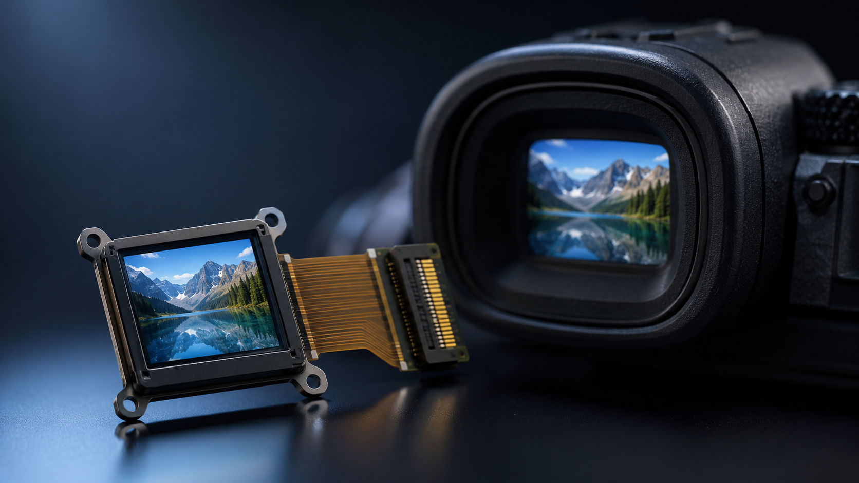
EVF viewfinders demand a display that can combine high pixel density, fast response, low latency, and a compact optical form factor. Among currently commercialized near-eye display technologies, Mi...
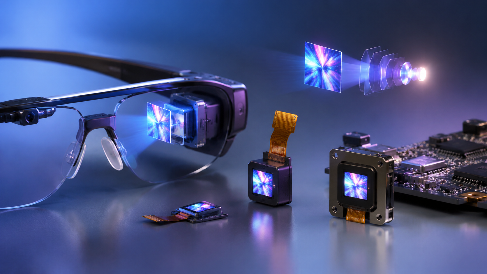
Micro OLED, also known as OLED-on-silicon or OLEDoS, is widely used in compact AR and VR optical engines because it combines self-emissive contrast, high pixel density and a small active display ...
Leave a comment
This site is protected by hCaptcha and the hCaptcha Privacy Policy and Terms of Service apply.