


PMOLED Advantages | Simplicity, Cost-Effectiveness & Performance
The advantage of PMOLED is what it leaves out. Removing the transistor backplane removes most of the process cost, most of the design effort and most of the standby current, and it lets a small monochrome module run from a plain SPI or I2C bus. The trade is scale: resolution, size and full-screen brightness all stay modest by design.
What the passive matrix removes
A PMOLED pixel is the area where an anode strip crosses a cathode strip. Nothing else sits in the pixel: no switch, no capacitor, no local memory. Selection is done entirely by the driver, which pulls one cathode row low and sources current into the anodes for that row.
That is also the constraint. Because the pixel holds no charge, it emits only during its own row time. The frame is a sequence of short pulses rather than a steady image, and the driver has to compensate by driving each pulse harder.
The compensating benefit is structural. Without a backplane there is no transistor variation to correct, no threshold drift to track, and no compensation circuit in the driver IC. The panel is a passive grid, and the electronics that would have gone into uniformity correction go into nothing at all.
Process and cost
Cost follows mask count. A passive backplane needs patterned ITO for the anodes, an insulating layer that defines the emitting openings, and cathode separators—inverted trapezoid structures that break the metal during evaporation and form isolated cathode strips without an extra etch step.
An active backplane needs a semiconductor layer with enough mobility to drive current, plus doping, gate insulator, interlayer dielectric, source and drain metal and a planarisation layer. Each added mask brings cleaning, deposition, coating, exposure, development, etch, strip and inspection, and each step carries a yield cost.
The difference is visible in tooling as well as unit price. A passive line does not need the laser anneal, the ion implanter or the stepper alignment budget that an LTPS line does, and the cycle time from glass to module is measured in days rather than weeks. For low and mid volumes that changes the economics of a custom shape or a custom icon layout, because the mask set is smaller and cheaper to commit to.

Stack and assembly
The emitting stack is thin—an anode, a hole transport layer, the emissive layer, an electron transport layer and a low work function cathode, all together well under a micron. What determines module thickness is the glass, the encapsulation and the polariser or antireflection film on the front.
Encapsulation is the part that decides field life. Moisture and oxygen attack the cathode and the emissive layer at the edges first, so thin film encapsulation or a desiccant-filled cavity is not optional. Ask for the specified storage and operating humidity range, not just the operating temperature.
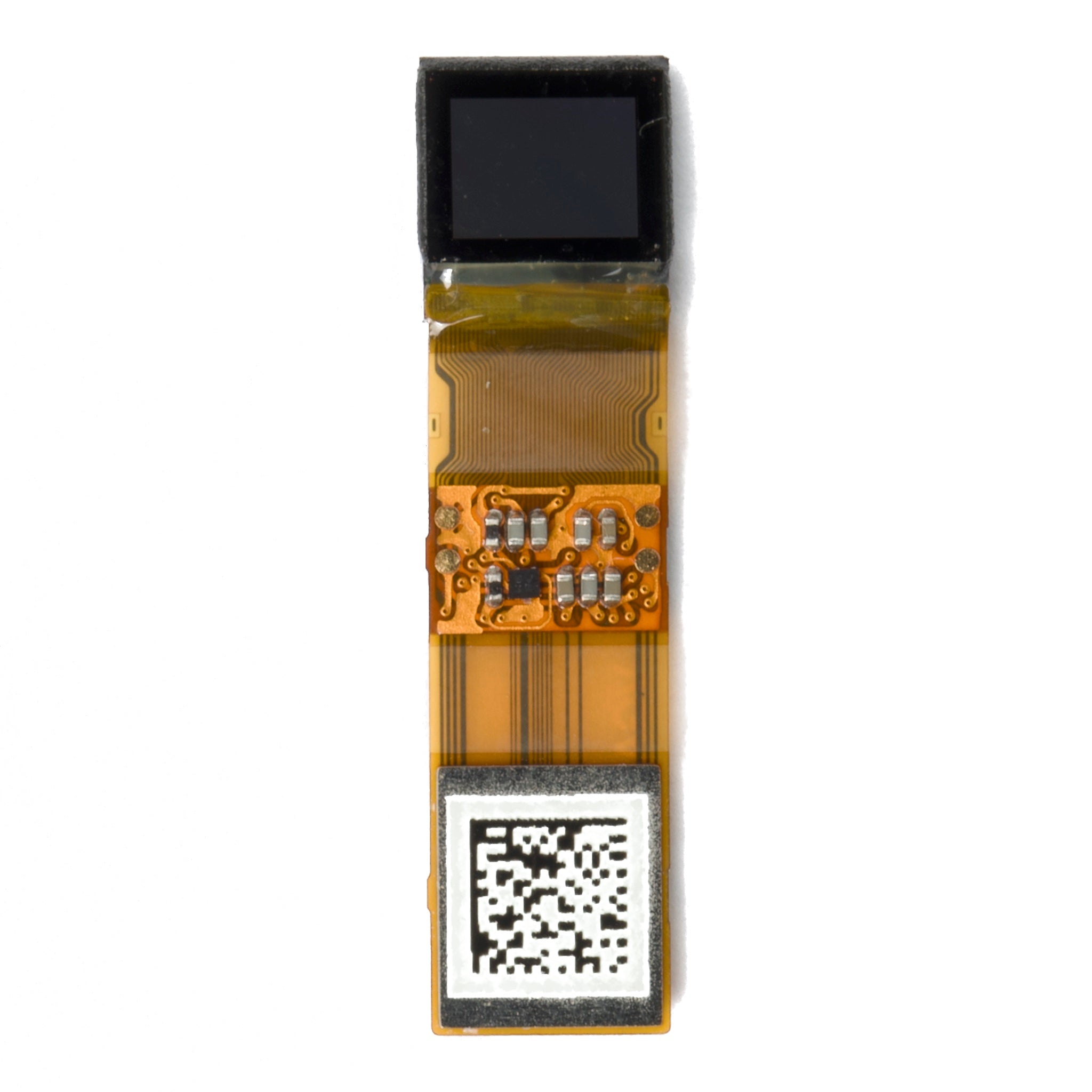
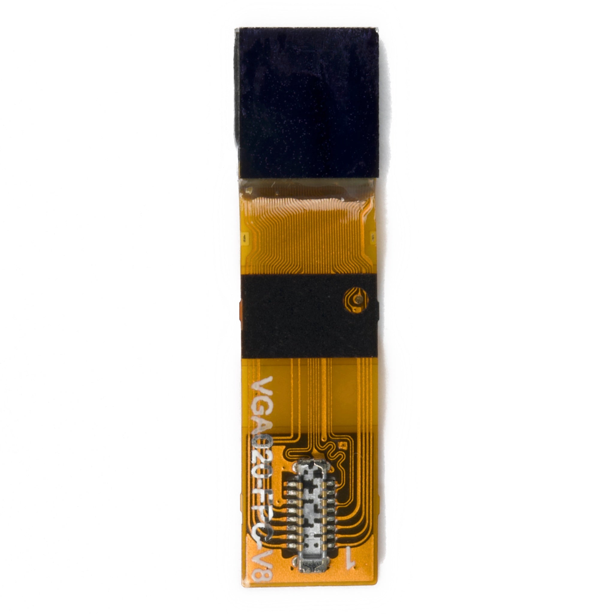
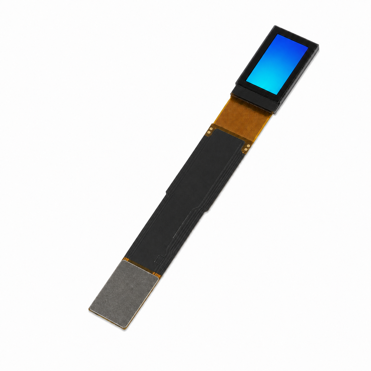
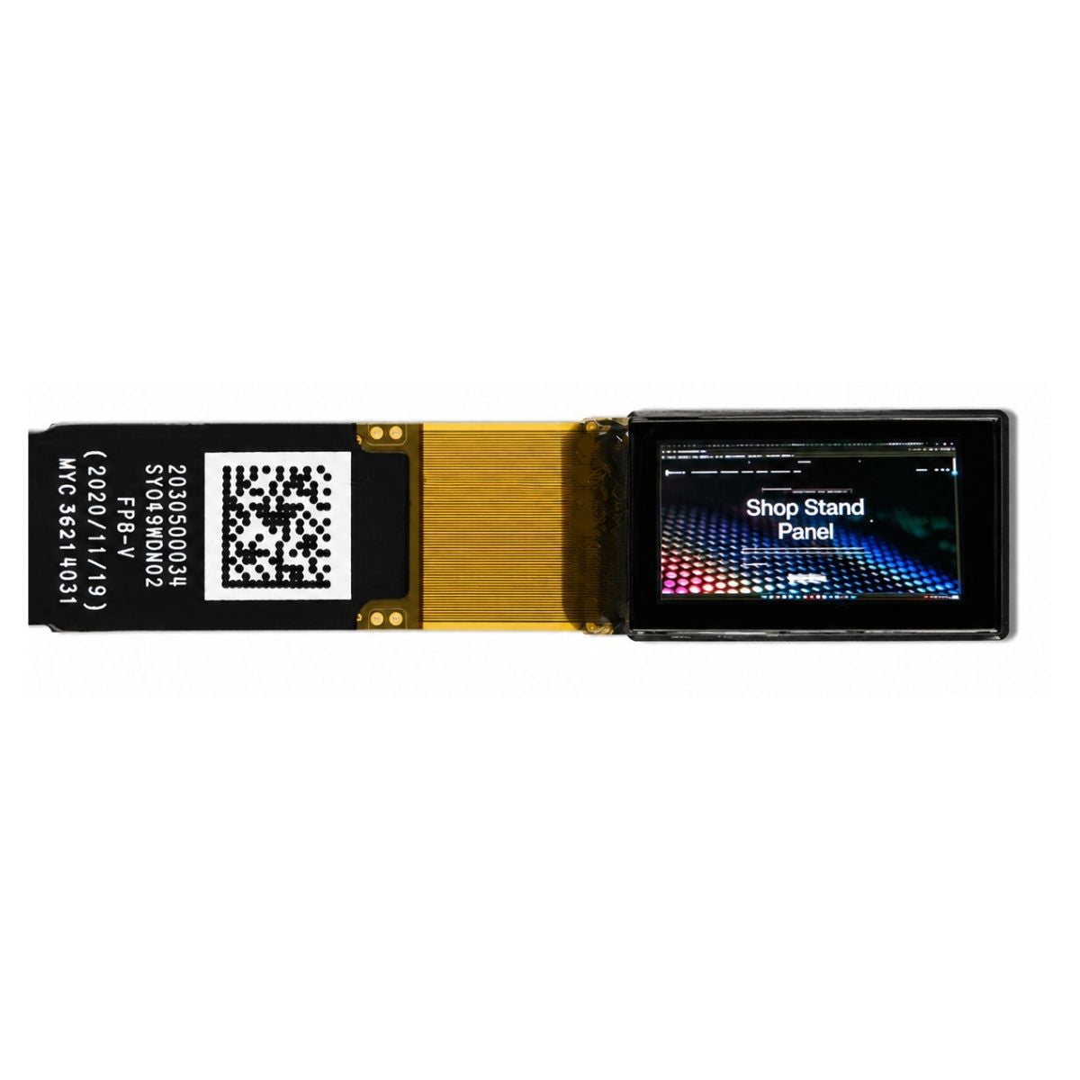
Assembly is where the passive structure pays off again. The driver is bonded directly to the glass—chip on glass—or to the flex tail, and the module needs no separate gate driver, because there are no gates to drive. That is why a passive module can be a few millimetres thick with a flex tail narrower than the panel.
Interface and firmware
From the host side the device looks like a small RAM. The driver holds a graphic RAM matching the panel resolution, and the microcontroller writes bytes into it over SPI or I2C; the driver handles multiplexing, row timing and brightness from there.
This is a real engineering saving. A passive module can be brought up with a handful of commands—set multiplex ratio to match the row count, set contrast, define the memory addressing mode, then stream the frame buffer. There is no timing controller to configure, no LVDS training, and no power sequence beyond supply and reset.
SPI capability is worth checking against the frame rate you need. Throughput depends on the clock, the bits per pixel and the overhead per transaction, so a 128×64 monochrome panel at a modest refresh is comfortable on a few megahertz, while a larger few-colour panel at video rate is not. I2C is slower again and shares the bus with sensors; size the bus before committing to an animation.
Performance limits
Three numbers describe the ceiling: duty cycle, peak luminance and lifetime. Duty cycle is set by the row count, peak luminance is what the driver and the emitter can deliver in that short window, and lifetime falls as peak luminance rises.
Contrast is a strength rather than a limit. An unlit OLED pixel emits nothing, so the dark state is limited by reflection from the front surface and the polariser, not by a backlight leaking through a liquid crystal layer. In a dim room the image reads as near-black between characters, which is why these modules suit instrument faces. Quoted contrast figures depend on the ambient light and the meter position, so compare them under the same conditions.[2]
Viewing angle is wide and symmetric because the emitter is Lambertian and the pixel has no cell gap or retardation to vary with angle. Colour shift with angle is small at the angles a handheld device is used, and greyscale inversion of the kind a twisted nematic cell shows does not arise.[1]
Response is fast enough to be treated as instantaneous for display purposes, since it is set by carrier recombination rather than by molecular rotation. That matters for a scrolling menu or a pointer, and it removes a whole class of design questions.
Temperature and lifetime
OLED ageing is driven by charge, so the same average brightness reached by higher peaks ages the material faster. Keeping brightness modest and content mostly dark is the most effective life extension available, and it costs no hardware.
Heat compounds it. Elevated temperature raises the rate of dark spot growth and accelerates the drop in efficiency, so a passive module inside a sealed enclosure needs its thermal path considered with the same seriousness as its current budget.
Burn-in follows the content, not the technology. A fixed frame held for hours will leave a ghost, so use a screen saver, shift the image by a pixel periodically, dim after inactivity, and avoid leaving a static test pattern during development.
Where PMOLED fits
It fits where the display is small, the information is sparse, and the budget is tight: wearable bands, handheld meters, medical readers, audio equipment, appliance panels, encryption tokens. It also fits where the mechanical envelope is thin and the flex must be narrow.
It does not fit a photographic viewer, a large control panel, or any product that needs a bright full-screen image in daylight. Those move to an active matrix or to a transmissive LCD with a strong backlight.
Standard parts, including character and graphic versions with chip-on-glass drivers, are listed under PMOLED displays, character OLED modules and graphic OLED displays.
Simplicity is the product: fewer masks, fewer components, fewer configuration registers. Specify the row count, the peak brightness at that duty cycle and the lifetime at the brightness you will actually use, and the rest of the module follows.
References
- Hilsum, C. (2010). Flat-panel electronic displays: a triumph of physics, chemistry and engineering. Philosophical Transactions of the Royal Society A, 368(1914), 1027–1082. https://doi.org/10.1098/rsta.2009.0247
- ISO 9241-307:2008 — Ergonomics of human-system interaction — Part 307: Analysis and compliance test methods for electronic visual displays. International Organization for Standardization. https://www.iso.org/standard/40102.html
Read more
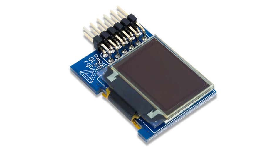
It is recommended to purchase modules under 3 inches with a resolution of 128×64. Use 4-pin I2C when I/O is limited, and select SPI for high-speed.

Manufacturing requires the use of vacuum thermal evaporation technology to deposit an organic material layer with a total thickness of approximately 150.
Leave a comment
This site is protected by hCaptcha and the hCaptcha Privacy Policy and Terms of Service apply.