

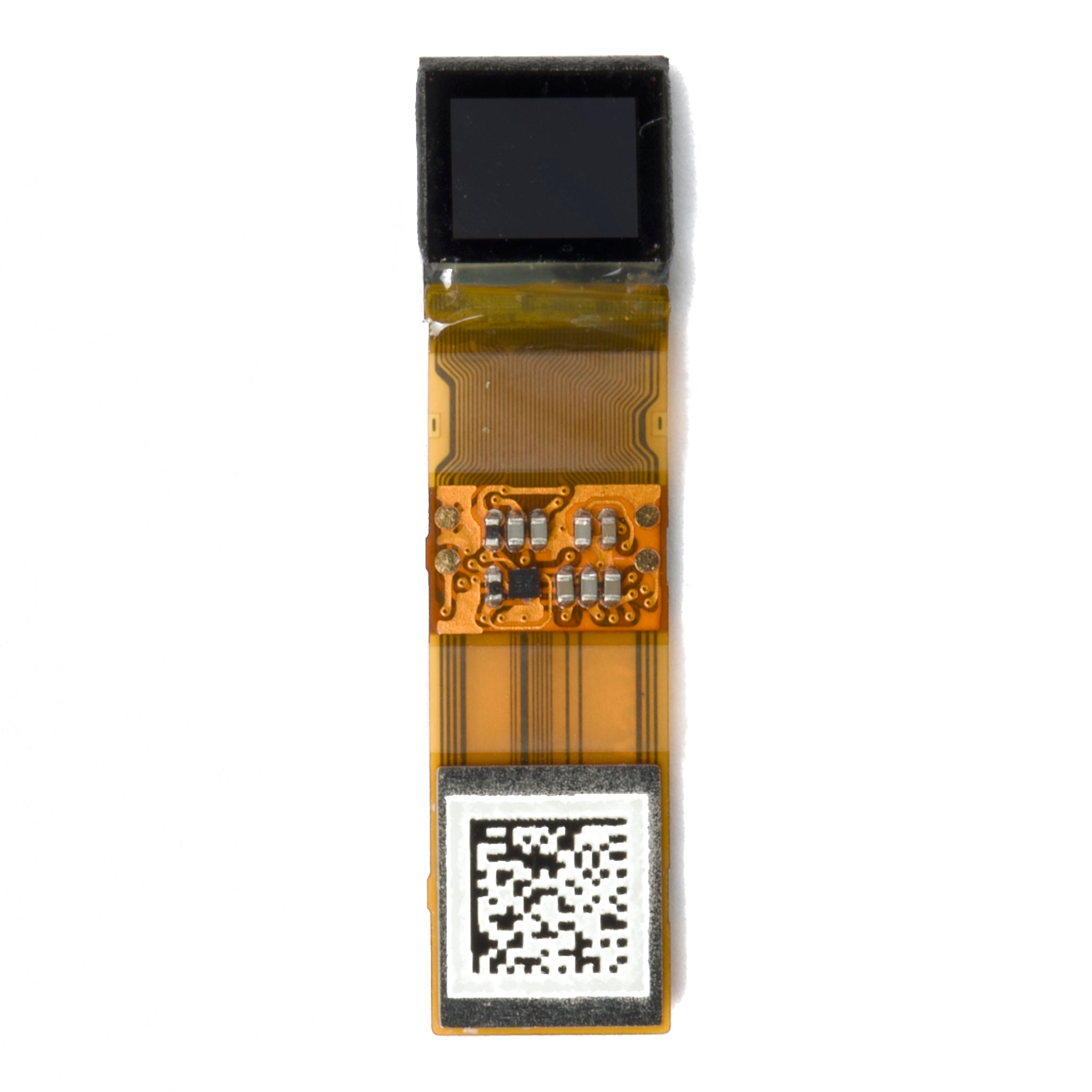
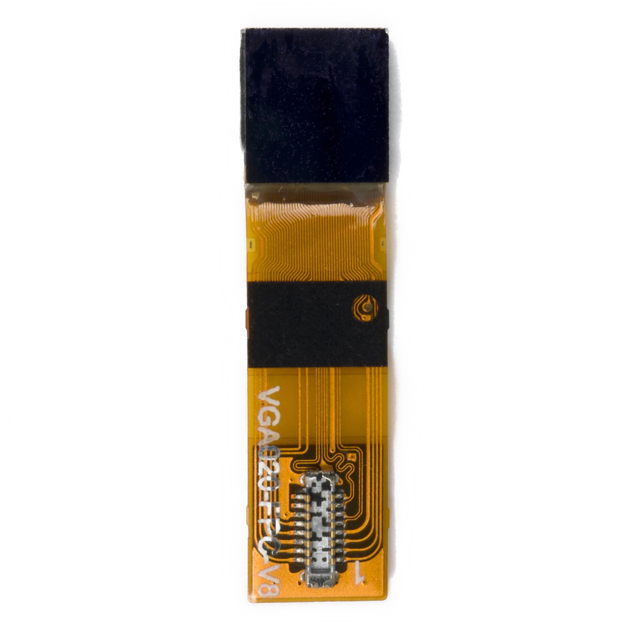
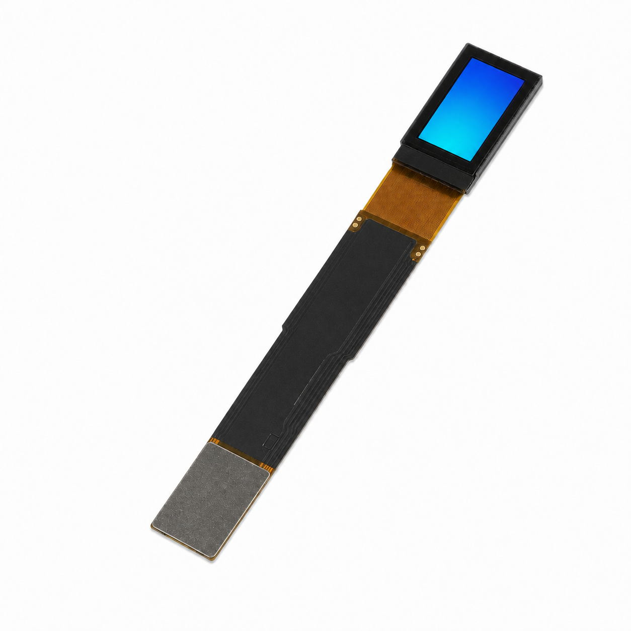
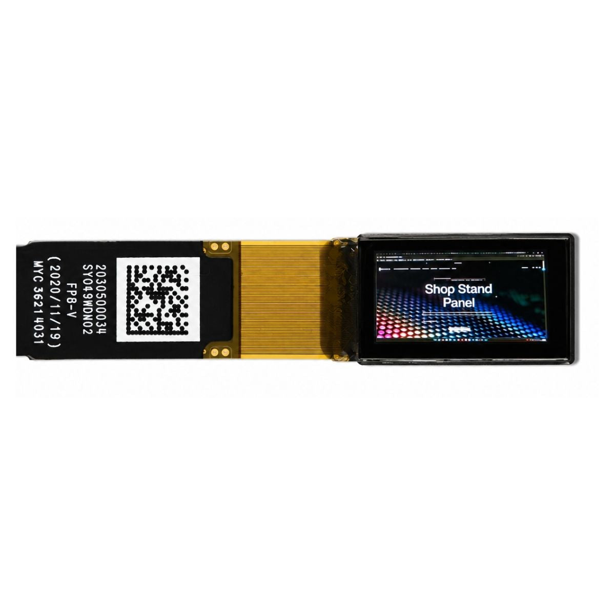
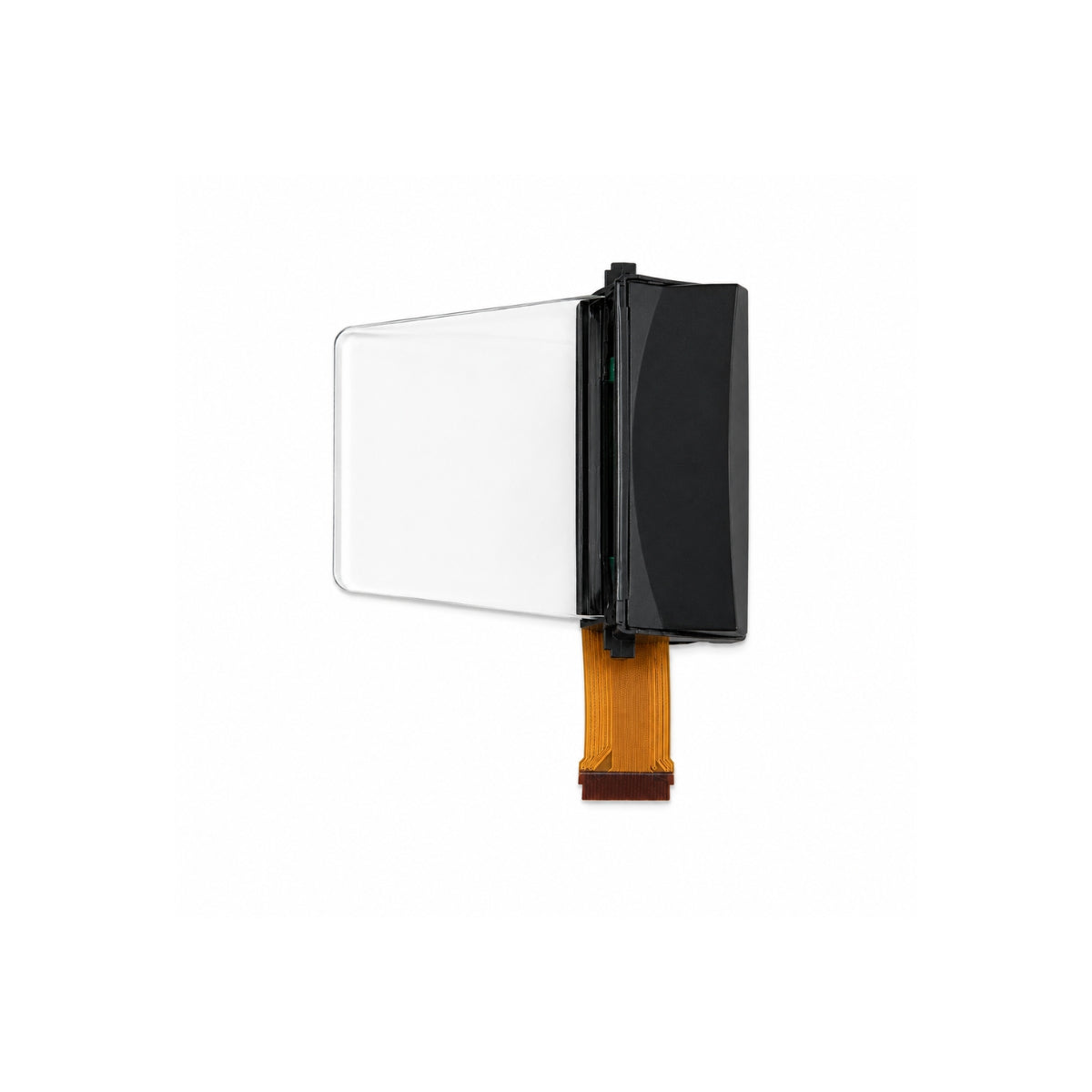
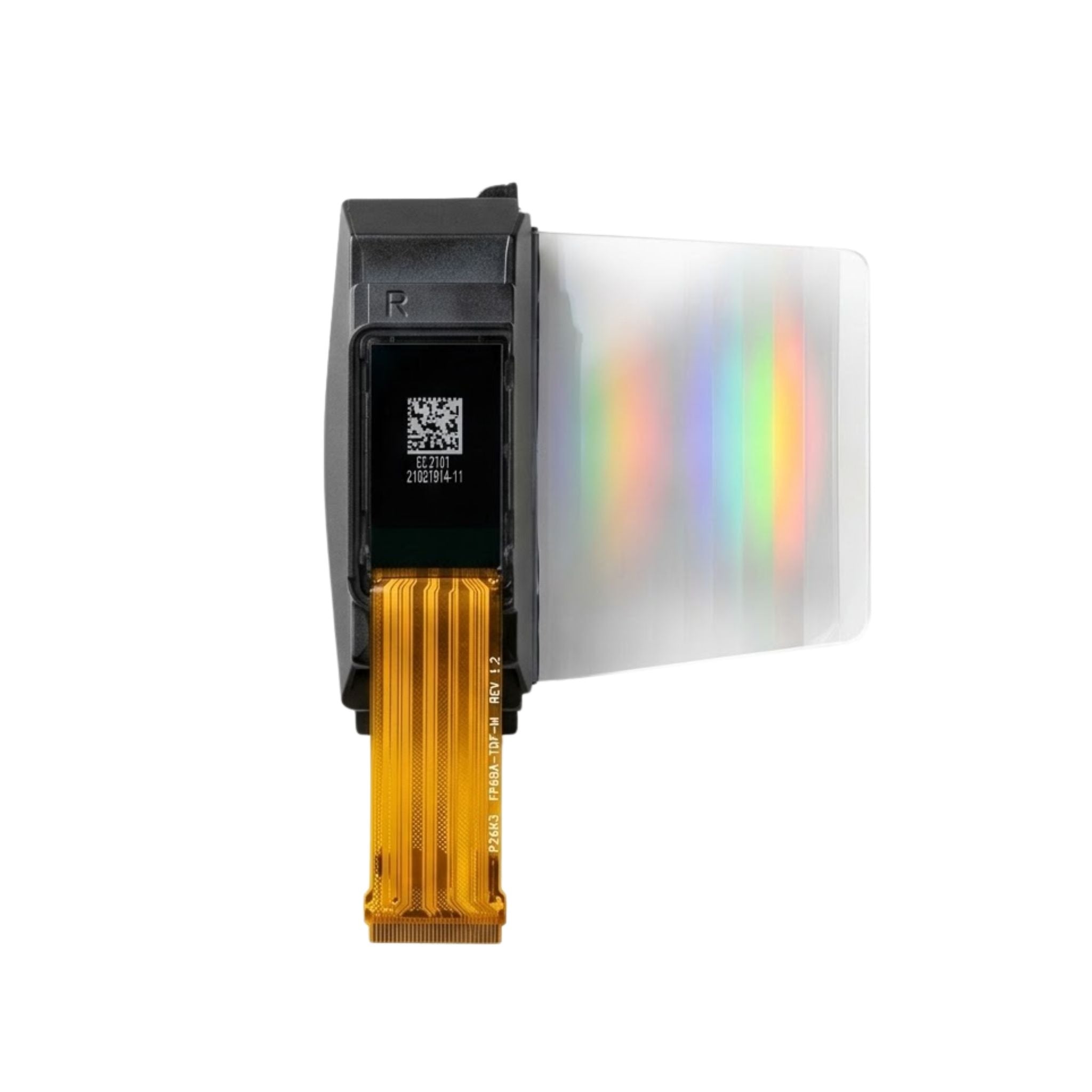


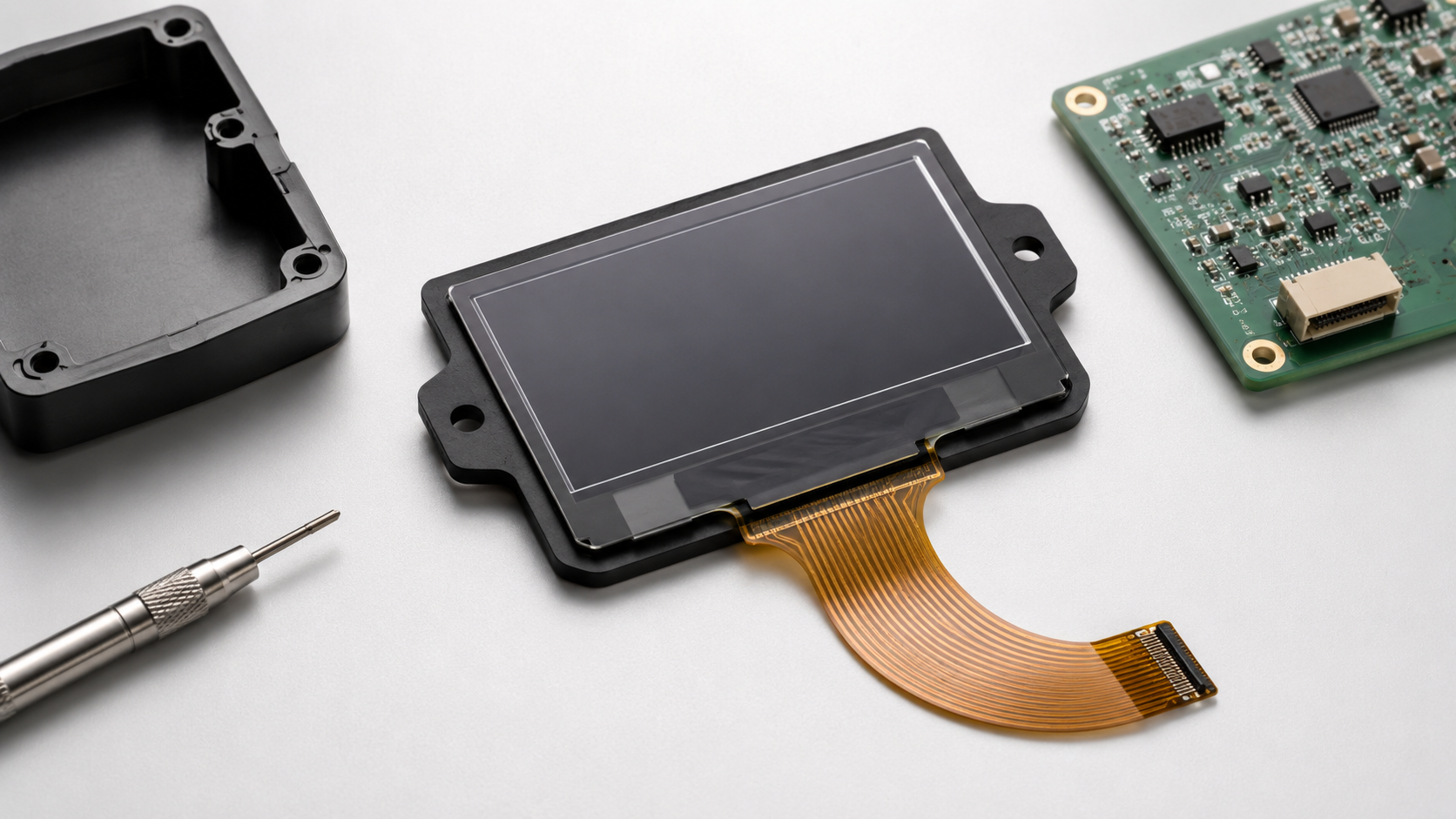
Approve a PMOLED ODM supplier only after the module fits the real enclosure, reaches the production connector without FPC stress, runs with the final firmware, and passes written electrical, optical and reliability limits. A sample that only lights on a test board is not ready for production.
Do Not Use PMOLED for These Loads
PMOLED suits small screens that show text, icons, measurements and simple graphics. Compare another display technology when the product has these operating conditions:
- Fixed bright icons remain on for many hours.
- A large percentage of pixels stays illuminated.
- The display operates nearly 24 hours per day.
- The interface needs video, complex animation or many gray levels.
- The screen must remain readable in strong direct sunlight.
- The same display must remain available for many years without redesign.
- Uneven luminance loss between used and unused areas is unacceptable.
Check existing PMOLED sizes, resolutions and interfaces before paying for new glass. A standard glass panel with a custom FPC usually requires less tooling and less requalification than a completely new OLED cell.
For example, one 0.96-inch 128 × 64 PMOLED has a module outline of 26.70 × 19.26 × 1.40 mm and a listed viewing area of 21.744 × 10.864 mm. The enclosure must use the full drawing rather than the 0.96-inch diagonal alone.
Send These Inputs Before Quotation
| Item | Data Required |
|---|---|
| Resolution | Pixel count, display direction and image orientation |
| Visible area | Required enclosure opening and allowed hidden border |
| Maximum outline | Available length, width and local height |
| FPC | Exit direction, route, bend area and contact-end position |
| Connector | Manufacturer, exact part number, contact side and PCB position |
| Interface | I²C, three-wire SPI, four-wire SPI, 6800-style or 8080-style |
| Power | Logic voltage, OLED drive source, available current and reset control |
| Screen content | Typical UI, fixed icons and expected illuminated area |
| Operating time | Hours per day, idle time and sleep frequency |
| Environment | Operating, storage, humidity, shock and vibration conditions |
| Supply | Prototype quantity, annual demand and required supply period |
“FPC length: 40 mm” is not complete. The supplier must know whether the 40 mm starts at the glass edge, ACF bond edge, first bend line or connector contact end.
“White OLED,” “high brightness,” “SPI interface” and “no pixel defects” are also incomplete. Colour needs an approved range, brightness needs a measurement condition, SPI needs an exact mode, and defects need written pass limits.
Use FPC-Only Customization When the Glass Already Fits
| Change | Parts Affected | Work Required |
|---|---|---|
| Custom FPC | Tail shape, length, pin order, stiffener or connector | FPC drawing, bend check, connector fit and interface test |
| Adapter PCB | Module thickness, connectors and mounting points | Stack-height, power and assembly checks |
| Glass outline | Seal, electrode route, driver area and FPC bond | New tooling, drawing and reliability tests |
| Active area | Pixel position and usable display region | Electrode, optical and driver review |
| Resolution | Pixel matrix, driver, memory and firmware | New mapping, power, lifetime and yield validation |
Use the lowest custom level that meets the enclosure and PCB requirements. If standard glass already fits the visible window, changing only the FPC normally creates less cost and supply risk than changing the glass.
The quotation should separate glass tooling, FPC tooling, test fixtures, sample charges, firmware work and reliability testing. Tool ownership and modification rights should also be written into the quotation. These items are part of the practical cost of custom PMOLED shapes and FPC development.
Put These Dimensions on the Drawing
IEC 62341-1-2:2014 provides preferred OLED terms and definitions so that the supplier and buyer use the same language in drawings and reports.[1]
The drawing must separate:
- Active area: the area containing functional pixels.
- Viewing area: the area intended to be visible through the enclosure window.
- Glass outline: the external size of the OLED glass.
It should also include:
- Active-area position from the locating edges
- Maximum glass length and width
- Maximum local height
- Driver and encapsulation position
- FPC exit centreline
- FPC contact-end position
- Stiffener length, width and thickness
- First allowed bend line
- No-contact and no-bend areas
The enclosure opening should not normally equal the active area exactly. The window may need to hide the inactive border, seal, cutting variation, adhesive position and assembly movement.
Use the same datums in the OLED drawing, enclosure drawing and incoming inspection report. If the enclosure locates the display from the left glass edge, the active-area position should also be controlled from that edge.
During sample fitting, display a one-pixel border and move the module to every position allowed by the enclosure clearance. The full border should remain visible without exposing the seal or driver area.
Leave These Areas Free of Mechanical Pressure
Do not place screws, ribs, clips or hard contact points over:
- The glass edge
- The driver IC
- The encapsulation area
- The FPC-to-glass bond
- The edge seal
The side drawing should show the complete stack:
- Glass thickness
- Driver and encapsulation height
- FPC thickness
- Stiffener thickness
- Components mounted on the FPC
- Adhesive thickness
- Foam, gasket or frame thickness
The 0.96-inch product example has a listed module thickness of 1.40 mm. This does not mean every local point on a custom version will be 1.40 mm. The driver, encapsulation, stiffener or FPC components may create a higher point.
Compare the maximum possible module stack with the minimum available enclosure space. Nominal thickness compared with nominal enclosure depth does not cover tolerance variation.
Specify foam and gasket material, thickness, position and compression. Too much compression can bend the glass. Too little compression can allow movement during shock or vibration.
Run the display before and after all enclosure screws are tightened. Flicker, missing lines or a change when the housing is pressed can indicate mechanical stress.
Fix the FPC Exit Before PCB Release
The FPC drawing must define:
- Exit edge and centreline
- Tail angle, width and length
- Length measurement origin
- Contact side
- Connector insertion direction
- Stiffener dimensions
- First permitted bend line
- Contact-end position tolerance
The tail must reach the connector without pulling the glass away from its locating surface. Do not hide excess FPC length through a sharp fold.
Check the assembly sequence with real parts. The operator must be able to:
- Position the display
- Insert the FPC fully
- Close the connector lock
- Inspect the insertion
- Remove the module without pulling the glass bond
A design can fit in CAD but fail in production because the connector lock is hidden behind a wall or there is no space for a finger or tool.
Define Static and Dynamic Bend Conditions
Draw the full FPC path around ribs, screws, batteries, shields, speakers, motors, antennas and hot components.
Do not route the FPC:
- Across sharp plastic or metal edges
- Under screw bosses
- Between parts that can pinch it
- Across hot components
- Beside high-current switching nodes where avoidable
- Through a path that twists the tail
- Where it rubs during normal use
Request the FPC layer count, copper structure, base-film thickness, coverlay, stiffener material and approved bend direction.
IPC-6013E covers qualification and performance requirements for flexible and rigid-flex boards designed to IPC-2221 and IPC-2223. It also separates boards by performance class and installation use.[2]
A bend formed once during assembly is a static bend. A tail that moves whenever a cover, button or mechanism operates is a dynamic bend.
For dynamic movement, define:
- Minimum bend radius
- Bend angle
- Expected cycle count
- Movement speed
- Operating temperature
- Applied pulling force
Keep components, vias, solder joints, stiffener edges and sudden track-width changes outside the main bend. Do not use a general bend-radius multiplier without checking the actual FPC stack.
Protect the COG and ACF Bond
In COG PMOLED modules that use anisotropic conductive film, the FPC is bonded to conductive pads on the glass. The supplier should control:
- Bond position and width
- Conductive-film specification
- Bonding temperature, pressure and time
- Glass-to-FPC alignment
- Electrical continuity or contact resistance
- Visual inspection limits
- Process-sample pull or peel checks where used
Do not lift the display by the FPC, fold the tail against the bond edge or pull the module from the enclosure by its tail.
Missing rows or columns that change when the FPC is touched can come from the glass bond, connector, FPC tracks or driver connection. Check each part before assigning the cause.
Match the FPC to the Exact Connector
Matching contact pitch alone does not prove that the FPC fits the connector.
Confirm:
- Connector manufacturer and part number
- Contact count and pitch
- Supported FPC thickness
- Top-contact or bottom-contact construction
- Exposed contact length
- Insertion depth
- Stiffener thickness
- Lock type
- Rated mating cycles
Test the production FPC with the production connector mounted on the production PCB. Check that the exposed contact reaches the terminal position and that closing the lock does not buckle the stiffener.
The FPC drawing should show the contact side from a clearly labelled viewing direction. Avoid terms such as “same side” and “reverse side” unless the view direction is also shown.
Freeze Pinout, Voltage Domains and View Direction
| Pin Field | Required Detail |
|---|---|
| Pin number | Numbered from a stated viewing direction |
| Signal | Exact driver or module signal name |
| Direction | Input, output, bidirectional, power or ground |
| Voltage | Logic domain and maximum allowed level |
| Power state | Required level during startup and shutdown |
| Unused pin | Floating, grounded, reserved or internally unconnected |
Explain VCC, VDD, VPP and NC in the pin table. An NC pin may be internally open, reserved or required to remain floating.
Confirm whether interface inputs tolerate the host voltage and whether signals may remain high while the display supply is off. Add a level shifter when the voltage domains do not match.
Before first power-on, check pin 1 on the FPC, connector and PCB together. Confirm whether every drawing is viewed from the display side, component side or contact side.
Confirm Driver, Interface and RAM Mapping
Request these driver details:
- Exact driver part number
- Interfaces connected on the module
- Display RAM map
- Column and row offsets
- Segment remap and scan direction
- Multiplex ratio
- Charge-pump settings
- Contrast or current range
- Reset and startup timing
Small PMOLEDs can require very different electrical designs. The 0.96-inch 128 × 64 example uses a monochrome matrix and supports SPI or I²C. By comparison, one 1.1-inch colour PMOLED uses a 96(RGB) × 96 matrix, supports up to 65,536 colours, has a 25.90 × 30.10 × 1.30 mm panel and a 19.852 × 19.852 mm active area.
The 1.1-inch product lists a 2.8 V logic supply and a 12.0 V OLED supply. A small PMOLED therefore does not always use one low-voltage rail.
For SPI, define:
- Three-wire or four-wire operation
- Clock polarity and phase
- Bit order
- Chip-select behaviour
- Data/command control
- Tested clock rate
- Required command delays
For I²C, define:
- Device address
- Tested bus speed
- Pull-up voltage and resistor location
- Bus capacitance
- Readback support
- Recovery method when SDA remains low
The supplier should provide initialization code tested on the proposed sample. Code copied from another display with the same resolution may still use the wrong column offset, scan direction or charge-pump settings.
Pin count, update time and bus loading can be compared in the practical differences between SPI and I²C OLED interfaces.
| Symptom | First Checks |
|---|---|
| Black screen | Power, reset, initialization and display-on command |
| Shifted image | Column offset and RAM mapping |
| Mirrored image | Segment remap |
| Upside-down image | COM scan direction |
| Random pixels | Bus timing, grounding and supply noise |
| Black screen after wake | Power state, bus condition, reset and reinitialization |
Record Power in Six Operating States
Do not treat Display OFF and Sleep as the same state. Display OFF may stop pixel output while the controller remains powered. Sleep or power-save mode may disable more internal circuits.
| Mode or Pattern | Data to Record |
|---|---|
| Display OFF command | Current with pixel output disabled |
| Sleep or power-save mode | Current after the approved sleep sequence |
| Normal production UI | Typical operating current |
| High pixel-on pattern | Current under a heavily illuminated image |
| Supplier-defined worst case | Maximum expected current for the approved configuration |
| Repeated updates | Supply and bus behaviour during data transfer |
The 0.96-inch 128 × 64 product example lists a typical operating current of 12.3 mA. This value applies to that module and its stated conditions. A custom version must be measured again with the approved contrast setting and production UI.
An all-pixel pattern is useful but is not automatically the worst electrical condition. Current also changes with the driver, contrast setting, multiplex ratio, charge pump, temperature and update activity.
IEC 62341-6-1:2025 specifies measurement methods for OLED optical and electro-optical parameters, including power consumption. Record the supply voltage, test pattern, driver setting, temperature and instrument with every result.[3]
Battery products should be tested at full, normal and minimum operating voltage while radios, motors or other high-load circuits are active.
Run Startup, Sleep and Noise Tests on the Final PCB
Test these states:
- Cold start
- Warm restart
- MCU starting before the display
- Display starting before the MCU
- Short power interruption without complete discharge
- MCU watchdog reset
- Interrupted SPI or I²C transfer
- Repeated sleep and wake cycles
- Recovery after a bus timeout
As an initial engineering check, run at least 100 consecutive power-on, reset and initialization cycles on the final PCB. Record each black screen, failed reset, shifted image or abnormal startup. The 100-cycle value is a project starting point, not an IEC requirement.
For products that regularly use sleep mode, run at least 100 consecutive sleep-and-wake cycles, then continue with a longer normal-use test. When an I²C display fails after sleep, record the supply, reset pin, SDA, SCL and address acknowledgement before restarting the system. A practical fault-isolation sequence is available in the article about an I²C OLED that stops responding after repeated sleep cycles.
Run the display while motors, relays, radios, chargers and DC/DC converters operate. Watch for resets, flicker, corrupted pixels, missing lines and bright flashes during shutdown.
Finished-product ESD testing must use the real enclosure, grounding path and user-accessible surfaces. IEC 61000-4-2:2025 defines test methods for equipment exposed to electrostatic discharge, while the applicable product standard sets the test level and pass criteria.[4]
Set Lifetime Rules from the Actual UI
Record the daily display time and the longest continuous time for:
- Logos
- Battery icons
- Menu bars
- Warning frames
- Fixed units and labels
Image sticking is a residual image that may reduce after recovery. Differential ageing is a lasting luminance difference between areas that received different use.
A supplier lifetime statement should include:
- The end point, such as L50, L70 or another defined limit
- Initial luminance
- Test temperature
- Image pattern and illuminated area
- Driver setting
- Operating duty
- Whether the result is measured or estimated
IEC 62341-5-3:2019 specifies methods for measuring OLED image sticking and lifetime. Do not compare two lifetime numbers unless their test conditions are also compared.[5]
Where the interface allows it, reduce long-term stress by lowering normal brightness, switching the display off during long idle periods and moving fixed elements slightly.
Write Optical and Defect Acceptance Limits
Replace “bright,” “uniform,” “clear” and “no obvious defects” with written limits.
Define:
- Initial luminance
- Measurement points
- Uniformity calculation
- Display colour or chromaticity range
- Viewing direction
- Test pattern
- Warm-up time
- Ambient condition
- Driver and contrast setting
IEC 62341-6-3:2017 provides OLED image-quality measurement methods, including viewing-angle, colour and resolution measurements.[6]
For a small PMOLED, a five-point measurement is a useful starting method:
- Centre
- Upper left
- Upper right
- Lower left
- Lower right
Use the same pattern, voltage, contrast setting, warm-up time and instrument at all five points.
| Defect Group | Examples |
|---|---|
| Functional | Missing row, missing column, flicker or initialization failure |
| Pixel | Bright, dark, adjacent or unstable pixels |
| Optical | Uneven luminance, colour difference or image sticking |
| Cosmetic | Scratch, glass chip, contamination or surface-film damage |
| Mechanical | Creased FPC, damaged stiffener or lifted bond |
The inspection method should state the viewing distance, lighting, angle, pattern and observation time. A phone camera can record a visible fault but cannot replace a controlled luminance or colour measurement.
Use Separate Samples for Fit, Function and Reliability
| Sample Stage | Work Required |
|---|---|
| Fit samples | Window alignment, stack height, FPC route and connector access |
| Function samples | Firmware, interface, power, reset and optical checks |
| Reliability samples | Separate units for temperature, humidity, shock, vibration and ageing |
| Pilot lot | Production variation, yield, defects and packaging |
| Retained samples | Approved and untested references from the accepted lot |
Do not reuse one module for several destructive tests. Keep untested control samples from the same production lot.
The fit test should confirm that:
- The glass sits flat without forced insertion.
- The complete active area remains visible.
- The housing does not touch the driver or bond area.
- The FPC reaches the connector without tension.
- The connector lock closes fully.
- The module can be removed without pulling the FPC.
The function report should record the sample number, lot, drawing revision, firmware revision, driver, voltage, current, pattern, optical result and failure reason.
Use full-off, full-on, one-pixel-border, vertical-line, horizontal-line, checkerboard and moving-pixel patterns to expose mapping and connection faults.
Apply Environmental Tests to the Failure Risk
IEC 62341-5-2:2019 covers mechanical endurance testing for OLED panels, modules and packaged forms and uses IEC 60068 methods where applicable.[7]
| Test | Items to Check |
|---|---|
| Low temperature | Startup, luminance, charge pump and connection stability |
| High temperature | Luminance, current, adhesive, seal and image retention |
| Temperature change | Stress between glass, FPC, bond, adhesive and enclosure |
| Damp heat | Seal, corrosion, bonding and intermittent faults |
| Vibration | Glass support, connector lock and FPC tension |
| Shock | Glass cracks, edge contact and module movement |
IEC 60068-2-1:2025 and IEC 60068-2-2:2025 provide cold and dry-heat test methods.[8][9]
IEC 60068-2-14:2023 covers temperature-change testing, while IEC 60068-2-78:2025 covers steady damp heat without condensation.[10][11]
IEC 60068-2-6 and IEC 60068-2-27 provide sinusoidal vibration and shock test methods.[12][13]
The project must still define the temperature, humidity, duration, powered state, mounting condition, sample quantity and pass criteria.
Create electrical, optical and visual baseline records before testing. After the required recovery period, repeat the same measurements. Do not pass a sample only because it still turns on.
Use Pilot Data, Golden Samples and Traceability
Measure pilot samples from the beginning, middle and end of the production run.
Compare:
- Active-area position
- FPC length and exit position
- Stiffener position
- Total thickness
- Luminance
- Operating current
- Connector fit
- Bond appearance
Also record first-pass yield, rework, scrap and defect categories. Do not approve the pilot lot from one average value. A wide spread can show weak process control even when each sample remains inside a loose limit.
For a small industrial project, keeping 3–5 approved and untested modules is a practical starting point. Keep at least:
- One functional golden sample
- One appearance sample
- One untested retained sample
- Acceptable and unacceptable boundary samples where available
Each module should be traceable to its part number, drawing revision, production date, glass lot, driver lot, FPC lot, bonding material and outgoing inspection result.
Require Evidence Before Supplier Approval
ISO 9001:2015 defines requirements for a quality management system, but certification alone does not prove that a PMOLED meets its drawing or reliability limits.[14]
| Supplier Claim | Evidence Required |
|---|---|
| Custom outline capability | Controlled drawing or a redacted similar project |
| FPC design control | Released FPC drawing, stack and bend review |
| Bonding control | Process limits, inspection method and records |
| Reliability testing | Test method, sample list, conditions and results |
| Firmware support | Initialization code tested on the proposed module |
| Outgoing inspection | Inspection limits and traceable reports |
| Long-term supply | Driver status, glass-platform status and change process |
Ask which operations are completed internally and which are outsourced. Outsourcing is acceptable when the ODM supplier controls the drawings, materials, process, inspection and changes.
Compliance documents should identify the exact module part number and revision. The EU RoHS Directive currently restricts ten substances in electrical and electronic equipment.[15]
Request the REACH and SVHC information required for the target market and customer supply chain. REACH regulates chemical substances used and supplied in the EU.[16]
Lock Changes, EOL and Corrective Action
Require written notice before changing:
- OLED material or glass source
- Driver IC
- Glass or electrode layout
- FPC material or copper structure
- Stiffener or contact finish
- Bonding material or process
- Adhesive or encapsulation
- Production location
- Inspection method
The notice should state the old configuration, new configuration, reason, first affected lot, comparison results and required customer approval.
The supply agreement should also define:
- Driver and glass end-of-life notice
- Last-time-buy date
- Last shipment date
- Replacement sample process
- Firmware-change responsibility
- Requalification responsibility
When a failure occurs, record the module lot, firmware, voltage, image pattern and whether touching the FPC changes the fault. Preserve the failed state before repeatedly reinserting or bending the module.
The supplier’s corrective-action report should state:
- What failed
- Which lots are affected
- The confirmed cause
- The temporary containment
- The permanent correction
- The test proving that the correction works
Send One Complete RFQ
- Resolution, colour, orientation and active area
- Maximum outline, thickness and window position
- Mechanical datums and no-contact areas
- FPC exit, route, bend type and connector
- Pinout and voltage domains
- Driver, interface and reset sequence
- Typical screen content and daily operating time
- Operating and storage environment
- Power, optical and defect limits
- Prototype, pilot and annual quantities
- Sample validation and environmental test plan
- Traceability and failure-analysis requirements
- Supply-life and change-notice requirements
- Compliance documents
- Tooling and design-file ownership
Put every supplier assumption on the quotation or controlled drawing. Do not leave important dimensions, voltage conditions or acceptance limits only in emails or meeting notes.
Finally
Release the PMOLED only when the glass drawing, FPC drawing, pinout, driver settings and firmware use the same revision. Check the maximum module stack against the minimum enclosure space, and keep all bends away from the glass bond. Run at least 100 startup cycles and 100 sleep/wake cycles as an initial engineering check. Measure luminance at five points, use separate modules for destructive tests, and compare pilot samples from the beginning, middle and end of production. Keep 3–5 approved samples, require lot traceability and block material, driver or process changes until the new version has passed the agreed tests.
Leave a comment
This site is protected by hCaptcha and the hCaptcha Privacy Policy and Terms of Service apply.