

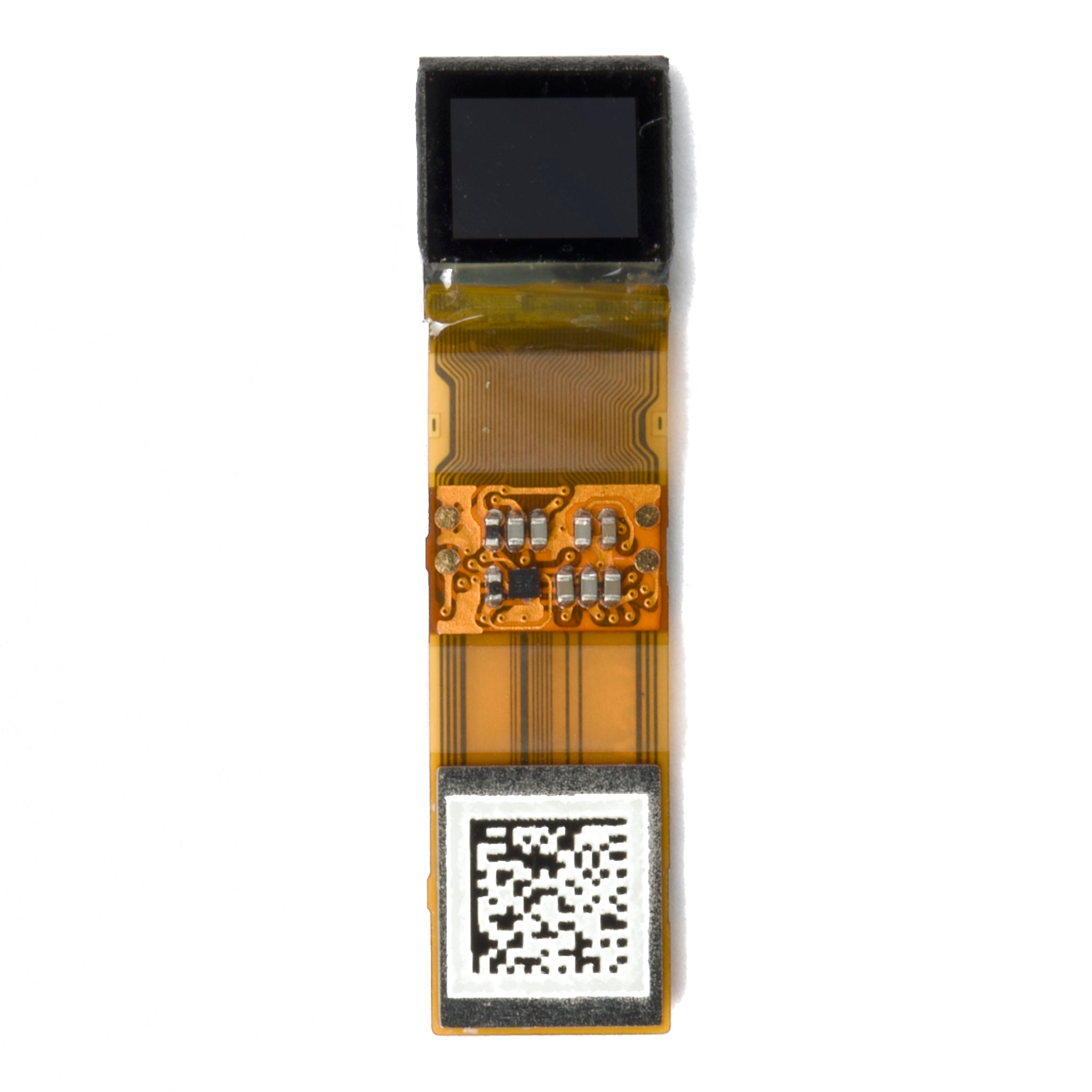
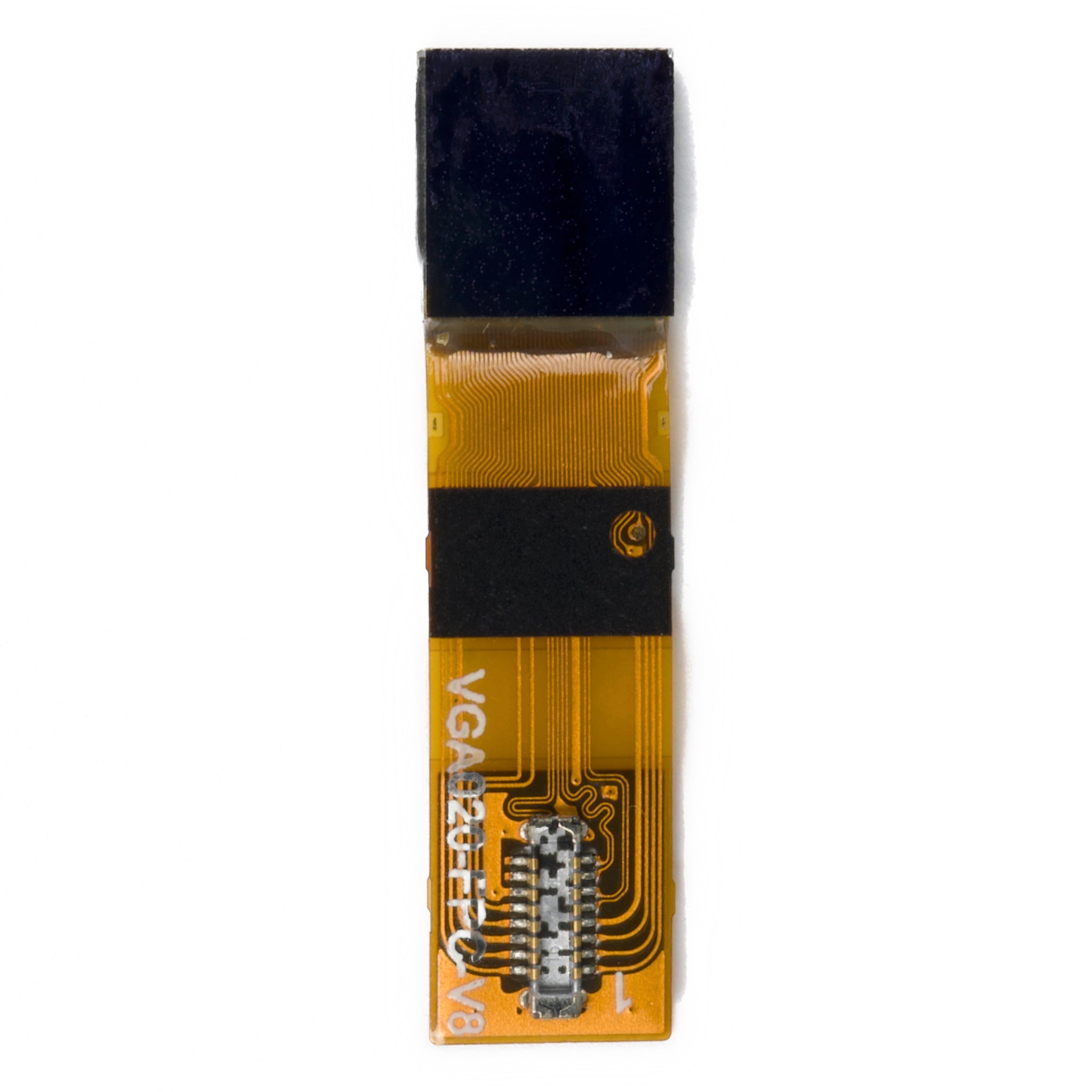
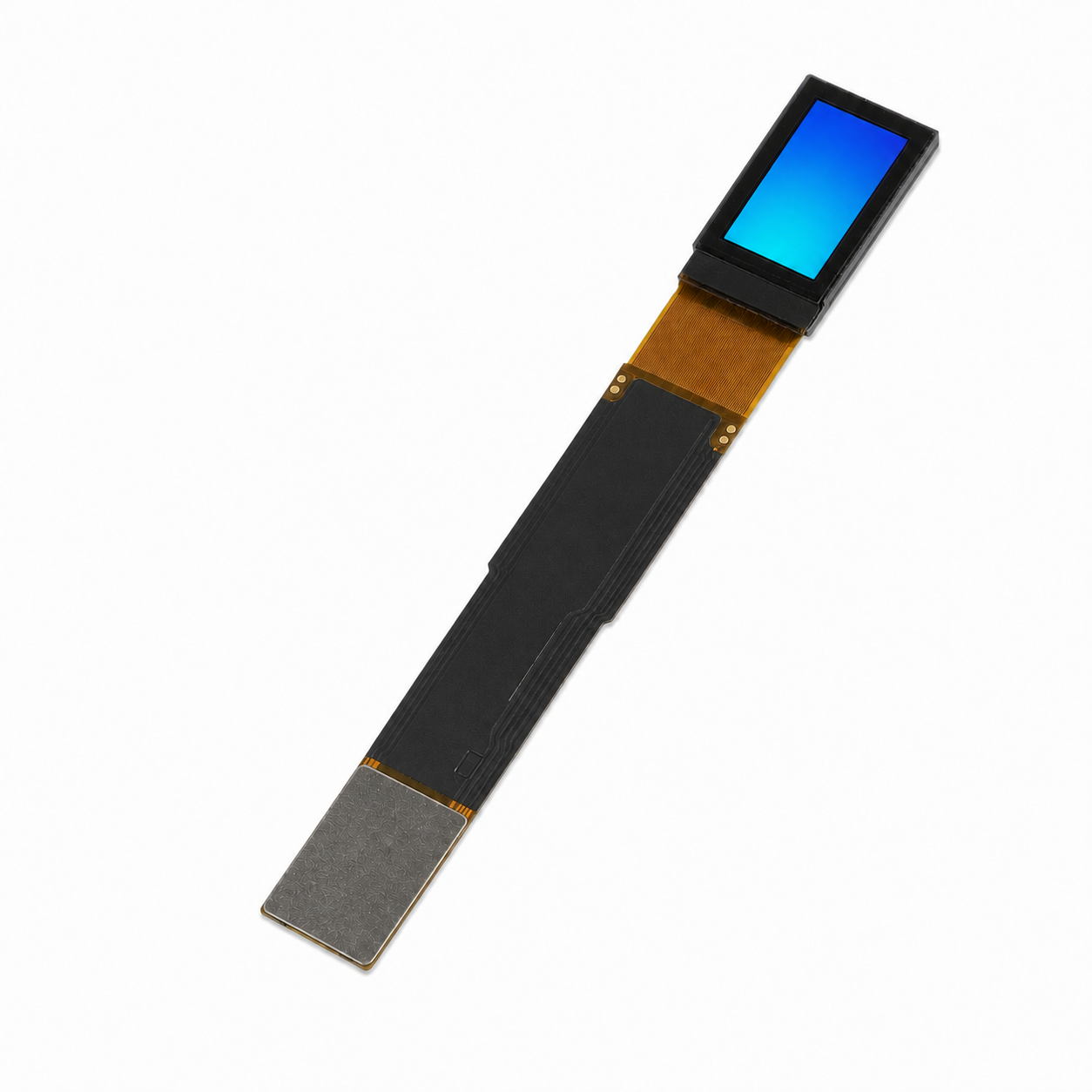
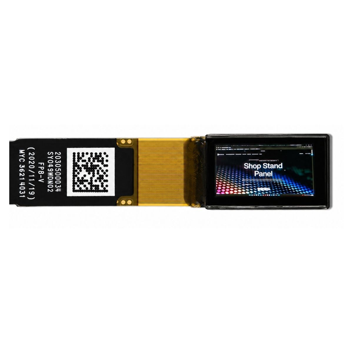


Set the connector coordinates from fixed datums, measure power and signals at the module end, and test cold startup, EMI, ESD and vibration with the final enclosure. For a 128 × 64 monochrome PMOLED, one full frame contains 1,024 bytes; the raw transfer time is about 23 ms at 400 kHz I²C and 1.0 ms at 8 MHz SPI.
Required Project Data
| Item | Required value | Approval evidence |
|---|---|---|
| Resolution | Pixel count and display orientation | Module drawing and firmware test |
| Active area | Illuminated width and height | Controlled mechanical drawing |
| Viewing area | Visible opening behind the front window | Enclosure drawing and fit sample |
| Module outline | Maximum width, height, thickness and flatness | Drawing and incoming inspection |
| Connector | Manufacturer, part number, pitch and contact direction | Connector specification |
| FPC | Exit side, length, thickness, stiffener and bend area | FPC drawing and assembly sample |
| Interface | SPI, I²C, 6800, 8080 or another supported mode | Pin table and communication test |
| Logic level | Guaranteed VOH, VOL, VIH and VIL limits | MCU and display specifications |
| Power | Minimum, nominal and maximum module-end voltage | Oscilloscope and current measurements |
| Luminance | Minimum value under a defined image and drive setting | Optical test report |
| Temperature | Operating, storage, cold-start and hot-start limits | Environmental test report |
| Mechanical load | Vibration, shock, cable movement and mounting pressure | Mechanical qualification report |
| Operating life | Hours, luminance, temperature and screen-content conditions | Supplier life-test definition |
| Supply period | Required production years, PCN period and EOL notice | Supply agreement |
Use the exact module specification rather than a general PMOLED assumption. The 2.4-inch 128 × 64 PMOLED display, for example, lists a 60.5 × 55.6 × 2.01 mm module outline and a −40°C to +70°C operating range. A smaller 1.3-inch 128 × 64 SPI/I²C OLED module requires a different PCB, window and cable layout.
Standard Module or Custom Part
| Condition | Action |
|---|---|
| The standard outline and connector fit the device | Use the standard module |
| A small main-PCB movement solves the fit problem | Modify the main PCB |
| The FPC exits toward a rib, battery or bracket | Change the FPC exit direction or length |
| The connector cannot be reached during service | Move the connector or change the connection type |
| The module does not meet the required temperature range | Select a qualified module or develop a new configuration |
| The pinout conflicts with an existing controller board | Compare a custom module with a controller-board revision |
Connector Drawing Data
Dimension the connector from two fixed edges, centerlines or another approved datum. Do not control its position with a photograph.
- Connector center coordinates
- Pin 1 position
- Top-contact or bottom-contact type
- FPC contact direction
- FPC insertion direction
- Latch opening direction
- Maximum closed height
- Maximum open-latch height
- Insertion depth
- Component keep-out area
- Cable removal space
Show the connector with its latch open in the enclosure model. The technician must be able to open the latch, hold the FPC stiffener and pull the cable straight out without pressing the OLED glass.
Do not place the connector directly behind a battery, screw boss, metal shield, structural rib, second PCB or high-voltage terminal.
Connector Tolerance Calculation
Use only dimensions that belong to the same datum chain. The following values are a project example:
- Module position: ±0.30 mm
- Connector position: ±0.20 mm
- Main-PCB position: ±0.25 mm
- Enclosure support position: ±0.20 mm
0.30 + 0.20 + 0.25 + 0.20 = 0.95 mm
The connector can move as much as 0.95 mm from its nominal position in one direction. The full range between opposite tolerance limits is:
0.95 × 2 = 1.90 mm
A nominal side clearance of 0.50 mm would not be enough in this example. Increase the available clearance or reduce the individual tolerances.
Connector Retention
For a module exposed to vibration or repeated service, define:
- Required mating cycles
- Maximum contact resistance
- Latch holding condition
- FPC insertion mark
- Reverse-insertion prevention
- Cable clamp or strain-relief position
- Replacement rule after latch or contact damage
Use the connector manufacturer’s mating-cycle and contact-resistance limits. Cable bend radius and strain relief should also be controlled in the assembly instructions.[1]
FPC Route and Bend Limits
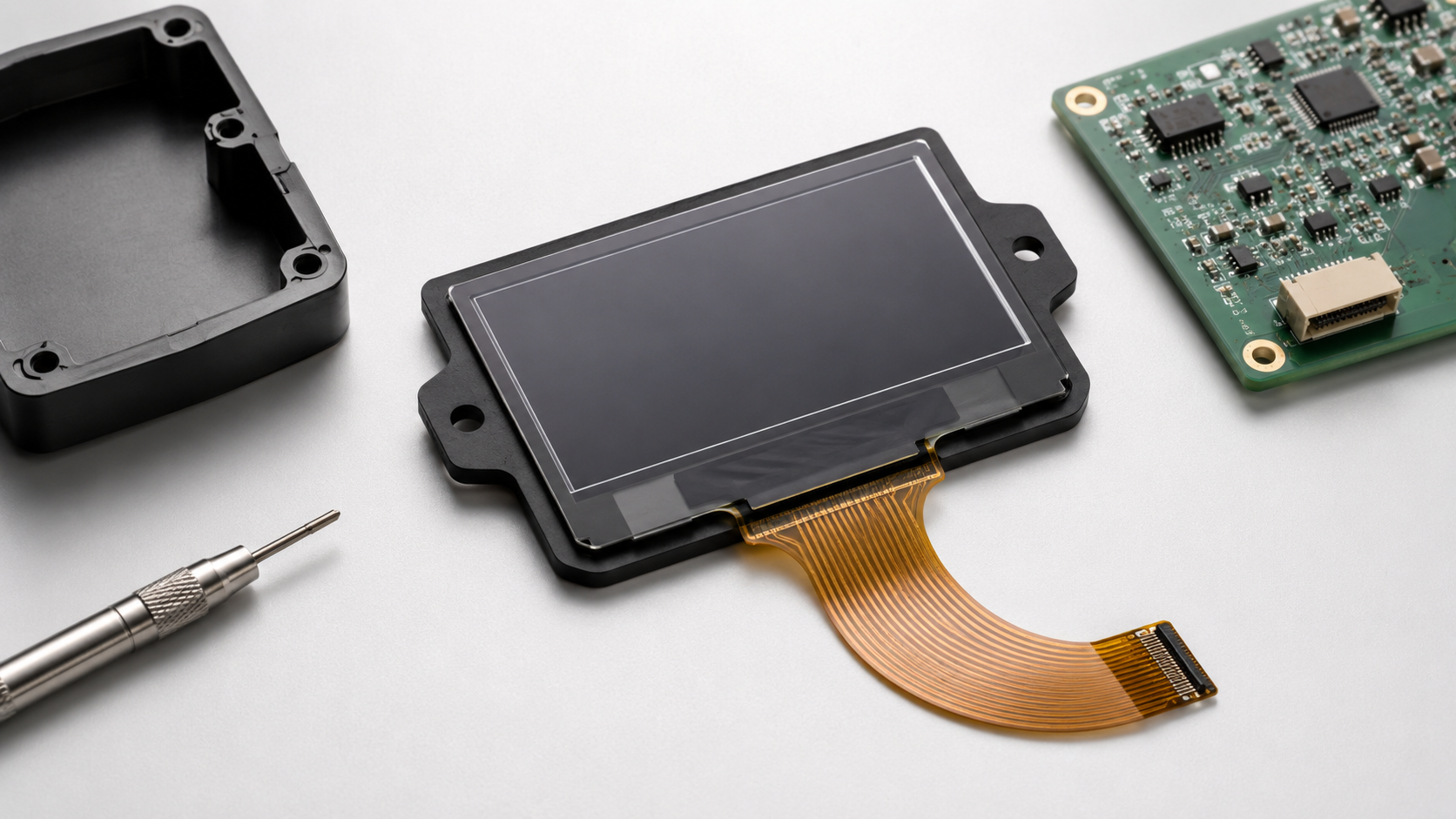
The FPC drawing should mark the glass-bond area, connector stiffener, approved bend area, no-bend area and strain-relief point.
Do not bend the FPC at:
- The glass bond
- The stiffener edge
- A solder joint
- A mounted component
- A narrow cable neck
A static bend is formed during assembly and remains still. A dynamic bend moves during normal operation. A dynamic-flex requirement should state the bend radius, angle, travel distance, speed, cycle count, test temperature and maximum conductor-resistance change.
Keep the FPC away from switching inductors, motor wires, solenoids, relay contacts, high-current battery wires, RF antennas and sharp metal edges. If it must cross a noisy cable, keep the crossing short and close to 90 degrees.
Define minimum and maximum installed slack. A short FPC can pull on the glass bond; an excessively long FPC can rub against the enclosure or move during vibration.
FPC Voltage Drop
Measure the supply at the module connector while the highest-current screen is active.
Project example:
- Regulator output: 3.30 V
- PCB, connector and FPC loss: 0.10 V
- Module-end voltage: 3.20 V
3.30 V − 0.10 V = 3.20 V
The voltage loss is about 3.0% of the nominal supply:
0.10 ÷ 3.30 × 100% ≈ 3.0%
Check whether 3.20 V remains above the module’s guaranteed minimum during startup, full-screen updates, motor operation and the lowest device input voltage.
Review FPC copper thickness, power-trace width, ground-trace width, cable length and connector contact resistance. Do not add shielding unless testing shows it is needed. A shield changes FPC thickness, stiffness, grounding and bend radius.
Pinout and Boot States
The pin table should include:
- Logic supply
- OLED supply, if separate
- Ground
- Clock
- Data
- Chip select
- Data/command
- Reset
- Read/write
- Interface-selection pins
- Address-selection pins
- Reserved pins
- No-connect pins
State whether every unused pin must be tied high, tied low, held by a resistor or left open. Do not leave interface-selection pins floating.
Where the controller and connector allow it, place ground conductors near fast signals. The following is an example, not a standard pinout:
GND – CLK – GND – DATA – GND – CS – DC – RESET
Measure reset, chip select and interface-selection pins while the MCU is starting. These pins may be high impedance before firmware configures them. Also check whether a powered MCU can back-power an unpowered module through an interface pin.
Interface Data Rate
The display interface guide compares 6800, 8080, SPI and I²C connections. For a small industrial PMOLED, choose the interface from the required update time, available MCU pins, cable length and measured signal quality.
| Interface | Use case | Main limit |
|---|---|---|
| I²C | Slow status screens with limited MCU pins | Lower full-frame speed |
| SPI | Faster serial updates | Clock ringing on long routes |
| 6800 | Existing 6800-compatible host | More signal conductors |
| 8080 | Fast parallel transfer | Larger connector and routing area |
A 128 × 64 monochrome frame contains:
- 8,192 pixels
- 8,192 bits
- 1,024 bytes
At 400 kHz I²C, using nine clocks per transferred byte:
1,024 × 9 ÷ 400,000 = 0.02304 seconds
The raw transfer time is about 23.0 ms, giving a theoretical data-only limit of about 43.4 full frames per second.
At 8 MHz SPI:
1,024 × 8 ÷ 8,000,000 = 0.001024 seconds
The raw transfer time is about 1.0 ms. Commands, MCU processing, addressing and driver limits reduce the real update rate. The SPI and I²C comparison covers the related speed and pin-count tradeoffs.
Logic-Level Margin
Compare the guaranteed values, not the nominal supply labels.
- MCU output-high minimum: VOH
- MCU output-low maximum: VOL
- Display input-high minimum: VIH
- Display input-low maximum: VIL
Calculation example:
- Display supply: 3.3 V
- Display VIH: 0.8 × VDD
- Required high level: 2.64 V
- MCU guaranteed VOH: 2.40 V
0.8 × 3.3 V = 2.64 V
The MCU output is not guaranteed to meet the display input requirement. Use a compatible I/O supply, level shifter or another approved circuit.
Measure clock, data and chip select at the display connector. Record overshoot, undershoot, ringing, rise time and setup or hold-time margin.
Power Budget
Measure current with the following production patterns:
- All pixels off
- Normal interface screen
- 50% checkerboard
- All pixels on
- Maximum approved contrast
- Rapid full-frame updates
- Cold startup
- Hot operation
Project example:
- Highest measured display current: 120 mA
- Allocated display current: 150 mA
- Current headroom: 30 mA
150 mA − 120 mA = 30 mA
30 ÷ 120 × 100% = 25%
The 25% headroom is an example, not a universal PMOLED rule. The final supply must also cover regulator tolerance, temperature, cable loss and other loads on the same rail.
Startup and Brownout Test
Record the approved order and timing for:
- Supply rise
- Reset assertion
- Reset release
- Delay before the first command
- Interface setup
- OLED-voltage setup
- Contrast setup
- Display-on command
- First frame write
Repeat startup at minimum voltage, maximum voltage, cold temperature and hot temperature. Also test slow supply decay, short power interruption and brownout.
Monitor for:
- Random illuminated pixels
- Controller lockup
- Back-powering through signal pins
- Incomplete reset
- Failure after a short off-time
Communication Endurance Test
One practical project test is 1,000 complete 128 × 64 frame transfers at the approved interface speed:
1,000 × 1,024 bytes = 1,024,000 bytes
Record:
- Communication timeouts
- Missing acknowledgements
- Corrupted frames
- Unexpected resets
- Minimum module-end voltage
- Driver error counters
An example acceptance limit is zero communication errors and zero unintended resets during the 1,000-frame test. Set the real cycle count from the product reliability plan.
Brightness and Static Content
Measure module temperature and luminance inside the final enclosure with the processor, regulator and other heat sources active.
- Use normal brightness for continuous operation.
- Use maximum brightness only for short alarm periods.
- Dim the display after inactivity.
- Turn the display off when no information is needed.
- Reduce brightness when the internal temperature rises.
- Move or alternate fixed borders, menu bars and alarm fields.
Use the real production interface during endurance testing. The PMOLED lifespan article provides additional screen-management options, but the final values must be verified on the selected module.
Heat, moisture, oxygen, impurities and electrical stress can contribute to OLED luminance loss and failure.[2]
EMI Layout Controls
For measurement, control and laboratory equipment, IEC 61326-1 defines general EMC emission and immunity requirements. Use the standard that applies to the finished product and target market.[3]
| EMC area | Display-related fault |
|---|---|
| Radiated emissions | Clock or converter frequencies appear in an emissions scan |
| Conducted emissions | Display-current ripple reaches an external cable |
| Radiated immunity | Frozen image, reset or corrupted data |
| Conducted immunity | Missing pixels or interface failure |
IEC 61000-4-3 covers radiated RF immunity.[4] IEC 61000-4-4 covers electrical fast transients.[5] IEC 61000-4-5 covers surge immunity.[6] IEC 61000-4-6 covers conducted RF immunity.[7]
- Place bypass capacitors close to controller and converter power pins.
- Keep the power-to-capacitor-to-ground loop short.
- Do not route clock, data or reset across a split reference plane.
- Keep converter switch-node copper small and away from display signals.
- Keep the FPC away from motor, relay, solenoid and antenna wiring.
- Measure clock and supply at the display connector.
Provide one source-series resistor position near the MCU. Candidate values may include 0 Ω, 22 Ω, 33 Ω and 47 Ω. Select the final value from the measured waveform and timing margin.
A ferrite bead must be checked for current rating, DC resistance, impedance curve, surrounding capacitance and voltage drop. It is not a complete filter by itself.
EMI Pre-Scan Conditions
- All pixels on
- Checkerboard image
- Rapid black-to-white changes
- Continuous full-frame updates
- Maximum approved contrast
- Repeated sleep and wake
- Minimum and maximum input voltage
- Motor, relay and radio operation at the same time
Record the firmware version, interface frequency, FPC length, resistor value, supply configuration and screen pattern.
When a failure appears:
- Record the failing frequency and cable position.
- Stop display updates and repeat the scan.
- Lower the interface frequency.
- Measure clock, reset and supply at the module.
- Shorten or reroute the FPC.
- Change the source-series resistor.
- Check the shield termination, if used.
- Repeat the test after each single change.
ESD Test and Recovery
IEC 61000-4-2 defines equipment-level ESD immunity procedures.[8]
The test plan should state:
- Contact-discharge points
- Air-discharge points
- Direct and indirect discharge positions
- Positive and negative polarity
- Number of discharges
- Display operating mode
- Permitted recovery behavior
| Observed result | Decision |
|---|---|
| No visible or functional change | Normally acceptable |
| Brief change with automatic recovery | Accept only if the product standard permits it |
| Automatic system restart | Check stored data, outputs and safety functions |
| Manual restart required | Serious functional failure |
| Permanent damage or incorrect safety information | Failure |
Firmware should detect bus timeouts, missing acknowledgements, display resets and brownouts. Recovery can include interface reset, display hardware reset, initialization and a complete frame rewrite.
Place protection at the real ESD entry or coupling path. Do not add TVS devices to every internal signal without test evidence. Factory ESD controls should follow an approved ESD control program such as ANSI/ESD S20.20.[9]
Cold-Start Procedure
IEC 60068-2-1 covers low-temperature tests for powered and unpowered specimens.[10]
- Switch the complete device off.
- Place it in the chamber.
- Lower the chamber to the required minimum temperature.
- Wait until the module temperature stabilizes.
- Apply the minimum rated device input voltage.
- Start the device and initialize the PMOLED.
- Run normal and high-pixel-use images.
- Repeat the approved power-cycle sequence.
- Inspect the module after room-temperature recovery.
A project may define temperature stability as a module-sensor change of no more than 2°C during a continuous 10-minute period. It may also require five successful cold starts. These are example project limits, not fixed IEC requirements.
Record startup time, module-end voltage, current, communication errors, missing pixels, luminance, uniformity and reset behavior.
Dry-Heat Procedure
IEC 60068-2-2 covers dry-heat tests for components and equipment.[11]
Use the final enclosure with:
- High pixel coverage
- Maximum approved contrast
- Frequent screen updates
- Final power supply
- Processor and other heat sources active
Record module temperature, controller temperature, current, supply ripple, luminance, uniformity, communication errors, image retention and visible adhesive or polarizer changes.
Temperature-Cycling Procedure
IEC 60068-2-14 covers tests using specified ambient-temperature changes.[12]
Set the low temperature, high temperature, dwell time, transition rate, cycle count and powered state from the device requirement. Do not copy one −40°C to +85°C or 100-cycle plan into every project.
Temperature cycling can expose:
- FPC cracks
- Solder-joint cracks
- Connector movement
- Adhesive separation
- Seal stress
- Intermittent open circuits
Record chamber-air temperature, enclosure-air temperature, module-PCB temperature, controller-area temperature and thermocouple position. IEC 60068-3-7 provides guidance for checking loaded temperature-chamber performance.[13]
For every important measurement, record the initial room-temperature value, the worst value during exposure and the recovered room-temperature value.
Humidity and Condensation
IEC 60068-2-78 covers steady-state high humidity without condensation.[14] IEC 60068-2-30 covers cyclic temperature and humidity conditions that can produce condensation.[15]
Inspect:
- OLED edge seal
- Polarizer edges
- FPC copper
- Connector contacts
- Adhesive condition
- Leakage current
- Fogging below the cover window
A non-condensing rating does not cover visible water on the module. Use enclosure sealing, controlled venting, drainage or a warm-up delay where required. Do not apply coating or sealant to the OLED panel without material approval.
Mounting and Window Stack
Do not clamp the OLED glass between the front enclosure and module PCB.
- Use defined standoffs.
- Set screw-torque limits.
- Use a controlled gasket thickness and compression.
- Keep mounting surfaces flat.
- Mark glass no-pressure areas.
- Control adhesive thickness.
Include front-cover thickness, gasket thickness, gasket compression, display thickness, standoff height, rear-housing position and screw preload in the tolerance calculation.
Check cover-lens transmission, air gap, anti-glare treatment, window color, viewing angle and ambient-light reflection. A dark front window can require a higher OLED drive setting and increase current and aging.
Vibration and Shock
IEC 60068-2-6 covers sinusoidal vibration testing.[16] IEC 60068-2-27 covers specified shock testing.[17]
Test the module in the final mounting structure. Monitor:
- Module supply voltage
- Reset signal
- Communication-error count
- Interface timeouts
- Momentary open circuits
- Test axis and fault timestamp
Inspect the connector latch, FPC contacts, solder joints, glass, screws and gasket before and after testing. Small connector movement can increase contact resistance without fully disconnecting the display.
The industrial PMOLED HMI article covers related installation conditions, but the final vibration and temperature limits must come from the actual device specification.
Acceptance Limits
| Test item | Example project limit |
|---|---|
| Cold startup | 5 successful starts after temperature stabilization |
| Communication | 1,000 complete frames with zero communication errors |
| Transferred data | 1,024,000 bytes for 1,000 monochrome 128 × 64 frames |
| Unexpected resets | 0 |
| New missing rows or columns | 0 |
| Current | Below the approved maximum for the defined image |
| Luminance | Above the project minimum after recovery |
| Mechanical damage | No glass crack, delamination or connector release |
| ESD recovery | Within the approved recovery time |
| Engineering samples | Example: 5 units for each environmental condition |
The example figures are not universal standards. State the equipment, screen pattern, drive setting, supply voltage, temperature, stabilization time, sample quantity and pass/fail rule for every measurement.
Failure Diagnosis
| Symptom | Likely cause | Confirmation test |
|---|---|---|
| Random reset | Supply dip, reset noise or ESD | Measure supply and reset at the module |
| Missing lines | Connector movement, FPC damage or bond failure | Monitor continuity during controlled cable movement |
| Wrong interface | Floating mode pin or incorrect hardware setting | Measure mode pins during startup |
| Cold-start failure | Voltage drop, timing or converter problem | Repeat at minimum and nominal input voltage |
| EMI failure | Fast clock edge, broken return path or cable coupling | Compare a lower clock, shorter FPC and series resistor |
| Luminance loss at high temperature | High drive, internal heat or permanent degradation | Reduce the drive and compare room-temperature recovery |
| FPC crack | Small bend radius or bend at the stiffener | Run a flex test with resistance monitoring |
| Frozen display after ESD | Controller upset or bus lock | Repeat with automatic reinitialization enabled |
| Batch-to-batch difference | Uncontrolled material or controller change | Compare traceability records with the golden sample |
Controlled Project Files
| Buyer input | Supplier output |
|---|---|
| Enclosure and window drawing | Controlled module drawing |
| Connector position and orientation | Connector and FPC drawings |
| FPC route and bend requirement | Pin table and interface configuration |
| Logic and power limits | Power sequence and initialization code |
| Temperature and mechanical limits | Environmental test reports |
| Expected operating hours and screen content | Current, luminance and life-test conditions |
| Annual volume and required supply period | Traceability, PCN and end-of-life terms |
A connector, FPC, driver IC, adhesive, polarizer, power circuit, production location or initialization-code change may require partial or complete revalidation.
Sample Approval Stages
- Fit sample: module outline, window alignment, connector access, FPC route and mounting pressure
- Working sample: interface, logic levels, startup, current, voltage and waveform
- Qualification sample: temperature, humidity, vibration, shock, ESD, EMI and endurance
- Pilot lot: assembly yield, FPC tolerance, luminance spread, inspection and traceability
Final qualification samples must use production-intent materials. The drawing, firmware, test reports and golden sample must all refer to the same revision.
Finally
Release the module only after the connector tolerance stack, FPC bend area, module-end voltage, logic margin and startup sequence have passed. For a 128 × 64 monochrome display, verify the 1,024-byte frame transfer at the approved bus speed and run at least the project-defined communication cycle count without resets or corrupted images. Use the final enclosure for EMI, ESD, cold start, dry heat, humidity and vibration tests. Record initial, worst-case and recovered luminance values. Do not accept a supplier material, controller, FPC, connector or firmware change unless the affected tests have been reviewed and the approved drawing revision has been updated.
Hinterlasse einen Kommentar
Diese Website ist durch hCaptcha geschützt und es gelten die allgemeinen Geschäftsbedingungen und Datenschutzbestimmungen von hCaptcha.