


0.23" Micro OLEDoS Display 640x400 2400nits 60Hz
- 💹 Enjoy a 20% discount for orders over 500
- 📉 A 15% discount is available for orders ranging from 200 to 499
- 🎁 A 10% discount is available for orders ranging from 50 to 199
- 🎁 A 5% discount is available when ordering 10-49
Interested in customizing this product? Get in touch with us.
Order samples, immediate delivery.
Factory bulk lead time: 3 weeks.
0.23" Micro OLEDoS Display 640x400 2400nits 60Hz
- 💹 Enjoy a 20% discount for orders over 500
- 📉 A 15% discount is available for orders ranging from 200 to 499
- 🎁 A 10% discount is available for orders ranging from 50 to 199
- 🎁 A 5% discount is available when ordering 10-49
Resources & Downloads
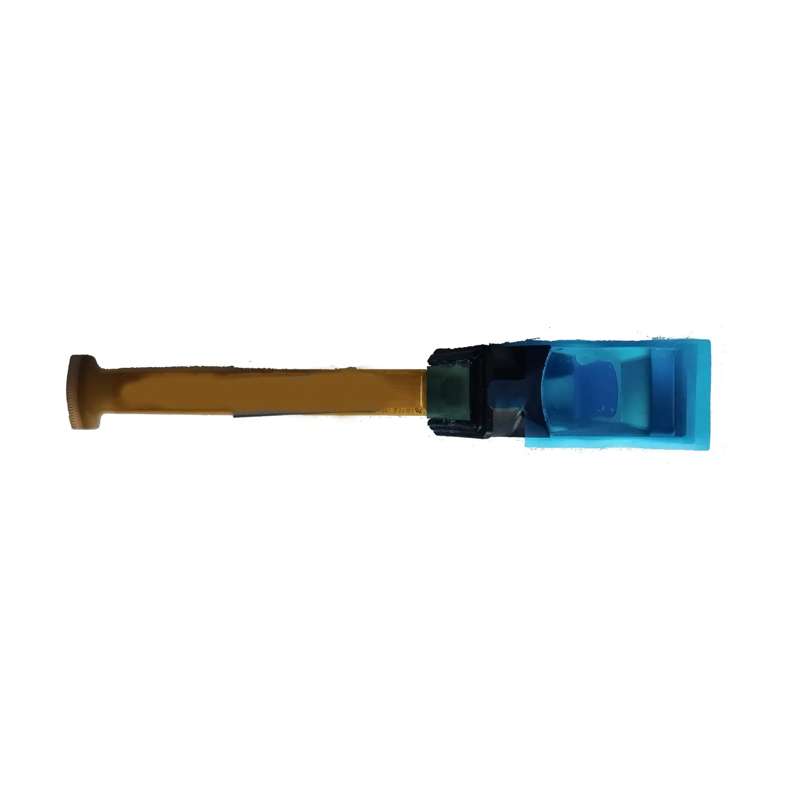
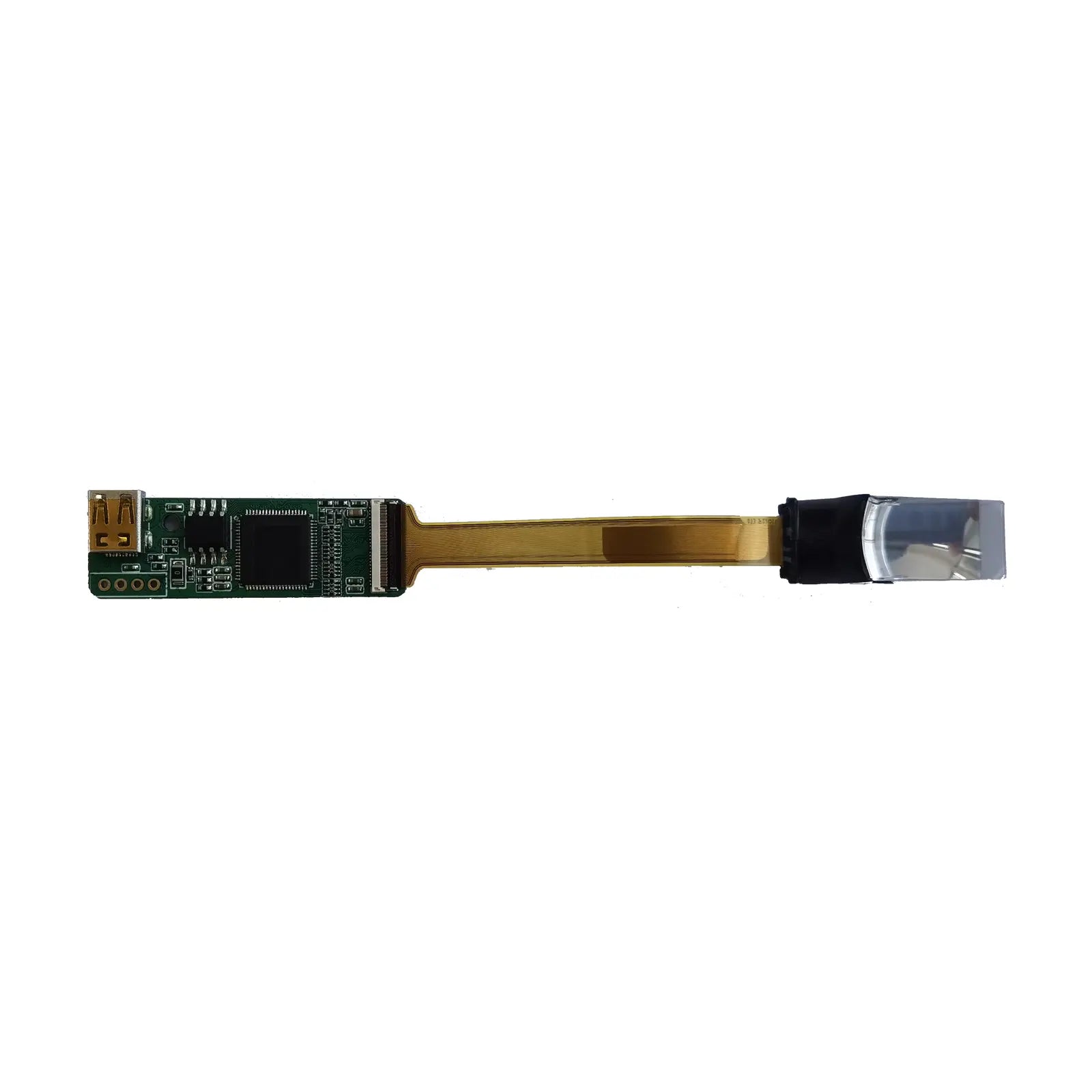
DM-ADTTR-024 MICRO OLED DISPLAY MODULE
0.23" Micro OLEDoS Display, 640(RGB) × 400, 2400 cd/m², 60Hz
0.23-inch active matrix color Micro OLED display module built on a single-crystal silicon transistor backplane. The module integrates the panel driver and logic driver, reducing external circuit complexity for compact optical engines, electronic viewfinders, wearable viewer products, portable instruments, medical visualization viewers, and enclosed near-eye display systems.
The native resolution is 640(RGB) × 400. The active format equals 256,000 full-color pixels and approximately 0.77 million RGB sub-pixel dots. With a 0.23-inch diagonal and 16:10 image ratio, the calculated pixel density is approximately 3,280 PPI. Final mechanical fit, active area tolerance, register values, and electrical limits should be verified against the official datasheet before tooling or mass production.
640 × 400
Native RGB resolution
2400 cd/m²
Maximum luminance
10,000:1
Contrast ratio
60Hz
Frame refresh rate
Calculated Engineering Values
Aspect Ratio
16:10, calculated from 640 × 400 active pixels.
Full-Color Pixels
256,000 full-color pixels.
RGB Sub-Pixel Dots
640 × 400 × 3 = 768,000 dots, approximately 0.77M dots.
Approximate Pixel Density
Approximately 3,280 PPI, calculated by diagonal pixel count divided by 0.23 inch.
Estimated Active Size
About 4.96 mm × 3.10 mm when calculated from the 0.23-inch diagonal and 16:10 ratio. Use the official mechanical drawing for production design.
Design Verification
Confirm active area, FPC tolerance, connector location, register values, power sequence, and optical alignment with the latest datasheet.
Optical, Electrical & Interface Specifications
|
Parameter |
Specification |
Engineering Note |
|---|---|---|
|
Display Technology |
Active Matrix Color OLED, Micro OLEDoS |
Single-crystal silicon transistor backplane |
|
Diagonal Size |
0.23 inch / 0.6 cm diagonal |
Designed for compact optical modules |
|
Resolution |
640(RGB) × 400 dots |
16:10 format, 256,000 full-color pixels |
|
Number of Dots |
0.77M RGB sub-pixel dots |
640 × 400 × 3 = 768,000 sub-pixel dots |
|
Calculated Pixel Density |
Approximately 3,280 PPI |
Calculated from 640 × 400 pixels and 0.23-inch diagonal |
|
Maximum Luminance |
2400 cd/m² |
Final eye-side brightness depends on optical transmission |
|
Contrast Ratio |
10,000:1 |
Useful for dark scenes and high dynamic image content |
|
Frame Rate |
60Hz |
Match controller timing and register initialization |
|
Input Interface |
Parallel RGB 24-bit, YCbCr 24-bit, YCbCr 16-bit |
Confirm host controller output format before PCB design |
|
Power Supply |
1.8V, 10V VCCP, EL cathode power supply |
Power-up sequence must follow datasheet limits |
|
Driver Integration |
Panel driver and logic driver integrated |
Reduces external driver component count |
|
Operating Temperature |
Refer to official datasheet |
Do not replace datasheet values with assumptions |
Architecture & Integration Details
Silicon Backplane OLED
The emissive OLED pixel array is formed on a single-crystal silicon transistor backplane. This architecture enables high pixel density in a 0.23-inch diagonal format and supports compact optical magnification paths.
Multiple Input Formats
Parallel RGB 24-bit, YCbCr 24-bit, and YCbCr 16-bit inputs are supported with register settings. Confirm color format, timing, and data mapping before firmware freeze.
Power Rail Planning
The module uses 1.8V, 10V VCCP, and EL cathode power supply. Check sequencing, ripple, inrush current, and absolute maximum ratings in the datasheet before PCB layout.
Scan Direction Selection
The display supports up/down and right/left scan direction selection. This helps match mirror, prism, lens, and board-orientation constraints in compact optical systems.
Optical Design Notes
Near-Eye Display Fit
A calculated pixel density near 3,280 PPI supports magnified viewing in compact optics. Final perceived sharpness depends on lens MTF, eye-box size, focus distance, and optical alignment tolerance.
Brightness Calculation
Panel-side maximum luminance is 2400 cd/m². System-side luminance should be calculated as panel luminance × optical path transmission × brightness setting. Measure after lens, prism, waveguide, or viewfinder optics.
Contrast & Black Level
OLED pixels emit light directly without a backlight layer. The specified 10,000:1 contrast ratio is useful for dark UI, camera preview, thermal image palettes, and high-contrast instrumentation graphics.
Design-In Checklist
Confirm Timing Before PCB Layout
Lock the RGB or YCbCr data format, pixel clock, sync polarity, blanking timing, reset sequence, and register initialization table before schematic release.
Validate Power Sequencing
Check 1.8V logic supply, 10V VCCP, EL cathode supply, enable timing, discharge path, and ripple limits. Use oscilloscope verification on first article boards.
Review Mechanical Drawing
Use the official drawing for display center, active area, FPC exit direction, connector location, keep-out zone, and optical axis alignment.
Request Evidence for Production
For mass production, request datasheet revision, sample test record, RoHS or REACH declaration if required, long-term supply status, packing method, and ESD handling instructions.
Application Fit & Verification Points
Electronic Viewfinders & Closed Near-Eye Viewers
Use case: compact EVF, inspection viewer, VR-style enclosed optics, and handheld optical viewing systems where ambient light is controlled.
Verify: lens magnification, focus distance, perceived brightness, color mapping, frame timing, and thermal rise inside the final enclosure.
Medical & Industrial Optical Instruments
Use case: compact medical viewer, endoscope display path, inspection device, microscope accessory, or portable visualization subsystem.
Verify: certification requirements, cleaning environment, optical alignment, reliability plan, color calibration, and device-level compliance.
AR Optical Evaluation Note
The 2400 cd/m² panel-side luminance should be evaluated carefully for see-through AR systems using waveguide or birdbath optics.
Because optical transmission loss can be significant, this module is better positioned for controlled-light or enclosed near-eye systems unless the final optical path and eye-side brightness are validated.
Oriented Technical
Documented Data
Resolution, dot count, luminance, contrast ratio, interface format, frame rate, driver integration, and power supply rails are listed for engineering review. Operating temperature and absolute maximum values should be taken from the official datasheet.
Engineering Review Before Design-In
Before final selection, review the datasheet revision, initialization code, signal timing chart, mechanical tolerance, connector drawing, optical test conditions, reliability conditions, and supply lifecycle status.
Procurement Verification
For OEM purchasing, confirm sample availability, bulk lead time, packaging method, ESD handling, lot traceability, warranty terms, change notification process, and long-term supply plan.
Mechanical Reference
Module Dimension View

Connector and Assembly Reference

Use these drawings for preliminary evaluation only. For production tooling, verify active area center, FPC tolerance, connector direction, mounting method, optical axis, and keep-out area with the latest official drawing package.
Download Datasheet & Confirm Optical Integration
Use the official datasheet to confirm mechanical drawings, electrical limits, timing details, register settings, power sequence, and optical alignment requirements before PCB layout or optical engine tooling.
For near-eye systems, calculate final eye-side brightness from panel luminance, optical path transmission, brightness setting, and target ambient-light conditions.
Download Official Datasheet