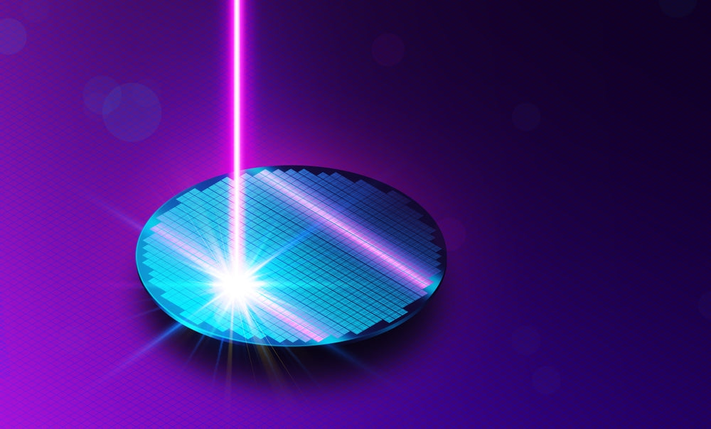
The photolithography process is a critical step in the manufacturing of array substrates for liquid crystal displays. It involves transferring patterns from a mask onto a photoresist layer using ultraviolet (UV) light. This process can utilize either positive or negative photoresist, where the pattern transfer mechanism differs based on the type of photoresist used:
• Positive Photoresist: The areas exposed to UV light become soluble, allowing the pattern from the opaque regions of the mask to be transferred to the photoresist.
• Negative Photoresist: The areas exposed to UV light become insoluble, transferring the pattern from the transparent regions of the mask to the photoresist.
In array engineering, the photoresist acts as a mask. The UV exposure creates a photoresist pattern that protects the underlying thin film during the etching process. After etching, the photoresist is removed, leaving the desired pattern on the thin film. This entire sequence of steps—film deposition, photoresist coating, exposure, development, etching, and photoresist stripping—constitutes the photolithography process.
Five-Step Photolithography Process
The formation of patterns on the array substrate typically employs a five-step photolithography process, especially in the back-channel etch (BCE) approach. Here’s a detailed look at each step:
1. Gate Metal Formation:
• Step 1: A metal layer is deposited on the glass substrate.
• First Photolithography Process: The gate metal pattern is created.
2. Active Island Formation:
• Step 2: A sequence of layers is deposited, including the gate insulator (g-SiN_x), the semiconductor layer (a-Si:H), and the ohmic contact layer (n^+ a-Si:H).
• Second Photolithography Process: The active island pattern is formed.
3. Source/Drain Formation:
• Step 3: Another metal layer is deposited.
• Third Photolithography Process: The source and drain patterns, along with the channel, are created.
4. Passivation Layer and Via Formation:
• Step 4: A passivation layer (PVX, typically SiN_x) is deposited.
• Fourth Photolithography Process: Vias (contact holes) are formed in the passivation layer.
5. Pixel Electrode Formation:
• Step 5: A transparent conductive layer (usually indium tin oxide, ITO) is deposited.
• Fifth Photolithography Process: The pixel electrode pattern and the via connection pattern are created.
Detailed Process Steps
Thin Film Deposition
The initial step in each photolithography cycle involves depositing thin films of various materials onto the substrate. These materials include metals for electrodes, insulators, semiconductors, and transparent conductors. The quality and uniformity of these films are crucial for the subsequent photolithography and etching processes.
Photoresist Coating
After deposition, a layer of photoresist is uniformly applied to the substrate. The thickness and uniformity of the photoresist layer must be carefully controlled to ensure accurate pattern transfer.
Exposure and Development
During exposure, UV light passes through the mask, transferring the desired pattern onto the photoresist. The exposure parameters, such as light intensity and exposure time, must be precisely controlled. After exposure, the substrate undergoes a development process, where the soluble regions of the photoresist are removed, revealing the pattern.
Etching
The exposed areas of the underlying thin films are etched away, either through wet or dry etching techniques. The etching process must be carefully controlled to achieve the desired pattern dimensions and ensure minimal damage to the underlying layers.
Photoresist Stripping
Once the etching is complete, the remaining photoresist is stripped away, leaving the patterned thin film on the substrate. This process must be thorough to ensure no residue remains that could affect subsequent processing steps.
Color Filter Photolithography
In the color filter fabrication process, the photoresist also serves as the pattern material for the color filter substrate. The same principles of exposure, development, and thermal treatment are applied to transfer the desired patterns from the mask to the color filter layers, achieving the necessary design specifications.
Read more

Liquid Crystal Displays (LCDs) employ various display modes, each with unique pixel structures and design intricacies. The most common modes include: • Twist Nematic (TN) Mode: Known for its fa...
Liquid crystal molecules exhibit electrical anisotropy, meaning their dielectric constant varies along different axes. When the dielectric constant along the long axis is greater than that along t...


Leave a comment
This site is protected by hCaptcha and the hCaptcha Privacy Policy and Terms of Service apply.